The stream processes can be described algorithmically.
3.1. Bit-Stream Algorithms
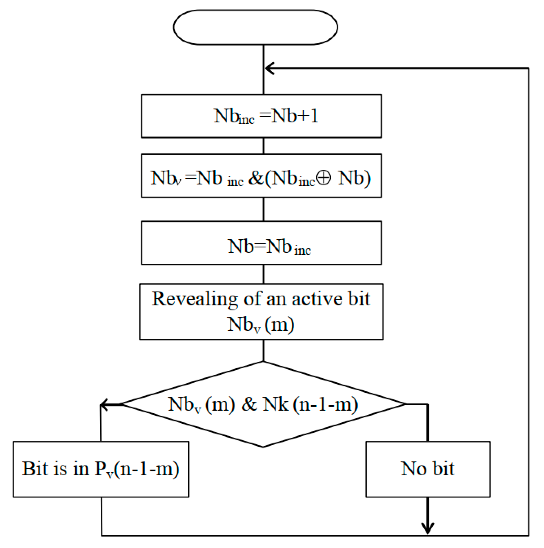
The conversion of the code into a pulse-frequency stream is based on the method of small increments. According to this method, the input code is represented as a stream of single bits occurring at fixed moments of time, ti. The number of pulses per process period is equal to the normalized value of the code.
Figure 2 shows the algorithm of pulse-frequency sweep.
When performing the sweep of the n-bit binary code , n bit streams are formed in parallel.
The algorithm works as follows: some base code n-bit binary code at each moment of time ti is incremented by 1, and code is formed.
The value of is compared with in order to find the position m (0 ≤ m ≤ n − 1), where code contains 1, and code contains 0. If such a combination is found, then a single bit is generated in the stream with the number n − 1 − m ().
The converted code is used as a mask of the current state of the streams . For masking, we use the following rule: the least significant bit 0 of the binary code masks the stream , formed on the basis of the most significant bit of codes , and the most significant (n − 1) bit codes masks the stream . The result of the masking makes it possible to determine the necessity of the bit generation to represent the code at the current time ti.
Table 1 shows an example of obtaining the bit streams
for n = 4.
When considering the sweeping of the code , if (binary equivalent: 0111), the streams will be selected. The zero value of the most significant bit of the code blocks the stream . The merging of bits of streams allows the formation of a stream in which the number of bit pulses per period is equal to the value of the sweeping code . If (binary equivalent: 1100), then and streams are selected. The sum of bits in and is equal . The streams , are blocked by zero values of bits number 0 and number 1 of the code.
The multiplication of PFM and PWM data is realized by passing bits of the PFM stream only at times when the PWM signal is active (equal to 1).
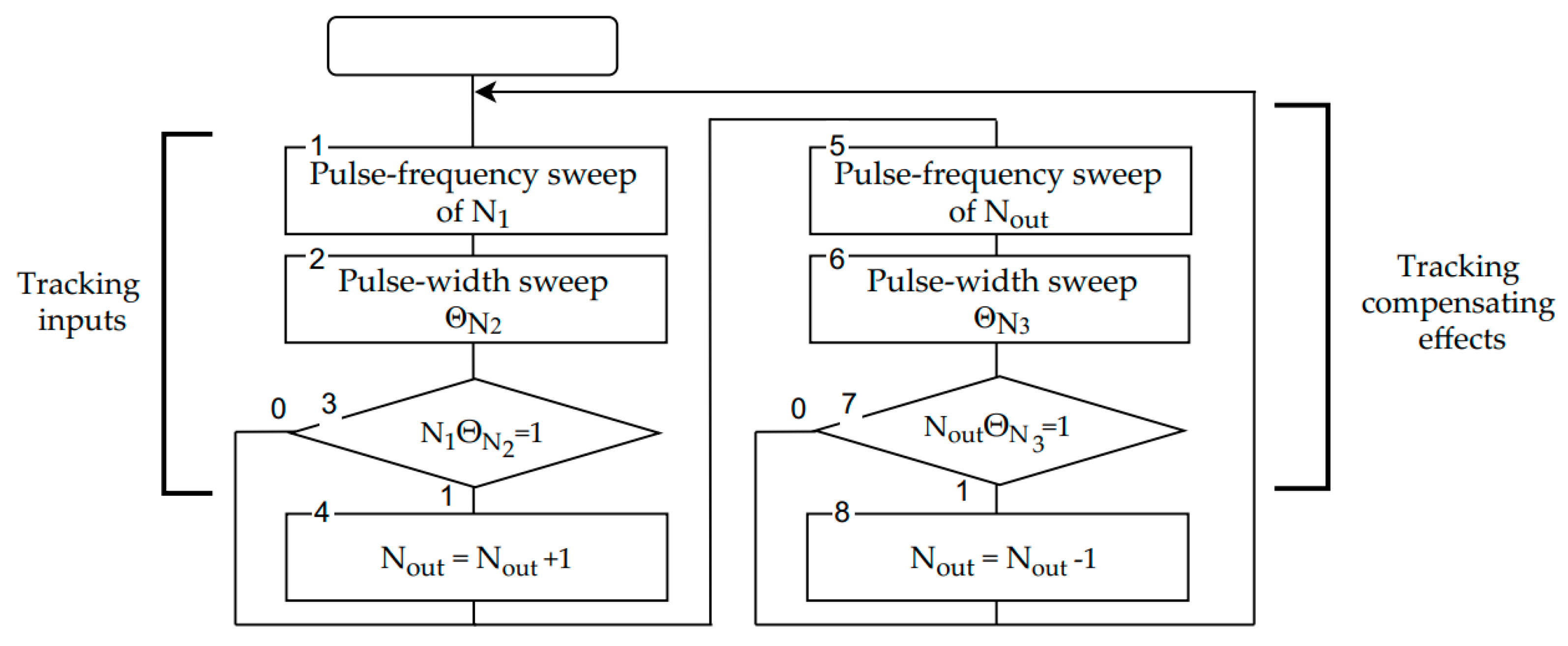
We used the multiplication-division operation algorithm shown in
Figure 3 to implement function (1). One of the input numerator codes, e.g.,
, is converted into a bit stream, and the code
is converted into a PWM signal
. As a result of bit-stream multiplication, the value
is formed.
The result calculation starts when the bit corresponding to the code value appears, i.e., the output code is incremented when (blocks 3, 4). If after the pulse frequency sweep of the code the bit is not formed, the output code does not change.
To form the compensatory actions, the denominator code is converted into a PWM signal . The code is converted into a bit stream, and the result of multiplying in the compensation branch of the algorithm is the value of . When = 1 (blocks 7, 8), it is necessary to form a compensating bit. When the compensating bit appears, the compensation mechanism starts working, and the code is decreased by one. If = 0, then the bit in the compensatory stream is not formed, and the output code does not change. Operations 1–3 and 5–7 can be executed in parallel.
At the initial stage of the algorithm operation, the number of compensating actions is small, but as the output code increases, the stream in the compensating loop becomes more intense. This continues until the process reaches equilibrium, characterized by the equality of the intensities of the streams causing the increments and decrements. If equilibrium is reached, the code is the result of calculations. If the streams change randomly during the computation, the equilibrium is disturbed and automatically compensated, and the result is restored. Any changes in the input signal lead to the transition of the computational process to a new equilibrium state.
The period T of the algorithm operation is determined by the selected bit width of codes and is T = 2n ti, where ti is the time interval determined frequency of the process quantization. The description of the computational process is based on the time interval ti, chosen as the unit time, and then in relative units T = 2n. The number of time samples ti per period T is denoted as .
The input and output codes are scaled by the maximum value in the used bit grid. A scaling factor equal to one is taken, so that the maximum values of and coincide with the maximum value of the period T in relative time units.
The number of bits in the stream generated from the input signals during the period T is determined as
The number of time segments t
i per period can be any number. By taking
, this simplifies the mathematical description of the process but does not change its essence. Formula (2) can be written as follows:
In a similar way, we can determine the number of bits generated in the compensating branch during the period T:
The sampling frequency of the process when forming compensation streams is the same as when tracking input codes,
. Formula (3) can be written as follows:
After completion of the first period of signals
and
, i.e., after 2
n cycles of the work of multiplication-division algorithm, the output code is defined as follows:
where
is some initial value of the output code.
At the end of the algorithm second period, the following code is generated:
The result after the i-th period is defined as
The second term of this expression is a geometric progression with base q = 1 −
It can be replaced by the amount
Thus, the function describing the result of the algorithm at the end of period t is defined by the following expression:
As for the value of
, when it lies in the range of 0 <
< 1, we can use the following equations:
Thus, in the equilibrium state, the output code
is determined by the following dependence:
The time to reach the equilibrium state is determined by the number periods, T.
If the process quantization frequency is high, we can treat the sequence of output codes as a continuous function. Therefore, the dynamics of the transient process can be determined using the following equation:
The equation describes the process of transition to the tracking mode as the process of accumulating the difference of incrementing and decrementing streams during each period T. If the values
,
,
do not change during the transition process, the equation for the variable t can be solved as follows. Differentiating the right and left parts of the equation, we have
We integrate the expression and obtain
As a result of the transformation of this expression, we can get
The dependence of the transient duration is logarithmic, and its parameters are determined by the combination of input data and the initial state of the process.
3.2. Algorithm Implementation
We use VerilogHDL to implement and verify the considered algorithms. The VerilogHDL behavioral descriptions can be used to synthesize hardware modules.
The input signals of the pulse frequency sweep module are the reference frequency signal clk and the input code Nk. The pulse stream Fout is generated at the output of the synthesized module.
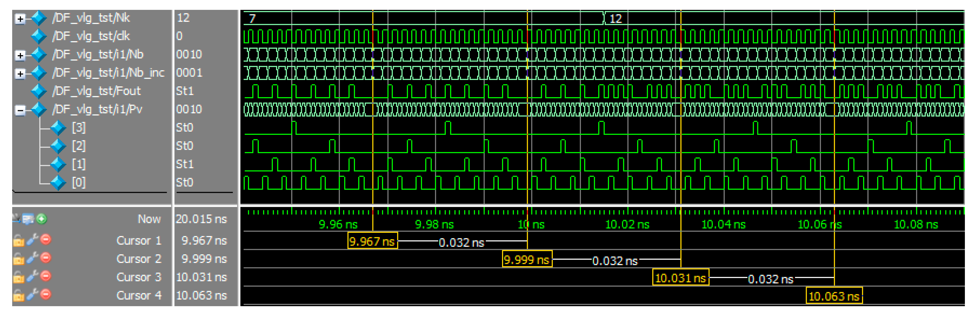
Figure 4 shows the result of the Verilog module simulation with the ModelSim.
To test the module, we used a TestBench. It is a non-synthesizable fragment of the VerilogHDL program that continuously generates the clock signal clk with frequency fclk as well as the changing input code Nk. The function $urandom_range is used to generate the input code in a bit grid i; the frequency of code Nk changing during the test is fclk/(3 × 2i).
The bit width of the processed codes Nk is 4, so the pulse-frequency sweeping algorithm generates 4 pulse streams –. The lines DF_vlg_tst/i1/Pv[3...0] of the diagram show the generation of these streams. The total number of pulses in these streams during one period corresponds to the maximum possible value of the code represented in the 4-digit grid, and this value is equal to 15.
Three periods of algorithm operation are highlighted in
Figure 4. The first period (time marks 9.967–9.999) shows the code Nk = 7 conversion. The number of pulses generated during the period of algorithm is 7 (line DF_vlg_tst/Fout). The second period is transitional. In this period the input code Nk is changed, so part of the period the output pulse stream is formed on the basis of the code Nk = 7, and then for Nk = 12. The third period (time marks 10.031–10.063) shows the code Nk = 12 conversion. The number of pulses generated per the period of the algorithm at the DF_vlg_tst/Fout output is 12.
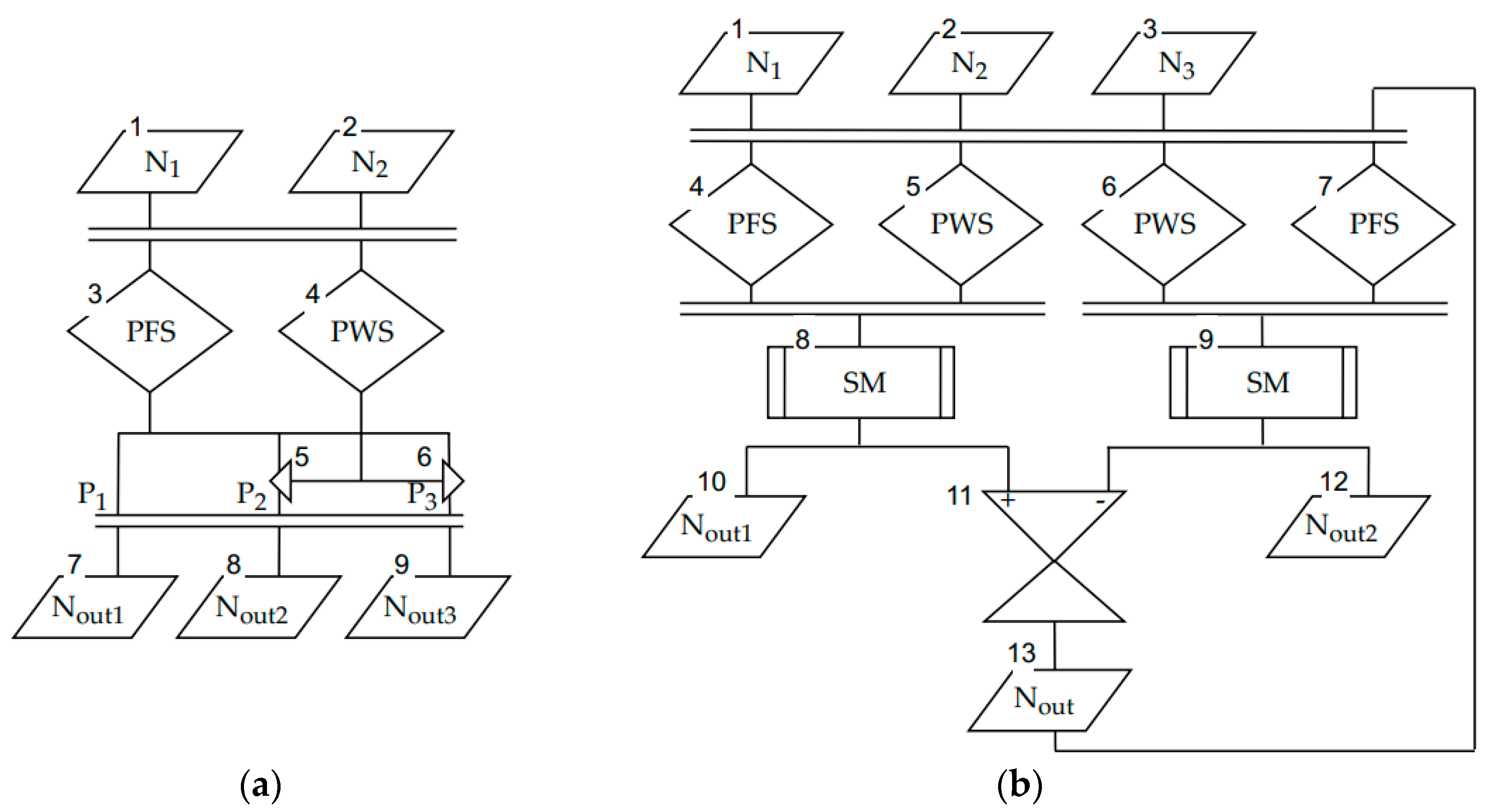
The streaming multiplication-division module calculates the function using formula (1). We simulate it with the use a 10-bit implementation.
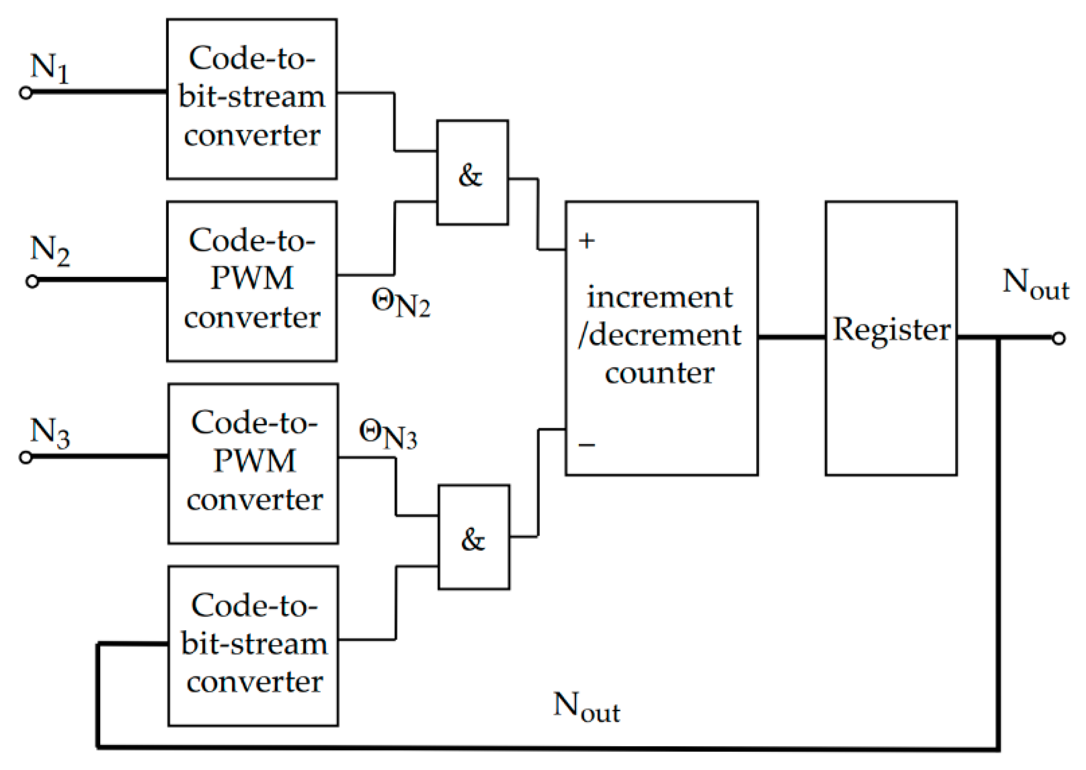
A generalized block diagram of the module is shown in
Figure 5.
The scheme contains the following sub-modules:
two code-to-bit-stream converters performing the conversion of codes
and
into a bit stream using the
Figure 2 algorithm and implementing the operations of blocks 1 and 5 of the algorithm shown in
Figure 3;
two code-to-PWM converters performing the conversion of
and
codes into a stream of PWM signals; they implement the operations of blocks 2 and 6 of the
Figure 3 algorithm and can be implemented by known methods, for example, using counters;
two «&» elements performing multiplication of bit stream by PWM signal (blocks 3 and 7 of the
Figure 3 algorithm);
increment/decrement counter, which counts the pulses generated in the positive and negative branches of the unit (blocks 4 and 8 of the
Figure 3 algorithm).
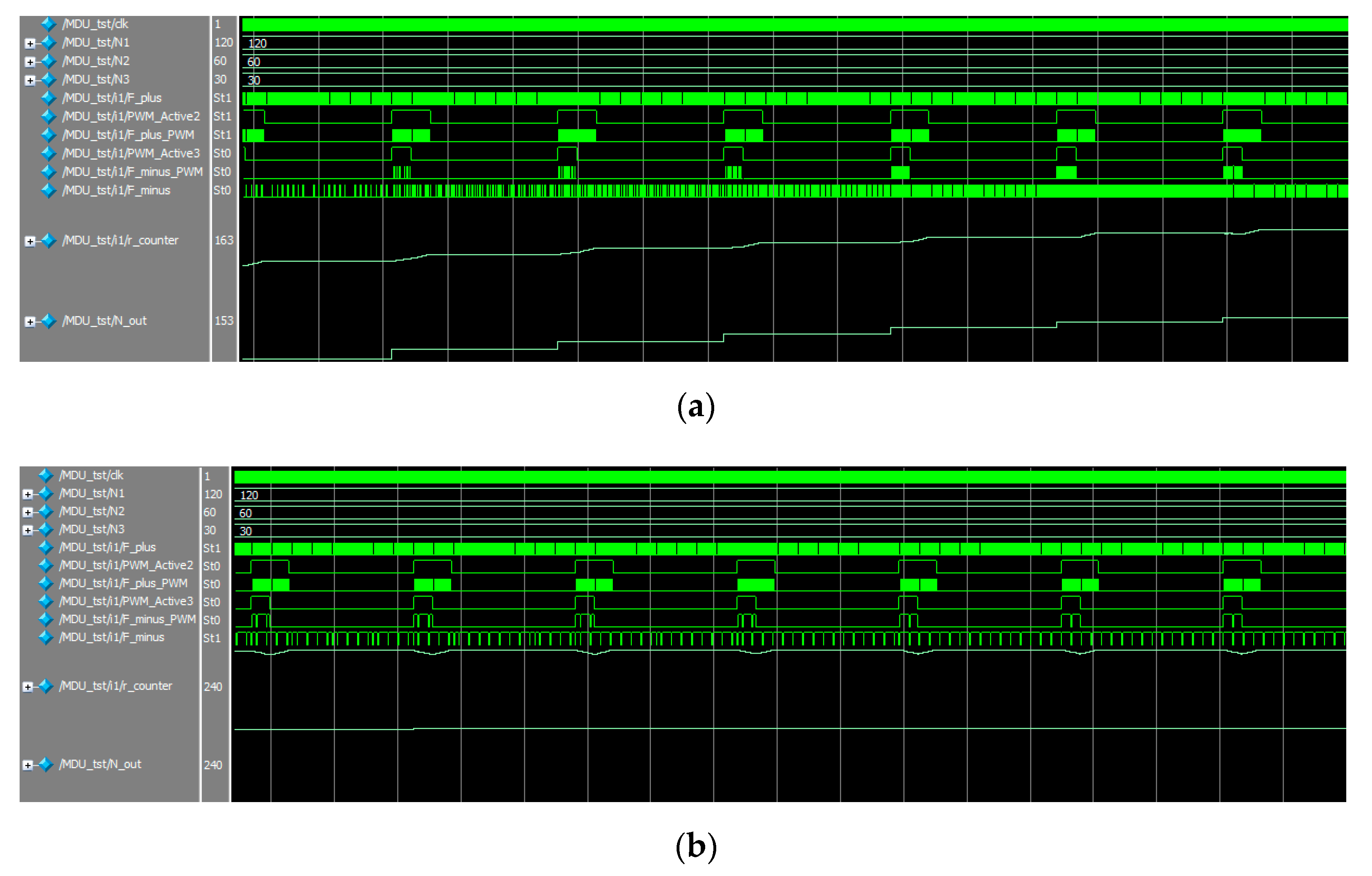
Figure 6 shows the processes in the multiplication-division module.
To test the streaming multiplication-division module, we used TestBench, in which the clock signal clk was formed continuously and the input codes N1, N2 and N3 were formed using the function $urandom_range. The frequency of change of input codes was chosen so that on the time diagram we could observe the transient process when the device tends to an equilibrium state, as well as the process of holding the stable state.
The input code N
1 is converted into a pulse stream (line MDU_tst/i1/F_plus). The codes N
2 and N
3 are converted into PWM signal streams (line MDU_tst/i1/PWM_Active2 and MDU_tst/i1/PWM_Active3).
Figure 6a shows the transient where the resulting signal (MDU_tst/i1/r_count) increases on each cycle, coming closer to the result. The corresponding pulse stream becomes more intense on each cycle (MDU_tst/i1/F_minus). At the digital output (MDU_tst/i1/N_out), the data is fixed at the end of each period; this allows for a stable output code value during the period.
Figure 6b shows the process of tracking the result in the equilibrium state. The resultant signal (MDU_tst/i1/r_count) changes during each cycle, but by the end of the period it retains the value recorded at the end of the previous cycle. The corresponding pulse stream (MDU_tst/i1/F_minus) does not change. The digital output (MDU_tst/i1/N_out) stores the result in digital form. For given values N
1 = 120, N
2 = 60, and N
3 = 30, the result Nout = 240.
3.3. Application of the Developed Modules
The designed behavioral HDL modules are used in the design of the temperature regulator built into the human blood cholinesterase activity analyzer. This device provides analytical procedures with biological liquids. According to the rules of analysis, it is necessary to keep the temperature of the analytical solutions between 34 and 39 °C, since cholinesterase activity depends on temperature [
18].
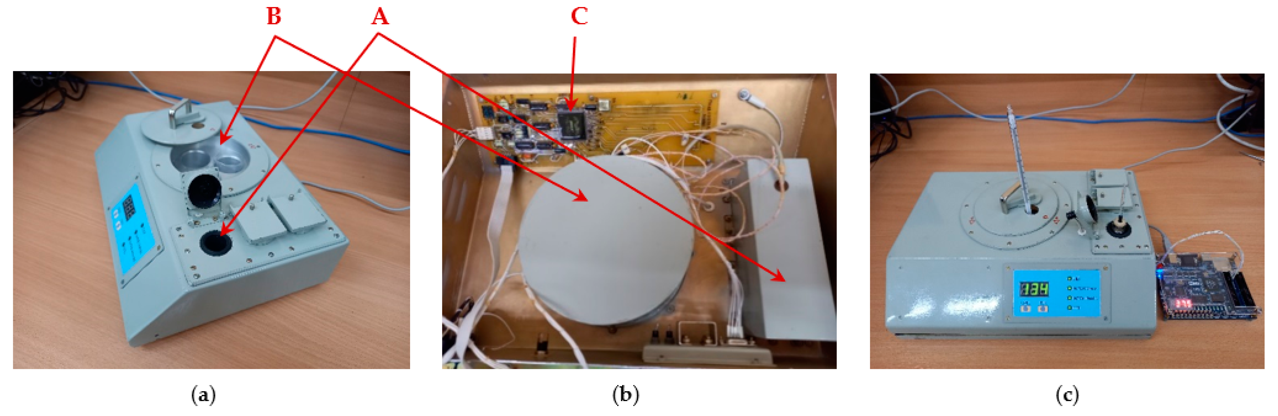
Figure 7 shows the cholinesterase activity analyzer. Thermal control is performed independently in two elements of the device: the measuring cuvette (A) and the reagent platform (B).
Measurement of cholinesterase activity is performed by measuring the time that the optical density of analytical solution changes by 10% from the initial value. The reservoir with analyte is placed in the measuring cuvette (A); the temperature of measuring cuvette is maintained within the specified range. The Analog Devices TMP03 sensor used for temperature control is inserted into the hole on the back side of the measuring cuvette using the thermally conductive paste.
The aluminum platform (B) is used to preheat the reagent containers to the specified temperature. To control the platform temperature, a second AD TMP03 sensor is installed using a thermally conductive paste in the hole on the back of the platform. Both sensors generate PWM output signals continuously.
The analyzer does not have a processing core, and its elements and modules operate under control of a digital finite state machine implemented on the CPLD chip (C). CPLD do not have special hardware elements for arithmetic calculations, but the temperature measurement requires arithmetic conversions according to the sensor characteristic:
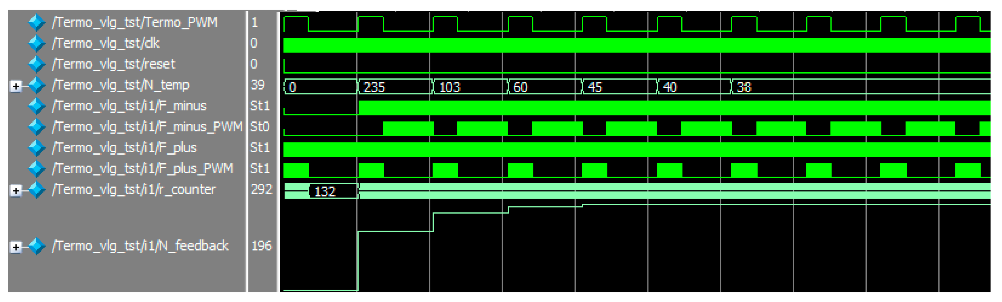
To calculate the temperature according to Equation (4), we used designed algorithm of multiplication-division operation (
Figure 3). In this case, the algorithm is not fully implemented; blocks 2 and 6 are not executed since the sensor signals are presented in the form of PWM, and operations to change the data format (pulse-width sweep, PWS) are not required. PWM signals come to processing immediately. The subtraction operation is also performed in stream form by decrementing constant 235 at the moment when the multiplication-division unit generates the next pulse of the output stream.
Figure 8 shows the result of the simulation of the processes occurring during temperature measurement.
We tested the algorithm operation during the experiments by means of an analyzer. To indicate the temperature, we used an external board with indicators, since the alphanumeric indicator of the analyzer is intended to display the results of the analysis of cholinesterase activity. The modules based on the behavioral description of the temperature meter were implemented into the CPLD (MAX3512), and the indicator of the external board showed the measurement results. At the same time, we monitored the temperature of the measuring cuvette and platform by means of mercury thermometers;
Figure 7c shows this process.
Rounding of the measurement results was performed with an accuracy of 0.5 °C, as the used sensor TMP03 for measurements in the range of 0–50 °C has such accuracy, and we conducted tests in this range. Mercury thermometers allow measurements with an accuracy of −0.1 °C. During the tests, the readings of the thermometers and the indicator of the device coincided.
The solution of this problem by the traditional method requires the use of calculators such as counters to determine the code values of the duration of PWM signals, multiplier, divider, and subtractor. These elements are available in the Quartus II library of parameterized modules. However, when selecting a chip of the CPLD class as a device, the compilation of the project finishes with error messages. To compare the traditional and bitstream approaches, we compiled a HDL description with FPGA selecting. The library elements were configured in a combinational way, and registers were not used. The results of the bit-parallel and bit-stream methods comparison are shown in
Table 2.
A hardware cost analysis shows the cost-effectiveness of the bit-stream implementation.
The frequency characteristics were analyzed using Time Quest Timing Analyzer. The maximum frequency fmax for the bit-parallel method was 35.94 MHz. For the bit-stream method, the maximum frequency was 111.73 MHz, but the processing period was related to the bit rate, and for the 10-bit device version the frequency was defined as fmax/210, or 109 kHz.
The conversion accuracy is determined by the bit rate of the device and can be corrected for additional bits if necessary.


