Article

Responsivity and Noise Equivalent Power of a Single Cold-Electron Bolometer

by
Ian Jasper Agulo
1,2,* and
Leonid Kuzmin
1,3
1
Department of Microtechnology and Nanoscience, Chalmers University of Technology, 412 96 Gothenburg, Sweden
2
Department of Physical Sciences, College of Science, University of the Philippines Baguio, Baguio City 2600, Philippines
3
Laboratory of Superconducting Nanoelectronics, Nizhny Novgorod State Technical University, 603950 Nizhny Novgorod, Russia
*
Author to whom correspondence should be addressed.
Appl. Sci. 2021, 11(10), 4608; https://doi.org/10.3390/app11104608
Submission received: 16 March 2021 / Revised: 22 April 2021 / Accepted: 28 April 2021 / Published: 18 May 2021
(This article belongs to the Special Issue Design and Application of Cold-Electron Bolometers)

Abstract

:
We have developed a single-pixel capacitively coupled Cold-Electron Bolometer (CEB) and characterized it in the current-biased regime. The most attractive feature of the CEB is effective electron self-cooling of the absorber, which leads to a lower bolometer noise and higher dynamic range. The bolometer responsivity was measured by determining the voltage response to an applied power through the absorber from a heating current, modulated at frequencies from 35 Hz to 2 kHz. The optimum responsivity of 1.5 × 10¹⁰ V/W was measured at a modulation frequency of 35 Hz. The noise equivalent power (NEP) was subsequently obtained from the estimated bolometer noise voltage with respect to the measured bolometer responsivity. The NEP of better 2 × 10⁻¹⁸ W/Hz1/2 was obtained for modulation frequencies greater than 100 Hz. The background power and the bolometer time constant were also estimated from the experimental results. The photon-noise-limited operation of CEB will dominate for a signal power of 10 fW and higher at frequency 80 GHz and higher.

1. Introduction

Great interest in the development of bolometers for radioastronomy applications has grown owing to the discoveries in the study of the cosmic microwave background (CMB) [1,2]. The primary purpose is to measure the remnant primordial B-mode polarization after the inflation stage of the universe’s evolution [3,4]. The proximate goal is to develop a single-pixel detector with a noise equivalent power (NEP) less than the photon noise over the 40–1000 μm wavelength for a wide range of optical power loads. The most widespread bolometers are the transition edge sensor (TES) [5] and the kinetic inductance detector (KID) [6]. The capacitively coupled Cold-Electron Bolometer (CEB) [7,8] is a very attractive option suited for this purpose, since it shows high immunity against cosmic rays [9] due to the extremely small absorber volume and strong decoupling of the electron subsystem from the phonon subsystem. Besides that, the CEB demonstrates effective electron self-cooling of absorber [10] that gives opportunity to achieve the photon-noise-limited operation at 300 mK without dilution refrigerator. Arrays of CEBs were tested already for relatively high optical power load as integrating bolometer [11,12,13,14]. CEB was also proposed as a single-photon counter [15]. The main problem of CEB is matching with SQUID readout due to relatively high resistance to create array of bolometers with multiplexing. The visible way is to create a parallel array of CEBs for decreasing total resistance [16]. In this paper, we report on the responsivity and electrical noise qualifications of the single-pixel CEB for a small optical power load.
The uniqueness of the CEB stems from the fact that it uses the heat energy absorbed to cool down the absorbing material, contrary to other detectors where the heat energy brings the device to saturation. The absorbed heat energy by the absorber is estimated as the increase in the electron temperature. The CEB concept is based on removing heat from the absorber (Figure 1) [8]. The absorber heat removal, which acts as a negative electrothermal feedback for the incoming signal, is achieved by two methods. The first is through the removal of heat by the SIN tunnel junctions and the dissipation of the removed heat to the superconducting electrodes. The second method of electron cooling is accomplished by adjusting the superconducting electrodes’ geometry to provide more volume for the diffusion of the tunneled quasiparticles and by connecting normal metal traps to the superconducting electrodes. The normal metal traps greatly enhance the electron cooling. We previously demonstrated an almost 200 mK decrease in electron temperature with the use of these traps [10,17]. These modifications considerably improve the noise properties and sensitivity of the device.
The CEB performance is best described through the following parameters: the responsivity, the sensitivity or noise equivalent power, and the time constant. In the current-biased mode, the responsivity, SV, is obtained by determining the voltage response, δ V ω , to the incident radiative power, δ P ω [18].
S V ω , I = δ V ω δ P ω
The noise equivalent power (NEP) or the sensitivity is the total of all the noise sources referred to the input of the bolometer with respect to the square root of the bandwidth. The total NEP is composed of three components given by [18]
N E P t o t a l 2 = δ V ω 2 a m p S V 2 0 , I + 10 k B Σ v T e 6 + T p h 6 + N E P S I N 2
The first expression on the right-hand side is the amplifier NEP, which is defined as the amplifier noise voltage, δ V ω a m p , over the square of the voltage response to the incident radiative power of the bolometer, S V 0 , I . The second term is the NEP associated with electron–phonon interactions, where Σ is a coupling constant, v is the absorber volume, and T e and T p h are the electron and phonon temperatures, respectively. The third term is the NEP associated with the SIN tunnel junction and is attributed to the shot noise, heat dissipation through the tunnel junctions, and the correlation between these two processes. Theoretically, the CEB should achieve a NEP of 10−19 W/Hz1/2 [6,18]. The detection of a 1–30 pW signal by a CEB with an NEP of photon noise greater than the CEB NEP has been shown very recently for arrays of CEBs [11,12]. This paper demonstrates a voltage response to power of 109 V/W and a NEP of better than 10−18 W/Hz1/2 at 100 mK in the current-bias mode for a single-pixel CEB.

2. Materials and Methods

To fabricate the CEB with a small volume, a two-layer resist technology was used to implement the two-angle evaporation method using electron beam lithography. Gold was used as the primary electrode material, with chromium deposited before gold to improve the adhesion of gold to the SiO2 substrate. Palladium was also deposited on top of the gold layer as a buffer between gold and aluminum, preventing the formation of a gold and aluminum alloy to increase the contact resistance. The standard two-layer resist technology, using a 0.2-μm-thick PMMA layer on top of a 0.8-μm-thick Copolymer, was used to create the device’s masks. The device consists of a superconducting electrode, the small-volume normal metal absorber, and the superconductor-insulator-normal metal (SIN) tunnel junction. The two-layer technique makes it possible to create all three device components in just one vacuum cycle.
To fabricate the bolometer device, an aluminum electrode was used as the superconducting electrode, and chromium was used as the normal metal absorber. Chromium adheres better to the substrate and provides good impedance matching between the absorber and the antennae. To implement the two-angle evaporation method, the superconducting aluminum was first thermally evaporated at an angle, followed by the oxidation of the aluminum film, and then finally with the deposition at an angle of 0° of the normal metal chromium and copper. It was found that the optimal angle of evaporation for aluminum was 55° with respect to the normal of the film surface. The aluminum thickness was about 60 nm. Aluminum was oxidized for 2 min at a pressure of 5 × 10⁻² mbar. The normal metal absorber was composed of 30 nm-thick chromium film and 30 nm-thick copper film. After the vacuum deposition process, the e-beam resist was removed by lift-off in acetone.
To simulate the theoretical prediction [15] and compare it with the experimental results, we used the heat balance equation given by
P e p h + P R S + P 0 = P c o o l
where P e p h = Σ v T e 5 T p h 5 is the heating due to the electron-phonon coupling, P R S = 2 V 2 / R S is the Joule heating from resistance in the subgap region, R S , P 0 is the absorbed heating power, and P c o o l is the cooling power of the SIN tunnel junctions. The parameter, earlier defined in Equation (2) as a coupling parameter, has a value of Σ = 1.3   n W   K 5 m m 3 obtained from fitting against the measured responsivity and sensitivity. The volume of the absorber was with a resistance of 63 Ω.

3. Results

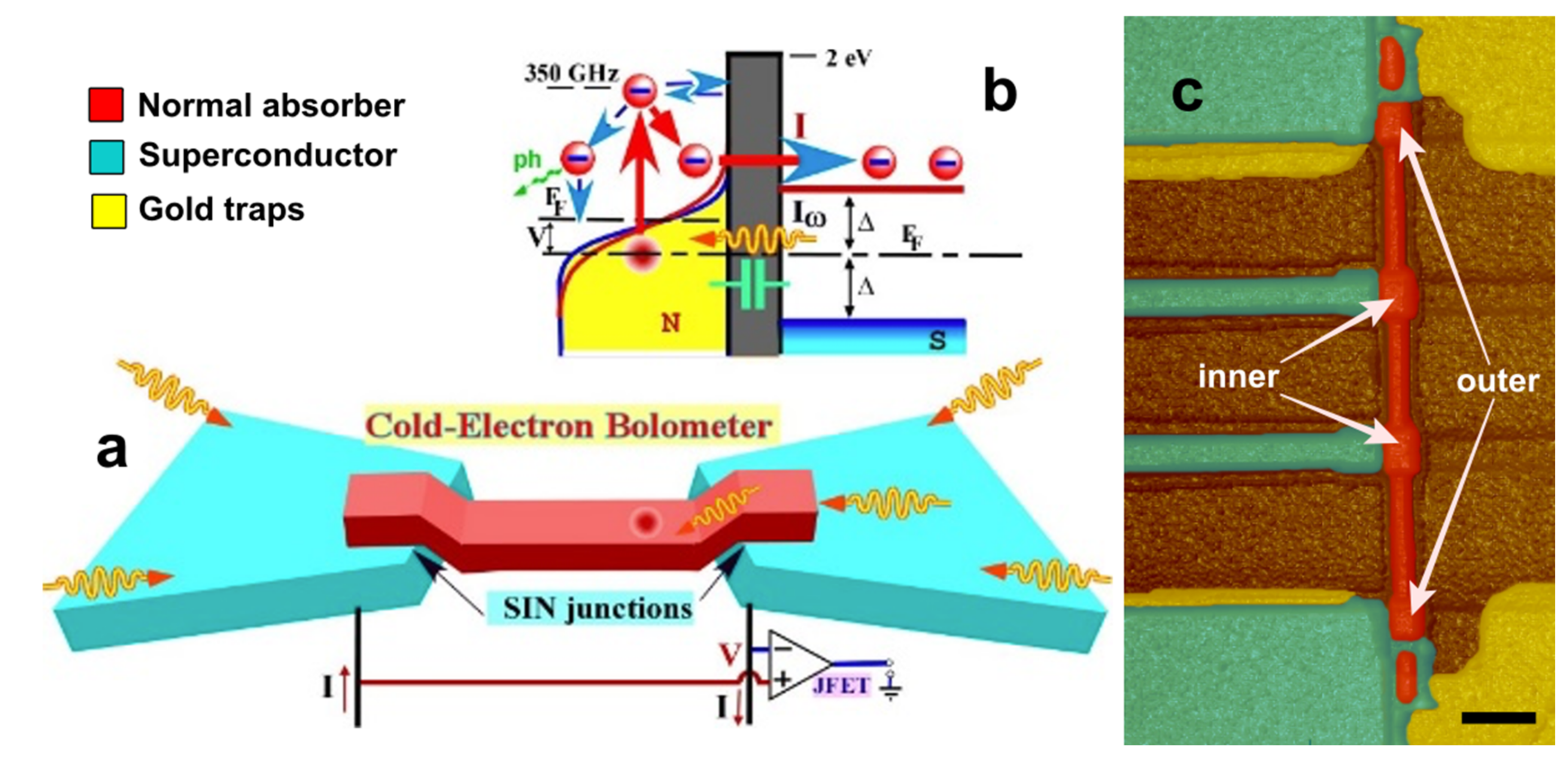
3.1. The Single CEB Device
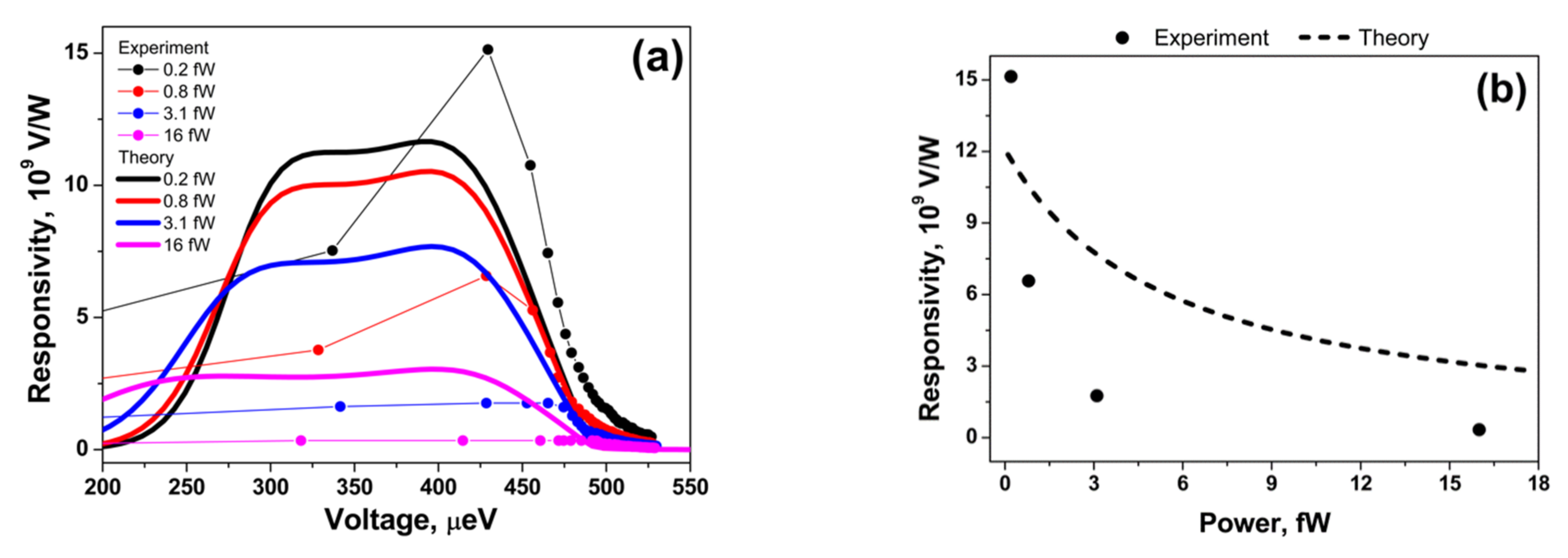
The fabricated CEB device is composed of an absorber with a very small volume of 0.11 μm3 and four superconductor-insulator-normal metal (SIN) tunnel junctions (Figure 1) [10,17]. The measured resistance of the absorber was 63 Ω. The two outer SIN junctions each have an area of 0.45 μm2, with a normal resistance of 4.3 kΩ and a subgap resistance of 8.4 MΩ. The outer SIN junctions serve primarily as electron coolers of the absorber, but also serve as a coupling capacitor of the absorber to the antennae and as thermal isolation. These three design improvements lead to the enhancement of the responsivity and the sensitivity of the bolometer. The two inner SIN junctions each have an area of 0.06 μm2, with a normal resistance of 14.5 kΩ and a subgap resistance of 21.2 MΩ. The inner SIN junctions act as thermometers measuring the electron temperature of the absorber. The SIN thermometer was calibrated to estimate the electron temperature from the measured junction voltage. The optimal bias current was obtained during calibration to be 20 pA, with an estimated background power load of 22 fW. These junctions should have minimal influence on the device since they were designed to have a smaller area than the outer tunnel junctions.
The incident power is applied to the outer tunnel junctions increasing the electron temperature of the absorber. These junctions adjacent to the gold electrodes, also remove the hot electrons from the absorber to the electrodes serving as traps. This design allows for better dissipation of hot electrons, reducing backflow to the absorber. The two inner tunnel junctions measure the electron temperature changes and are observed as a voltage change across the two inner tunnel junctions measured by a read-out amplifier. The voltage of the superconducting gap was estimated to be 568 μeV from fitting the measured I-V curve of the inner tunnel junctions with the theory.

3.2. Responsivity

The sample was placed in an Oxford Instrument’s TLE200 dilution refrigerator and was measured in the current-bias regime. The asymptotic junction resistances and the zero-bias and subgap resistances, were estimated with a symmetric voltage source with series bias resistances. The bias resistors, which also provide some degree of protection from external interference, range from 200 kΩ to 20 GΩ.
The responsivity, SV, is measured in this manner. A modulated signal, generated by internal oscillator of a lock-in amplifier, was biased with a resistor to produce the heating current, which was applied across the outer SIN tunnel junctions. This generates a voltage response across the inner tunnel junctions, measured with the SR830 lock-in amplifier. The dependence of the response across the inner junctions to the bias current was then measured, and then divided by the heating power. The heating power was estimated from the IV characteristics of the outer tunnel junctions. The bias current was converted to bias voltage using the IV characteristics of the response junctions. Figure 2 shows the dependence of the responsivity on the bias voltage for different heating powers of 0.2, 0.8, 3.1 and 16 fW at 35 Hz modulation. For comparison, the theoretical responsivity is also presented in Figure 2. The dependence of the maximum response on varying heating powers plotted against the theoretical responsivity, is shown in Figure 2b. The responsivity has a maximum value of 1.5 × 10¹⁰ V/W and decreases with increasing power at a modulation frequency of 35 Hz. The theoretical responsivity, shown as the dashed line in Figure 2b, has a similar trend to the experimental result.

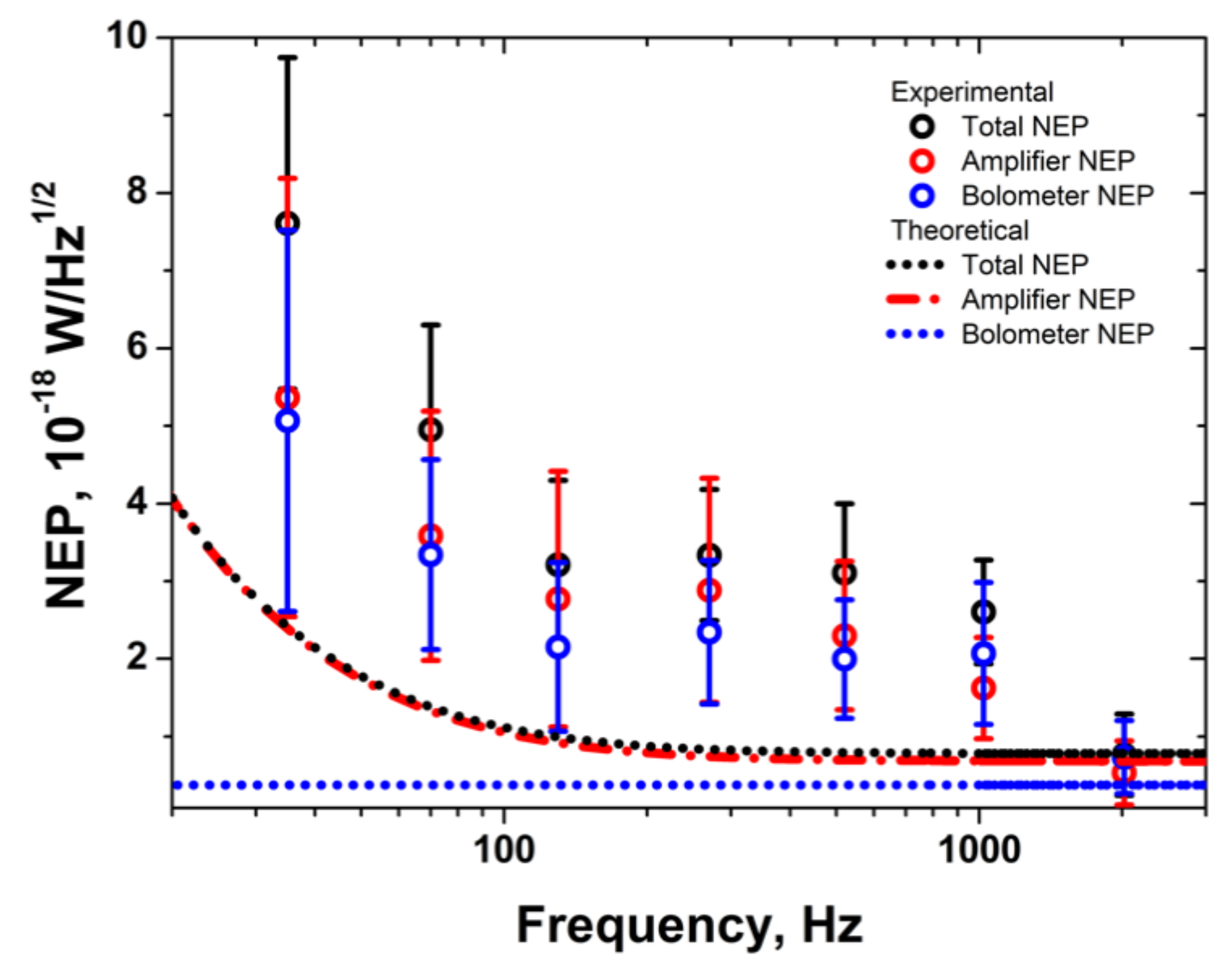
3.3. Noise Eqiuvalent Power

In this work, we present our measurements of the total NEP, the bolometer NEP and the amplifier NEP. The amplifier NEP is determined by dividing the measured voltage noise of the amplifier and the responsivity. The total NEP is obtained by measuring the voltage noise at the output of the preamplifier, which was then divided by the measured responsivity of the device. The bolometer NEP was then estimated from Equation (2), by subtracting the amplifier NEP from the total NEP. The total NEP, bolometer NEP and NEP of the amplifier from 35 Hz to 2 kHz is shown in Figure 3. The theoretical predictions for the total NEP, bolometer NEP, and NEP due to the amplifier are shown as dashed lines. At low frequencies, we include the 1/f noise due to the amplifier in our theoretical fit which agrees quite well with the experimental results at lower frequencies. As seen in Figure 3, the total NEP for all modulation frequencies is in the order of 10−18 W/Hz1/2. The maximum measured bolometer NEP is 5 × 10⁻¹⁸ W/Hz1/2 at 35 Hz, while the minimum measured bolometer NEP is 10−18 W/Hz1/ at 2 kHz. Photon noise at the level of 10−18 W/Hz1/2 is for a signal of 10 fW at a frequency of 80 GHz. That means that for the power and frequency of the signal higher than these values, photon noise will dominate over the noise of CEB.

3.4. Time Constant

The bolometer time constant of 6.3 μs was obtained by using the equation given by [15]
τ = γ T e v P t o t a l / T
where γ = 9.77 J/μm3K2 for copper, the volume, v , is the measured volume of the absorber of 0.11 μm3, and P t o t a l / T is the total thermal conductance.

4. Discussion

We designed a single pixel cold-electron bolometer with a maximum voltage responsivity 1.5 × 10¹⁰–1 × 10⁹ V/W from an absorbed power of 0.2–16 fW and a bolometer NEP of about 7.3 × 10⁻¹⁹–5.1 × 10⁻¹⁸ W Hz−1/2. The photon noise of the signal will dominate over the noise of CEB for a signal power of 10 fW and higher at frequency 80 GHz and higher. In a recent paper [11], in which Kuzmin et al. fabricated and measured the NEP of 192 CEBs, extrapolation to a single CEB gave a bolometer NEP of about 3 × 10⁻¹⁸ W Hz−1/2 at 300 mK, which is quite consistent with our experimental results.
The obtained results agree reasonably well with the theoretical predictions. The CEB noise is limited by the noise due to a room temperature amplifier. A cold amplifier or an amplifier with lower voltage noise would reduce its thermal noise. In this work, we used an OPA111 amplifier with a voltage noise of 8 nV/Hz−1/2. The AD743 or AD745 would be more suitable with a lower voltage noise and a lower impedance. Another method would be to improve the NEP by matching the dynamic resistance of CEB with the equivalent noise impedance of an amplifier. At the optimum bias current, the resistance of the CEB is in the order of 60 kΩ and the source impedance for a typical amplifier (e.g., OPA111) would be around 15 MΩ. Thus, an array of CEBs would have good impedance matching with these low noise amplifiers [8,11]. Additionally, analyses by Golubev and Kuzmin of the CEB made [15] indicate that in order to achieve enhanced responsivity and NEP, the voltage-biased regime would be the optimal mode.
The influence of the leakage resistance, RS, was modelled by adding the Joule heating term, V2/RS, in the heat balance equation. This model theory agrees satisfactorily well with the current-voltage characteristics in the subgap region near zero-bias. On the other hand, the effect of this additional term is to compete with the other sources of heat. This is the dominant term up to 250 μeV. As the voltage increased above 250 μeV, the cooling term due to the tunnel junctions begins to dominate. The decreasing dependence of the NEP with increasing frequency is attributed to the attenuation due to the cryogenic filters. The attenuation due to the instrumentation amplifier was already taken into account.
In general, this research shows that the CEB can be a competitive concept to TES and KID bolometers with some advantages in size, inherent electron cooling, immunity to cosmic rays, and avoiding saturation independently on small absorber size due to immediate removing heat from the absorber.

5. Conclusions

A single-pixel cold-electron bolometer was fabricated and characterized in the current-biased mode. The response, due to the input power through the outer tunnel junctions and across the absorber varied from 0.2 to 16 fW and modulated from 35 Hz to 2 kHz, was measured across the inner tunnel junctions. The best responsivity of 1.5 × 10¹⁰ V/W was obtained at 35 Hz. The best bolometer sensitivity of better than 2 × 10⁻¹⁸ W/Hz1/2 was measured at 100 mK for modulation frequencies greater than 100 Hz. The photon-noise-limited operation of the bolometer will dominate for a signal power of 10 fW and higher at frequency 80 GHz and higher. This research shows good perspectives of using this bolometer for creating large bolometer arrays needed for modern radioastronomy.

Author Contributions

Conceptualization, L.K.; Methodology, I.J.A. and L.K.; Validation, I.J.A.; Formal analysis, I.J.A. and L.K.; Investigation, I.J.A.; Resources, L.K.; Data curation, I.J.A.; Writing—original draft preparation, I.J.A.; Writing—review and editing, I.J.A. and L.K.; Visualization, I.J.A. and L.K.; Supervision, L.K.; Project administration, L.K.; Funding acquisition, L.K. All authors have read and agreed to the published version of the manuscript.

Funding

This work was supported by Swedish National Space Board (SNSB) DNR 196/15 and Russian Science Foundation (Project No. 21-79-20227).

Institutional Review Board Statement

Not Applicable.

Informed Consent Statement

Not Applicable.

Data Availability Statement

Data available on request.

Acknowledgments

We would like to thank Dmitry Golubev and Mikhail Tarasov for extensive and enlightening discussions on this work.

Conflicts of Interest

The authors declare no conflict of interest. The funders had no role in the design of the study; in the collection, analyses, or interpretation of data; in the writing of the manuscript, or in the decision to publish the results.

References

  1. Glanz, J. A Second Hint of Symmetry Violation. Science 1998, 282, 2169–2171. [Google Scholar] [CrossRef]
  2. Seife, C. BREAKTHROUGH OF THE YEAR: Illuminating the Dark Universe. Science 2003, 302, 2038–2039. [Google Scholar] [CrossRef] [PubMed] [Green Version]
  3. Crittenden, R.; Davis, R.L.; Steinhardt, P.J. Polarization of the Microwave Background Due to Primordial Gravitational Waves. Astrophys. J. 1993, 417, L13. [Google Scholar] [CrossRef]
  4. Seljak, U.; Zaldarriaga, M. Signature of Gravity Waves in the Polarization of the Microwave Background. Phys. Rev. Lett. 1997, 78, 2054–2057. [Google Scholar] [CrossRef] [Green Version]
  5. Day, P.; Le Duc, H.G.; Dowell, C.D.; Lee, R.A.; Turner, A.; Zmuidzinas, J. Distributed Antenna-Coupled TES for FIR Detector Arrays. J. Low Temp. Phys. 2008, 151, 477–482. [Google Scholar] [CrossRef]
  6. Day, P.K.; Le Duc, H.G.; Mazin, B.A.; Vayonakis, A.; Zmuidzinas, J. A broadband superconducting detector suitable for use in large arrays. Nat. Cell Biol. 2003, 425, 817–821. [Google Scholar] [CrossRef] [PubMed]
  7. Kuzmin, L. Optimization of the Hot-Electron Bolometer for Space Astronomy. In The International Workshop on Superconducting Nano-Electronics Devices; Pekola, J., Ruggiero, B., Silvestrini, P., Eds.; Springer: Boston, MA, USA, 2002; pp. 145–154. [Google Scholar]
  8. Kuzmin, L. Ultimate cold-electron bolometer with strong electrothermal feedback. SPIE Astron. Telesc. Instrum. 2004, 5498, 349–361. [Google Scholar] [CrossRef] [Green Version]
  9. Salatino, M.; De Bernardis, P.; Kuzmin, L.S.; Mahashabde, S.; Masi, S. Sensitivity to Cosmic Rays of Cold Electron Bolometers for Space Applications. J. Low Temp. Phys. 2014, 176, 323–330. [Google Scholar] [CrossRef] [Green Version]
  10. Kuzmin, L.; Agulo, I.J.; Fominsky, M.; Savin, A.; Tarasov, M. Optimization of electron cooling by SIN tunnel junctions. Supercond. Sci. Technol. 2004, 17, S400–S405. [Google Scholar] [CrossRef] [Green Version]
  11. Kuzmin, L. An array of cold-electron bolometers with SIN tunnel junctions and JFET readout for cosmology instruments. J. Phys. Conf. Ser. 2008, 97, 6–12. [Google Scholar] [CrossRef] [Green Version]
  12. Tarasov, M.A.; Kuzmin, L.S.; Edelman, V.S.; Mahashabde, S.; De Bernardis, P. Optical Response of a Cold-Electron Bolometer Array Integrated in a 345-GHz Cross-Slot Antenna. IEEE Trans. Appl. Supercond. 2011, 21, 3635–3639. [Google Scholar] [CrossRef]
  13. Gordeeva, A.V.; Zbrozhek, V.O.; Pankratov, A.L.; Revin, L.S.; Shamporov, V.A.; Gunbina, A.A.; Kuzmin, L.S. Observation of photon noise by cold-electron bolometers. Appl. Phys. Lett. 2017, 110, 162603. [Google Scholar] [CrossRef] [Green Version]
  14. Kuzmin, L.S.; Pankratov, A.L.; Gordeeva, A.V.; Zbrozhek, V.O.; Shamporov, V.A.; Revin, L.S.; Masi, S.; de Bernardis, P. Pho-ton-noise-limited cold-electron bolometer based on strong electron self-cooling for high-performance cosmology missions. Nat. Commun. Phys. 2019, 2, 104. [Google Scholar]
  15. Anghel, D.-V.; Kuzmin, L. Capacitively coupled hot-electron nanobolometer as far-infrared photon counter. Appl. Phys. Lett. 2003, 82, 293–295. [Google Scholar] [CrossRef] [Green Version]
  16. Kuzmin, L.S. Cold-Electron Bolometer. In Bolometers; Perera, A.G.U., Ed.; IntechOpen: London, UK, 2012; ISBN 978-953-51-0235-9. [Google Scholar]
  17. Agulo, I.J.; Kuzmin, L.; Fominsky, M.; Tarasov, M. Effective electron microrefrigeration by superconductor–insulator–normal metal tunnel junctions with advanced geometry of electrodes and normal metal traps. Nanotechnology 2004, 15, S224–S228. [Google Scholar] [CrossRef] [Green Version]
  18. Golubev, D.S.; Kuzmin, L.S. Nonequilibrium theory of a hot-electron bolometer with normal metal-insulator-superconductor tunnel junction. J. Appl. Phys. 2001, 89, 6464–6472. [Google Scholar] [CrossRef]
Figure 1. (a) Principle of the CEB operation. The incident electromagnetic radiation is collected and subsequently focused by the antenna on the absorber, which then goes through the SIN tunnel junctions. (b) The energy diagram shows the main heat flow processes: absorption of a photon by an electron in a normal absorber, thermalization of electrons, and tunneling of hot electrons. The read-out scheme is shown in a current-bias mode. (c) AFM image of the CEB showing the normal metal absorber (red), the superconductor (cyan), and the gold electrode, which also serve as the electron traps. The inner and outer SIN tunnel junctions are also shown. The black scale bar on the lower right corner corresponds to a dimension of 1 μm.
Applsci 11 04608 g001
Figure 2. (a) The measured (solid circles) and theoretical (solid lines) responsivities of the CEB for various heating powers at a frequency of 35 Hz. (b) The dependence of the responsivity to the heating power. The circles represent the maximum responsivities, while the dashed line represents the prediction by theory.
Applsci 11 04608 g002
Figure 3. The total NEP, bolometer NEP and NEP due to the amplifier (open circles) compared to the theoretical predictions for varying modulation frequencies. The dashed line represents the value of the NEPs as predicted by theory.
Applsci 11 04608 g003
Publisher’s Note: MDPI stays neutral with regard to jurisdictional claims in published maps and institutional affiliations.

