1. Introduction
Flip chip technology, which uses the solder balls to achieve electrical and mechanical interconnection between the chip and the substrate, has been widely used in many fields of high-density microelectronic packaging due to its advantages of improving the speed of signal transmission and processing as well as reducing stray capacitance and parasitic inductance [
1,
2]. With the development of solder balls in flip chip toward high density and ultra-fine spacing, the size effect and surface effect will be more obvious [
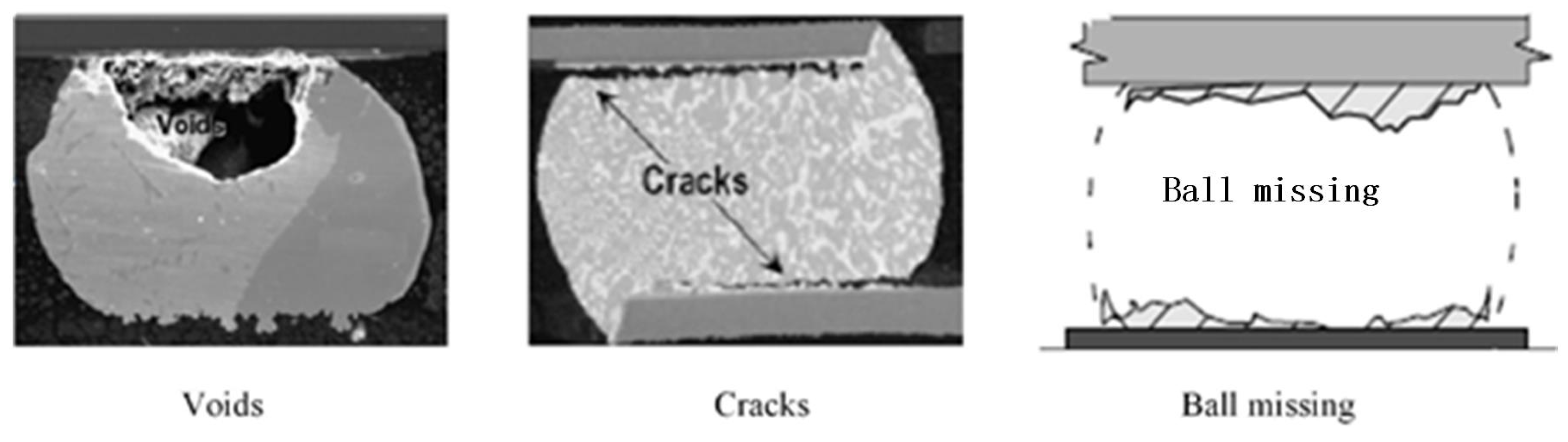
3]. At the same time, due to the lead-free materials used in the package and the internal structure of the chip in the packaging process, it is inevitable that thermal stress deformation and stress concentration happen, resulting in internal defects of solder balls, such as voids, cracks, ball missing and so on [
4,
5], as can be seen in
Figure 1. For ensuring the high reliability of internal connection, effective methods for non-destructively detecting the defects of flip chip are needed. A variety of techniques including
X-ray microscopy [
6], laser ultrasound [
7], active infrared thermal imaging [
8], vibration analysis [
9], and AMI (acoustic micro imaging) [
10,
11,
12] have been proven to be available for detecting the defects of interconnections in flip chip.
X-ray detection technology has been widely used in non-destructive detection of defects; however, this method requires expensive equipment, generates harmful radiation to the human body, and needs experienced operators. Shi et al. [
13] established a defect diagnosis system of flip chip based on active infrared detection technology, which can successfully distinguish the temperature difference between the ball missing and defect-free solder ball, and realized the defect of ball missing diagnosis and recognition. Active infrared thermal detection technology has a better effect on detecting flip chip with a larger solder ball size, but as the size of the solder ball of the flip chip further shrinks, the resolution of the infrared camera cannot meet the detection requirements. Compared with active infrared thermal imaging technology, AMI has the highest detection resolution up to the submicron level, which completely covers the detection range of the microsystem from the grain boundary, grain, and characteristic size to the whole microstructure [
14,
15,
16].
AMI technology is one of the most widely used techniques in the non-destructive testing of materials [
17]. High-frequency ultrasound for micro-defects diagnosis technology refers to acoustic micro imaging technology, which has been effectively applied to the detection of typical defects such as voids, cracks, and ball missing [
18]. It uses the high-frequency ultrasound emitted by the high-frequency focusing probe. The ultrasound wave propagates into the detected sample through the acoustic lens and the coupling medium-deionized water. When the acoustic wave is reflected, scattered, and transmitted at different interfaces within the object, the echo signal is received again through the probe. We can detect the position and size of micro defects in the object by comparing and analyzing both the time domain and frequency domain of a single point and the whole process echo signal carried out through the signal processing system [
19]. Hoh et al. [
20] used the MP and CP4 ultrasonic probes of 230 MHz to scan the same flip chip and obtained two ultrasonic images of the chip, and the chip defects are detected by image processing in a complementary way. This method can be used for the detection of solder ball cracks, but the image acquisition time is long, and the image processing is complex, so it is not suitable for online defect detection.
For the current ultrasonic detection system, due to the wave characteristics of acoustic waves, the focus is a circular region with a diameter close to the wavelength size. This phenomenon causes the problem of edge blurring of ultrasound image [
21]. In order to display the position, distribution, and size of micro defects intuitively, the sparse reconstruction of time-domain echo signals and the cross-section signals obtained by simulation is carried out to solve the effect of edge blurring in the imaging detection of micro defects [
22,
23]. The recognition and location of defects in the solder balls have been realized.
2. Principle and Methods of Sparse Representation
According to the theory of ultrasonic propagation, and considering the attenuation in frequency and shape change caused by the scattering of acoustic waves in different media, each reflected echo has a different shape. So, the model of ultrasonic echo signal is defined as:
where
represents the reflected signal propagating to the
ith interface.
refers to the reflection function, and
ε represents the noise from the test sample and the system. It can be seen that the accuracy of detecting the size and the location of defects in the ultrasonic testing process depends on the ability to describe the reflected echo information contained in the ultrasonic signal. As a result of the particularity of the object, the number of interfaces or defects is usually limited, the non-zero value only exists in several isolated locations in the time domain of reflection function
. That is, the reflection function is sparse, which provides the validity of sparse representation for the ultrasonic signal.
The sparse representation of signals refers to approximating the original signals with fewer basis functions (atoms). For a given ultrasound signal
y, sparse representation means that under a set of appropriate basis functions Q, the signal can have a set of corresponding decomposition coefficients
x. The sparse representation coefficient of signal
y is obtained by calculating:
where
denotes the
l0-norm of the vector
x to ensure the sparsity of solution.
D refers to the set of base functions
Q, i.e., dictionary
,
x represents the sparse decomposition coefficient of the signal, and
ε is the residue of coefficient representation. The set of atoms in the dictionary corresponding to non-zero elements in
x is the support set of the solution.
In order to make the shape of the atoms in the dictionary more similar to the signal and the support set smaller, the dictionary is usually extended into an over-complete dictionary. That is, the dictionary is composed of L atoms. The length of each atom is
N, where
N <
L. For the time-domain signal of ultrasonic echo, it is generally a broadband pulse signal centered on the probe frequency. The Gabor function can be used to make a complete description. When generating a complete dictionary based on the Gabor function, the dictionary contains many control parameters, and each atom in the dictionary can be represented by Equation (3):
where
represents a single atom,
S is a scaling parameter,
u is a translation parameter,
f is a frequency domain parameter, and
K is the amplitude parameter used for atom normalization. Values of
S,
u, and
f are determined by the reference echoes obtained from experiments. The surface echo signal is obtained as a reference echo by using a high-frequency ultrasound probe to detect a sufficiently large plane, and the echo is fitted by the Gabor model. The results are
= 0.67,
= 0.24, and
= 49.72 respectively.
Equation (3) is solved by the least squares orthogonal matching pursuit algorithm. The basic idea is to start with an empty set and construct an approximation of K terms by keeping a set of effective supporting set atoms. Then, we expand the solution set by adding one supporting set atom at each step. Each time the solution set is extended, the columns that can minimize the residuals are selected directly on the basis of the current support set, thus approaching y gradually. After each additional support set atom is approximated, the residual is recalculated, and the algorithm ends if the error is less than a certain threshold. The sparse representation of ultrasonic echo signals can enhance the resolution and signal-to-noise ratio of defect detection, thereby enabling the more accurate identification and localization of micro defects.
3. Simulation
In order to analyze the propagation mechanism of an ultrasonic wave in a complex chip and the energy distribution of an ultrasonic wave acting on a chip micro defect more intuitively, the ultrasonic detection of flip chip is simulated by the “Acoustic-Solid Interaction, Transient” in COMSOL Multiphysics. The ultrasonic echo signal is obtained by simulation. The one-dimensional and cross-section sparse reconstruction of ultrasonic echo are carried out to improve the efficiency and accuracy of testing for micro defects.
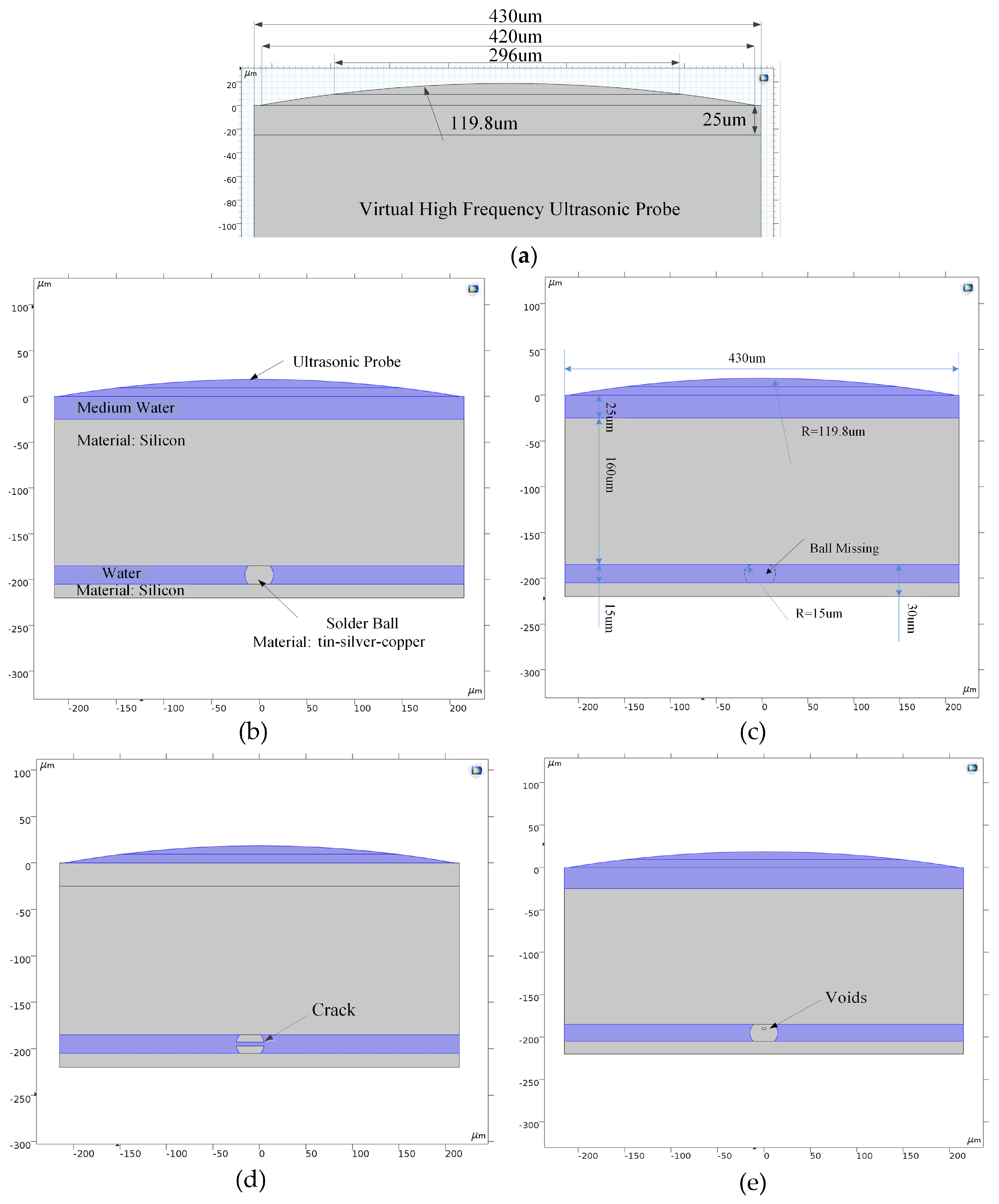
In order to reduce the amount of calculation in the simulation process, the Sonoscan 230SP probe(D9500, Sonoscan, Elk Grove Village, IL, USA) is scaled down according to the principle of equal scale reduction. The size of the probe model is shown in
Figure 2a. According to the principle of COMSOL modeling and the reality of the flip chip, three typical defects of flip chip solder balls and a normal one are simulated. The parameters in the model are taken from the material database of COMSOL software as shown in
Table 1, and the models are shown in
Figure 2.
According to the principle of modeling, the “Pressure Acoustics, Transient” module and “Solid Mechanics” module are introduced into COMSOL. For the pressure acoustic module, an inward normal displacement (Gabor function, length of 10 ns) is loaded on the incident arc to simulate ultrasound. The Gabor function can be described as:
At the same time, for the solid mechanics module, the solid boundary is set as a “low reflection boundary” to simulate the linear elastic material characteristics used in the simulation. The interfaces of micro defects are set as the acoustic–solid coupling boundary. According to the operation speed of the personal computer, the free triangular mesh is used for gridding operation in the model, and a wavelength of 6 grids is set. The simulation is carried out in two steps and the step size is set to T0/20. Firstly, the normal displacement is loaded on the probe for 20 ns, which is used as the condition of the Study 1 structure of COMSOL simulation. After 20 ns, the excitation signal is removed, and the boundary condition of the normal displacement is modified to the scattering boundary. This process lasted for 110 ns as a condition for Study 2. The sound pressure measured in the region where the probe center frequency located is integrated and processed as the received signal.
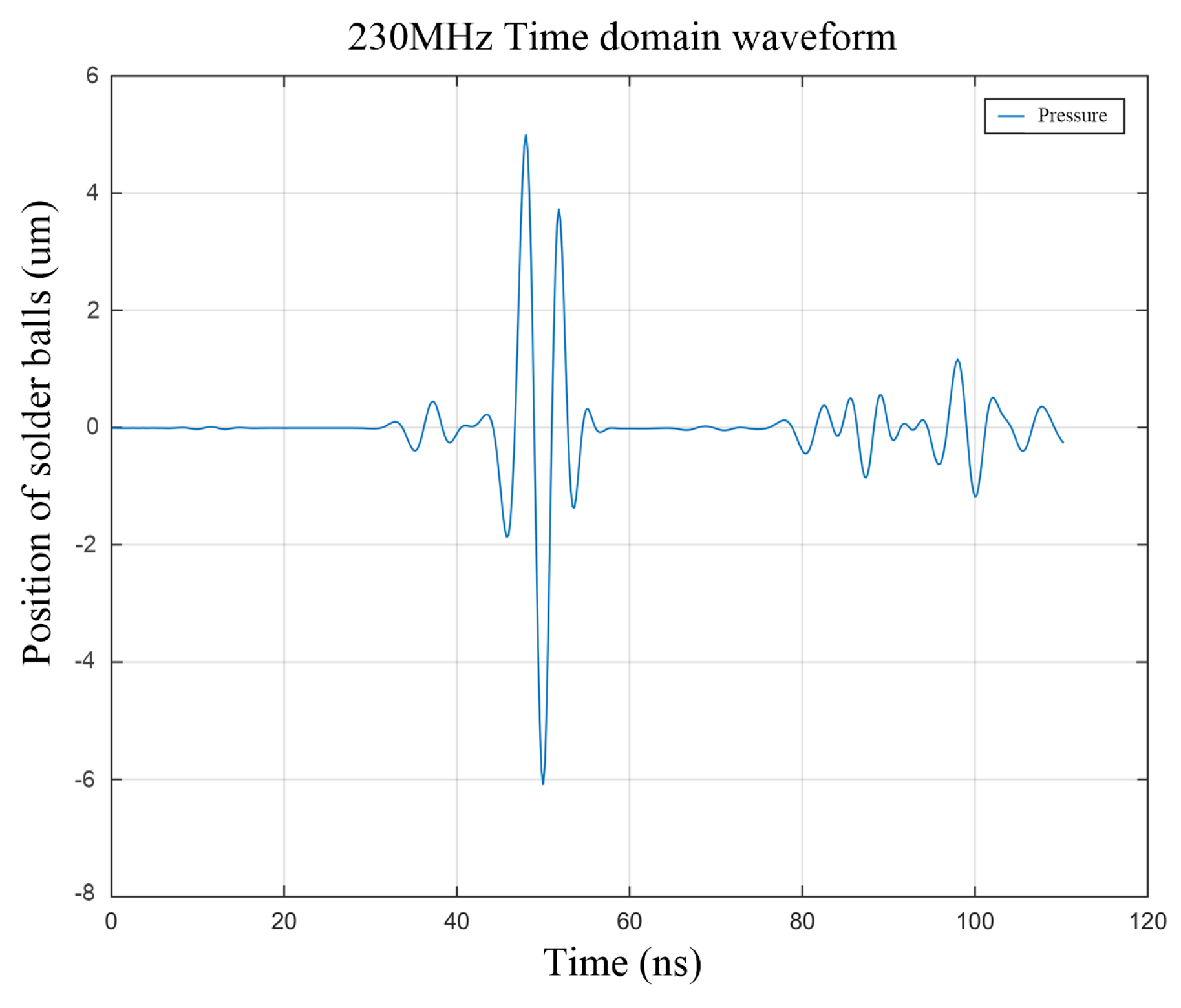
The time-domain signal graph of an ultrasound, namely the A-scan, is obtained by simulating the void defect detection of solder balls. The A-scan graph is shown in
Figure 3. The first signal peak in
Figure 3 is the echo signal of the upper surface (the interface of water and silicon). The second signal peak is the echo signal of silicon and the tin–silver–copper interface. The third signal peak is the echo signal of tin–silver–copper and the void interface. The energy attenuation caused by transmission and refraction occurs at the interface of acoustic impedance, so the signal peak behind is smaller. The reason why the amplitude of the second signal peak is smaller than that of the third one is that the acoustic impedance between silicon and tin–silver–copper is smaller, so the ultrasonic reflection at the second interface is weaker and the signal peak reflected in the figure is smaller.
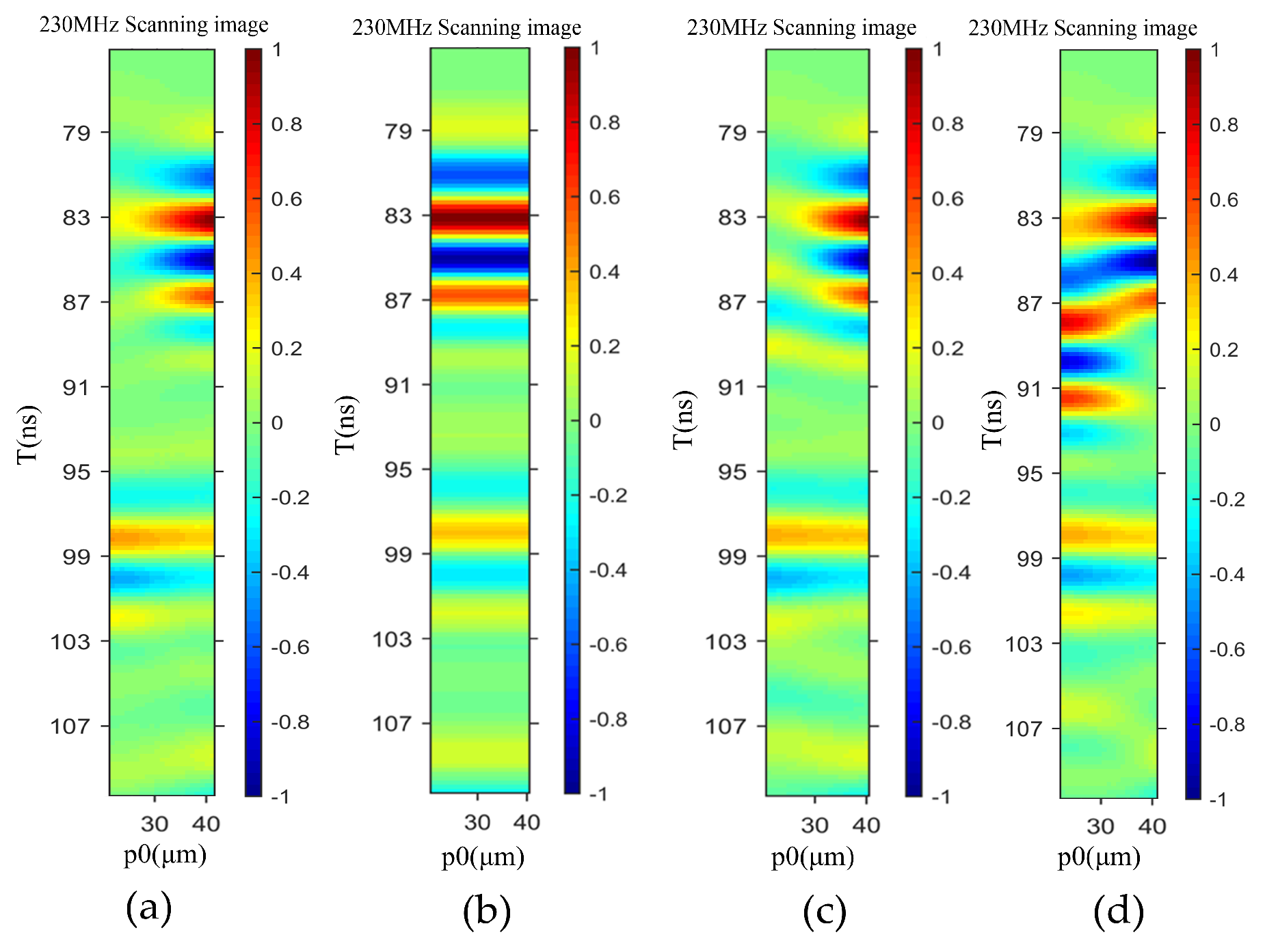
The change process of the relative position between the solder ball and the ultrasonic probe was simulated by modifying the position of the solder ball. At the beginning of the simulation, the virtual probe is located directly above the center of the micro defect, and then the position of the micro defect moves in a step of 1 μm to simulate the whole process of the ultrasonic probe scanning solder ball. When a solder ball moves 1 micron, it will be simulated once. The simulation moved a total of 40 μm and obtained 41 transient simulation results. Combining all of the transient simulation results, the A-scan signal, in a similar B-scan mode, results in a B-scan image of the typical defects of the solder balls, as shown in
Figure 4.
Comparing all the four different defect diagrams, it can be seen that the energy distribution of the four diagrams is obviously different between 75 and 95 ns, as shown in
Figure 5. This phenomenon also denotes that the ultrasonic echo of typical defects of solder balls is within the time threshold. At the same time, comparing the four B-scan diagrams in
Figure 4, we can see that the acoustic pressure energy near 50 ns is the highest, which is consistent with the phenomenon that the highest reflection energy occurs at the interface of water and silicon, which is caused by the reflection and transmission of the ultrasonic energy at each acoustic impedance interface.
Figure 5a shows the B-scan image of a defect-free solder ball. Within the time threshold 75–110 ns of the defect, it can be seen that the ultrasound echo amplitude in the area of 0–15 microns at the position of P0 is obviously less than that in the area of 15–40 microns. This is because the acoustic impedance of the silicon and tin–silver–copper interface is smaller than that of silicon and the water interface, which results in the ultrasonic energy of transmission and refraction occurring in the region of the radius of the solder ball within 15 microns, and the ultrasonic energy and amplitude of reflection are smaller.
As can be seen from the B-scan image of the ball missing in
Figure 5b, the energy expressed at 0–40 microns is the same, because the interface passed by ultrasound is the silicon and dielectric water interface at the position of 0–40 microns.
For the B-scan image of void defect in
Figure 5c, it can be seen that the ultrasonic amplitude (yellow–blue–yellow) in 87–90 ns time domain is arc-shaped, because the void defect in solder balls is oval. However, the void in solder balls is very small, and the difference between the B-scan image and the image without defects is not particularly obvious.
For the crack defect in
Figure 5d, because the crack is located on the middle cross-section of the solder ball and the filling medium is water, it can be seen that within the time threshold 80–85 ns, the ultrasonic reflection amplitude is less than the ultrasonic amplitude within 87–92 ns at the position of 0–15 microns. This is because the ultrasound experiences two interfaces during this time, namely the interface of silicon and tin–silver–copper and the interface of tin–silver–copper and water. The ultrasonic amplitude at the position of 15–40 is consistent with the amplitude in
Figure 5a,c.
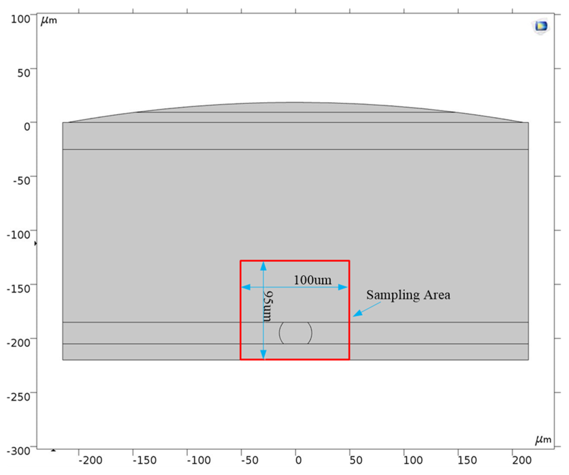
To observe the sound wave transmission, reflection, and refraction during the sound propagation process, the sound wave propagation process in the entire time domain was integrated into one image, the acoustic propagation map, which can realize better analysis of the acoustic energy distribution around the micro defects. In order to highlight the changes in the energy of sound waves of the micro defects caused by ultrasound, we further extract and focus the scan results. The sampling area is shown in
Figure 6. The adopted area was under the probe in the different probe detection positions. The abscissa of area is (−50 μm, 50 μm), and the ordinate is (−125 μm, −220 μm). The space sampling interval is set as 1 μm, and the sampling time interval was set as 0.2 ns ranging from 20 to 50 ns according to the speed of calculation and the law of ultrasonic propagation in the model.
For the analysis of ultrasonic energy distribution, we extracted the transient value of displacement for the solid region and the pressure value for the liquid region in the sample. The displacement and pressure data of each defect location are extracted and converted into energy values. In the solid region, the square of the displacement value at this position has a linear relationship with the acoustic energy. In the liquid region, the absolute value of the pressure at the position has a linear relationship with the acoustic pressure, so the matrix of the acoustic energy can be expressed by
. The size of the matrix is 101 × 96. The acoustic energy peak path map (AEPPM) can be obtained by processing the maximum value of the matrix along the time axis, and the expression can be described as,
where
disp represents the displacement value of the position in the solid area,
p_
t denotes the pressure of the position in the liquid area,
x,
y is the geometric coordinate position, and
t represents the number of steps when extracting data. The AEPPM of different defects in flip chip solder balls are shown in
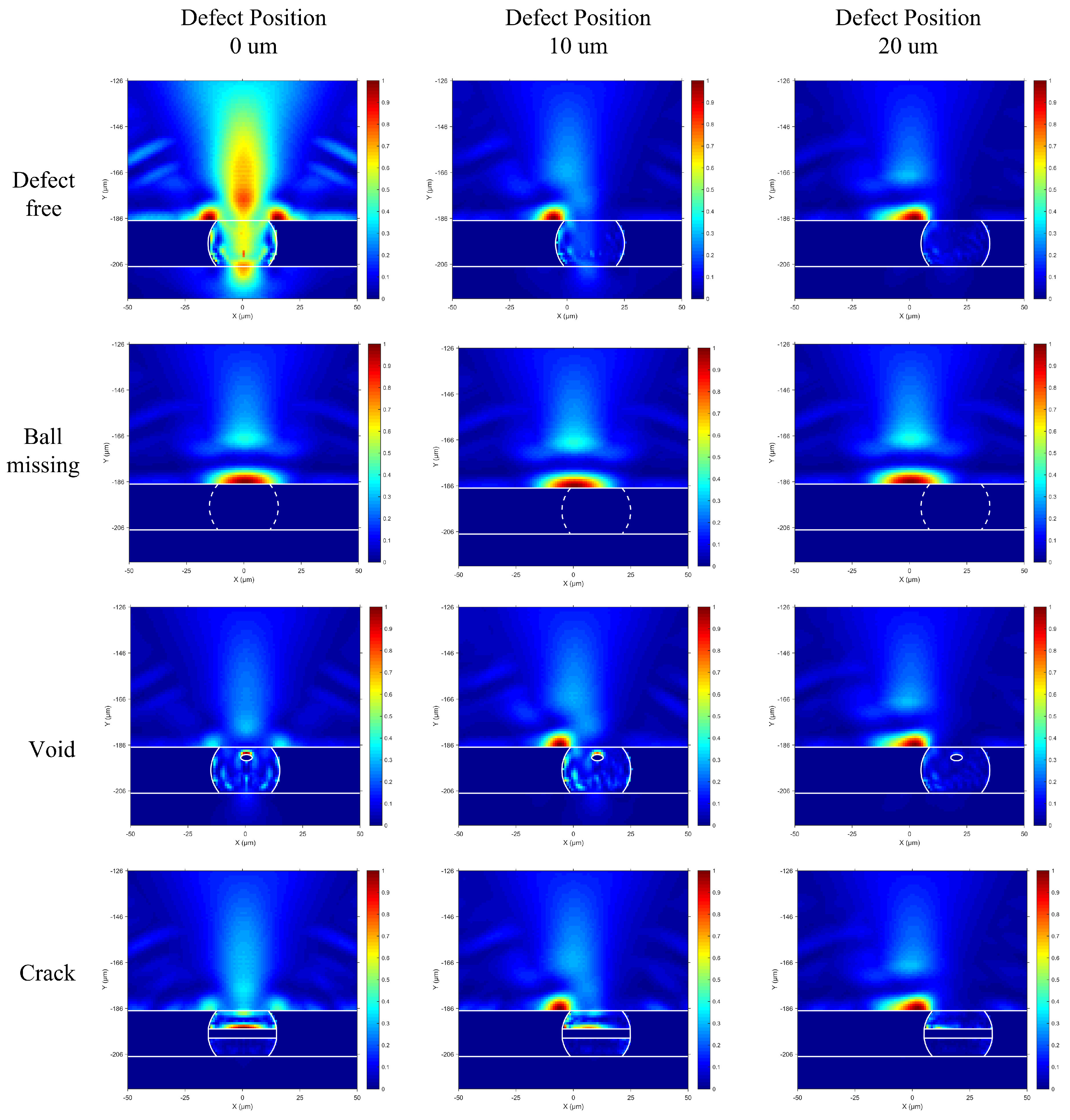
Figure 7.
By comparing and analyzing four typical solder balls in different defect positions in
Figure 7, it can be seen that the energy transmitted into the solder ball by ultrasound in the defect-free model is much stronger than that of the other three solder balls when the defect of the solder ball is at 0 μm. This is because the acoustic impedance of the interface between silicon and tin–silver–copper is smaller than that of the other three defect interfaces (the interface of silicon and water, the interface of tin–silver–copper and air, and the interface of silicon and water), so there will be a significant energy difference in the peak plot. As the position of the defect moved to 10 μm, the acoustic energy has a significant reflection on the left side of the upper surface of the void model, defect-free model, and crack model. However, the energy transmission of ball missing does not change with the movement of the solder ball, which can be seen from the red area in the figure. At the same time, the energy peak of the three kinds of defects, except for the ball missing, propagates downward along the left side of the solder ball through transmission. As the defect position continues to move, it can be seen that the acoustic energy transmitted into the solder ball is significantly reduced to disappear. The AEPPM can show the propagation path of the energy peak, as well as the information of the acoustic amplitude and propagation direction.
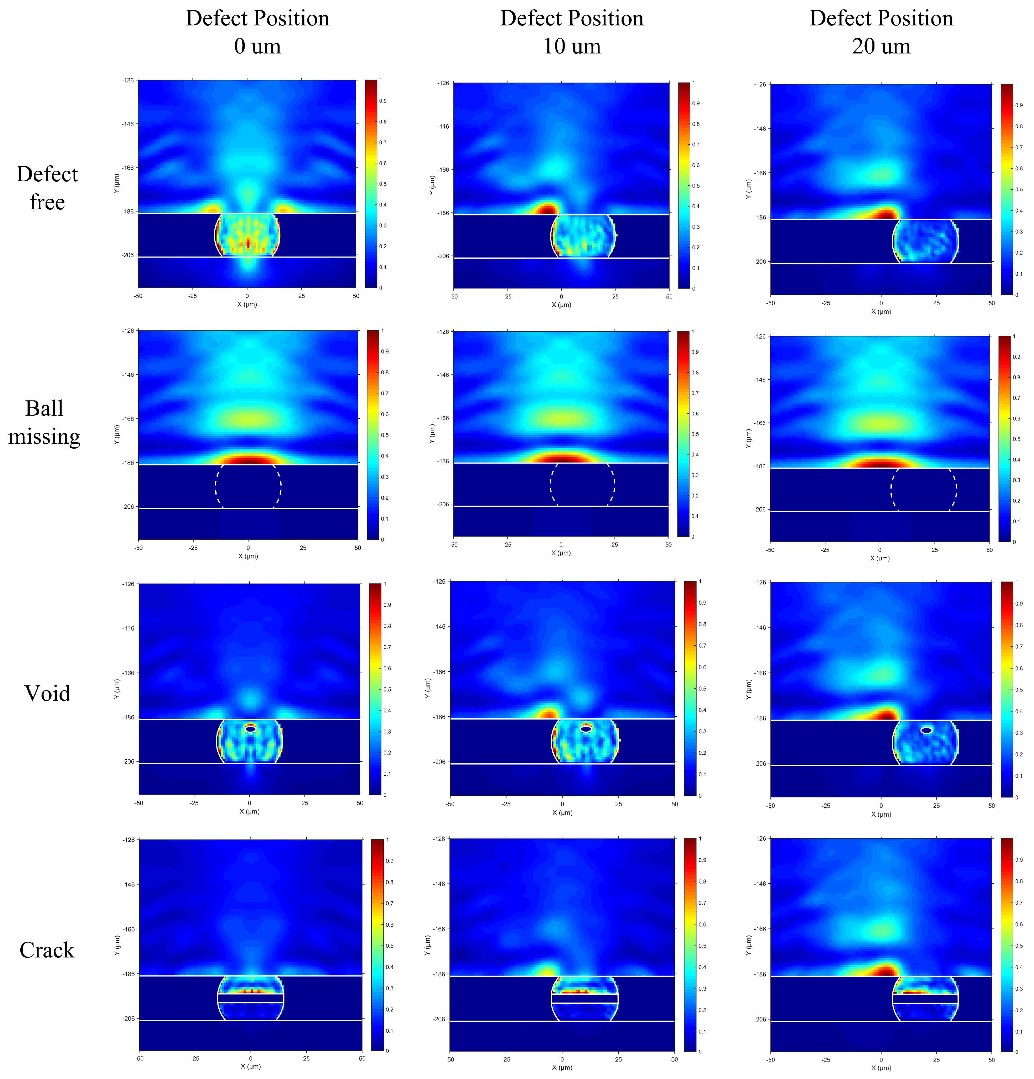
In order to further analyze the ultrasonic energy, we also observed the acoustic energy flux map (AEFM). The AEFM sums up the displacement matrix and pressure matrix in the region. The corresponding AEFM can be obtained by summing up the acoustic energy matrix along the time dimension, which can be described as
According to the time step, the displacement matrix and pressure matrix of each time point are summed to get the AEFM, which is shown in
Figure 8.
By comparing four different ball defect AEFMs and comparing them with AEPPMs, it can be seen that AEFM has more folds under the probe of the same model than AEPPM. This is due to the superposition of acoustic reflection energy and incident energy in AEFM, which results in the energy inconsistency in each position. While the incident energy of AEPPM is larger than the reflected energy, and only the peak energy of this position is taken, it appears more continuous and smooth in the map. Compared with AEPPM, for voids, AEFM can better see that the energy transmitted by the ultrasound into the solder ball and the voids have strong reflections, which can be clearly seen from the red spots on the upper surface of the voids. This is because the acoustic impedance formed by the air in the void and the solder ball is very large, so there is a clear red reflection area above the void. The other energy distribution is consistent in the two maps.
3.1. Sparse Representation of One-Dimensional Ultrasound and Echo Signal
In this paper, a structured dictionary is constructed based on Gabor function, and the least squares orthogonal matching algorithm is used to characterize ultrasound. The results show that the algorithm has good representation for one-dimensional time domain signals and cross-section images.
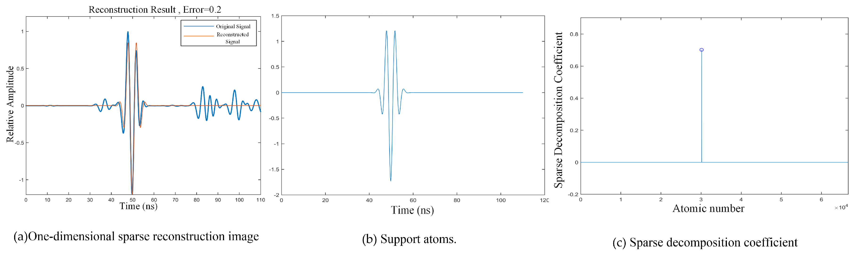
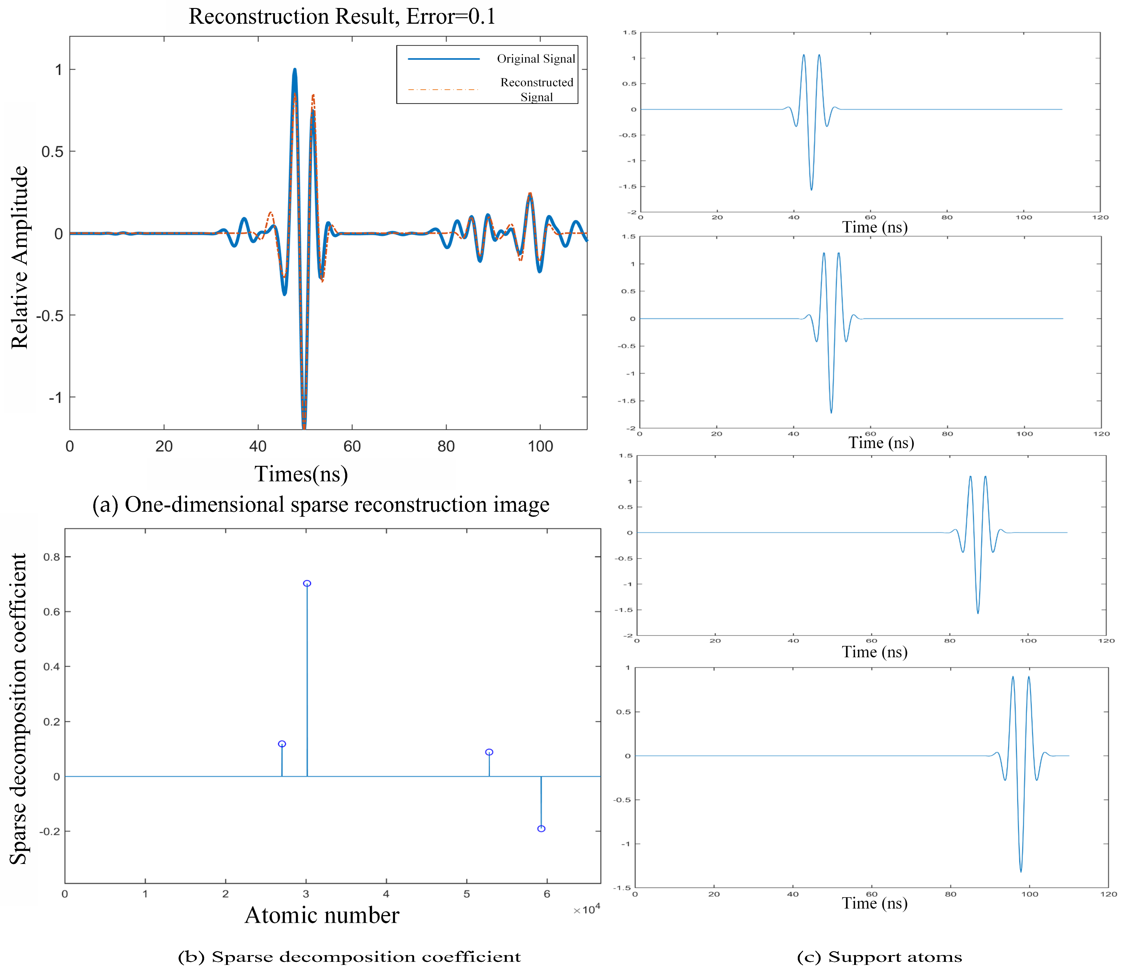
There will be different sparse representation results when setting different residual thresholds. The corresponding sparse representation results of residual 0.2 are shown in
Figure 9. As can be seen from the figure, the sparse reconstructed signal only fits one echo signal, and there is only one corresponding support set atom and only one sparse decomposition coefficient. This means that among all the atoms in the dictionary, only one sparse decomposition coefficient is non-zero, and the signal in the time domain of 80–110 ns is not fitted.
When the set threshold residual is 0.1, the sparse reconstruction image is much better than the threshold of 0.2. It not only removes the noise, but it also removes the echo signal inside, as shown in
Figure 10. There are four atoms in the support set, in which each atom corresponds to an echo, and the position of the atoms in the support set is exactly the same as that of the echo signal. From
Figure 10b, we can see that three of the four atoms in the support set are positive and one is negative, which means that the echo corresponding to the negative coefficient is opposite to that of the atoms in the support set. By comparing the four sparse decomposition coefficients, we can see that the larger the absolute value of the sparse decomposition coefficient, the larger the amplitude of the reflected signal at the location and the stronger the signal intensity.
3.2. Sparse Representation of Typical Defect Section Image
Cross-section reconstruction is a method used to further improve the computing speed on the basis of the previous sparse reconstruction of one-dimensional images. The difference between cross-section reconstruction and one-dimensional image reconstruction is that section reconstruction is the basis for judging the end of our final iteration method by simultaneously controlling the number of supporting set atoms and setting the threshold of residual error. The sparse reconstruction of a one-dimensional image only uses the residual threshold to control the number of supporting set atoms. By further controlling the number of supporting set atoms, we can ensure that the number of supporting set atoms we get is neither too much nor zero. In this way, we can ensure the stability of the computing speed on the basis of being closer to the original signal.
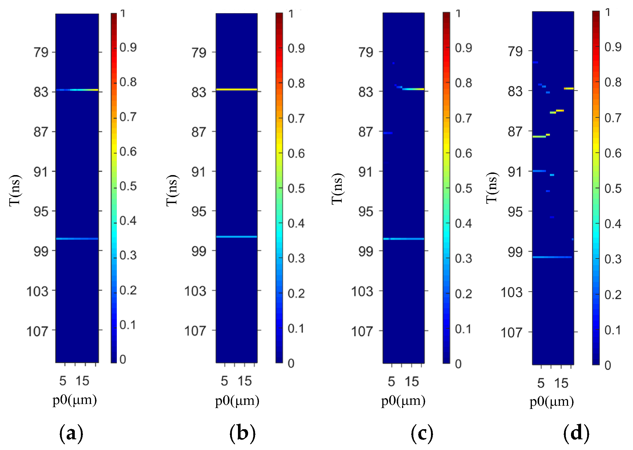
The sparse characterization of the typical defect signals in the time domain and the results of the sparse characterization coefficients are arranged and combined according to the location of the defects detected. The results are shown in
Figure 11.
By analyzing and comparing the sparse coefficient diagrams of each kind of solder ball defects, there are obvious coefficients near 83 and 99 ns in the four images, which is exactly the reflection phenomenon of the ultrasonic wave passing through the upper and lower surfaces of the solder ball. For the void defects of the solder ball in
Figure 11c, there are sparse values near 87 ns, which confirms that the location of the void of the solder ball is in just the right place at the time of modeling. The coefficients of the voids are smaller than those of the other interfaces. This is because when the ultrasound encounters the void defects, not only does the reflection occur, but there is also diffraction along the edge and below the voids, which results in the smaller value of the coefficients due to the reflection energy of the ultrasound.
For
Figure 11a, the absolute value of the decomposition coefficient at the position of P0 between 0 and 15 microns is smaller than that at the position of 15–20 microns near 83 ns. The reason is that the interface of silicon and tin–silver–copper occurs at the position of 0–15 microns, while the interface of silicon and water occurs at the position of 15–20 microns. Since the acoustic resistance of the latter is larger, the emission energy of an ultrasound that occurs at the interface is more, and the absolute value of the sparse characterization coefficient is larger.
For the ball missing defect in
Figure 11b, the two interfaces with obvious reflection are the silicon–dielectric water and dielectric water–silicon interfaces, while the sparse decomposition coefficient of the latter is smaller than that of the former because the energy of transmission into the lower interface decreases due to the emission of ultrasound in the process of propagation from top to bottom.
For
Figure 11d, the value of the sparse decomposition coefficient of the ultrasound exists at the time of 83 ns, 88 ns, and 91 ns during the position of 0–15 microns, and the coefficient at 88 ns is the biggest. It is due to the ultrasound reflections at the upper surface of the crack (the interface of tin–silver–copper and water), which demonstrates that the crack defect is located at the time of 88 ns. According to the velocity of ultrasound in the material, we can calculate the location of the defect. What’s more, according to the length of the coefficient along the P0 direction, the size of the crack is obtained. However, because the time difference between the reflection of the upper surface of the defect and the edge of the solder ball is very small, the echo emission overlaps. So, at 85 ns, there are values of sparse reconstruction. As a result of the presence of crack defects, the obvious reflection and refraction happen multiple times, which results in the coefficient values of sparse reconstruction existing in other time domains. These phenomena may cause misjudgment about defects. There is still work that remains to be done.


