Article

Preliminary Study on the Model of Thermal Laser Stimulation for Defect Localization in Integrated Circuits

1
National Space Science Center, Chinese Academy of Sciences, Beijing 100190, China
2
School of Astronomy and Space Science, University of Chinese Academy of Sciences, Beijing 100049, China
3
School of Electronic, Electrical and Communication Engineering, University of Chinese Academy of Sciences, Beijing 100049, China
*
Author to whom correspondence should be addressed.
Appl. Sci. 2020, 10(23), 8576; https://doi.org/10.3390/app10238576
Submission received: 1 November 2020 / Revised: 23 November 2020 / Accepted: 25 November 2020 / Published: 30 November 2020
(This article belongs to the Special Issue Multiscale Modelling of Laser-Induced Phenomena on Solids)

Abstract

:
Thermal Laser Stimulation (TLS) is an efficient technology for integrated circuit defect localization in Failure Analysis (FA) laboratories. It contains Optical Beam-Induced Resistance Change (OBIRCH), Thermally-Induced Voltage Alteration (TIVA), and Seebeck Effect Imaging (SEI). These techniques respectively use the principle of laser-induced resistance change and the Seebeck effect. In this paper, a comprehensive model of TLS technology is proposed. Firstly, the model presents an analytical expression of the temperature variation in Integrated Circuits (IC) after laser irradiation, which quantificationally shows the positive correlation with laser power and the negative correlation with scanning velocity. Secondly, the model describes the opposite influence of laser-induced resistance change and the Seebeck effect in the device. Finally, the relationship between the current variation measured in the experiment and other parameters, especially the voltage bias, is well explained by the model. The comprehensive model provides theoretical guidance for the efficient and accurate defect localization of TLS technology.

1. Introduction

With the scaling down of the integrated circuit process and the increase of the metal layers, circuit-level defects are more and more difficult for an optical microscope to observe. Therefore, nondestructive Failure Analysis (FA) for Integrated Circuits (IC) has gradually become necessary. Defect localization is a fundamental step in FA. Accurate and efficient localization makes a great contribution to the analysis of the failure’s physical causes. At present, several optical based technologies, such as Emission Microscopy (EMMI), Photoelectric Laser Stimulation (PLS), Thermal Laser Stimulation (TLS), and Laser Voltage Probing (LVP), have been proven to meet the present requirements [1]. Among all the advanced technology, TLS is an efficient and non-destructive method used in back-side localization [2,3,4]. TLS technology has proved that it is sensitive to leakage current [5], short-circuit [3], and open-circuit [6]. It is applicable to metallic, polysilicon, and highly doped silicon structures [7]. However, TLS still has some limitations. Because of the high reflectivity of the metal layer to the laser, it is difficult for TLS to locate a defect at a deep level [8]. In 2017, a modified technology called Lock-in TLS was proposed to locate the defect in multilevel interconnects [9].
TLS technology contains three techniques, Optical Beam-Induced Resistance Change (OBIRCH), Thermally-Induced Voltage Alteration (TIVA), and the Seebeck Effect Imaging (SEI). OBIRCH was firstly proposed by Nikawa et al. [10], while TIVA and SEI were proposed by Edward I. Cole Jr. [11]. A simulation model of OBIRCH and TIVA was proposed in 2001 [12]. In 2005, reports showed that the SEI signal would be affected by the OBIRCH signal in experiments [13,14]. The three techniques mentioned above are used in different test situations. Each technique has its unique test mechanism. However, the comprehensive theoretical model of TLS technology is still deficient.
In this paper, a comprehensive model of TLS technology is proposed. This model describes the whole process of the laser beam interacting with the IC and the joint influence of the laser-induced resistance change effect and Seebeck effect. Next, a defect localization and analysis experiment is carried out. The experimental results are consistent with the predictions of the theoretical model. The comprehensive model provides theoretical guidance for the efficient and accurate defect localization of TLS technology.

2. TLS Principle

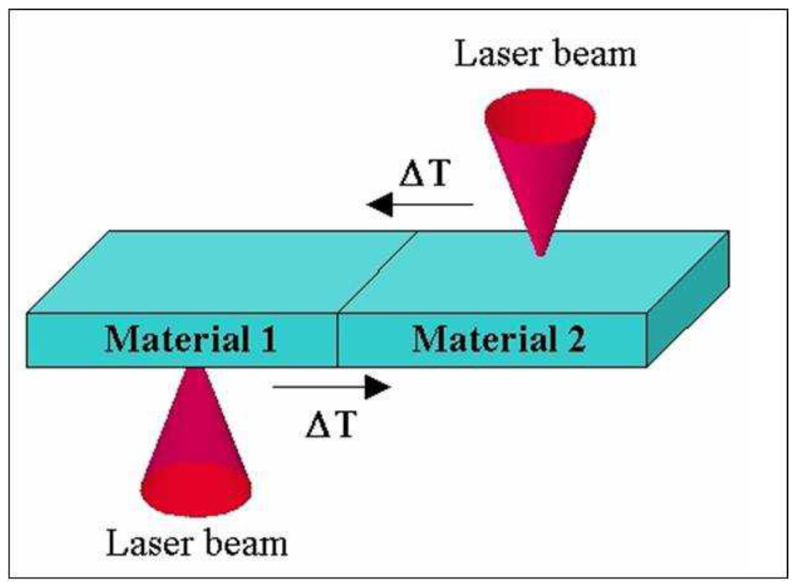
2.1. Classical Model

Because of the reflection of the front-side metal layer, it is difficult for the laser to reach deep levels from the front side of the device. Backside laser irradiation has proven to be an effective method [8,11]. In TLS, a continuous infrared laser (wavelength of 1.3 μm) is used to scan the back-side silicon substrate for two reasons,
  • The photon’s energy for the 1.3 μm infrared laser ( h c λ 0.95 eV) is lower than the silicon band gap energy (1.12 eV), so the laser hardly generates a photo-current [10];
  • Silicon is almost transparent at such a wavelength, so the laser beam can reach the active area through the back-side substrate at low loss [11].
It is well known that thermal energy leads to an increasing temperature Δ T , causing a variation of resistivity:
Δ ρ = ρ 0 α TCR 2 δ r Δ T
where ρ 0 , α TCR , and δ r are respectively the electrical resistivity, the Thermal Coefficient of Resistivity (TCR), and the thermal expansion coefficient of the material. δ r is so small relative to α TCR that it is negligible in most cases [15]. The resistivity and temperature coefficients of some metal materials are shown in Table 1.
In the OBIRCH technique, a constant voltage bias V 0 is applied to the Device Under Test (DUT) [12]. Due to the changed resistance, the current Δ I varies as:
Δ I Δ R R I = Δ R R 2 V 0
where Δ R is the resistance variation and I is the current of the DUT before laser irradiation. In the TIVA technique, however, a constant current bias I 0 is used [12]. The variation of the voltage Δ V is:
Δ V Δ R R V = I 0 Δ R
where V is the voltage of the DUT before laser irradiation.
The SEI technique, which typically uses zero-bias or constant current bias, is based on the so-called Seebeck effect. While two contiguous materials have different temperatures (see Figure 1) [7], a Seebeck voltage is generated according to the following equation:
Δ V S S 1 S 2 Δ T = S 1 2 Δ T
where Δ T is the temperature difference between two materials and S 1 2 = d V d T is the Seebeck coefficient. Seebeck coefficients for several materials or junctions are presented in Table 2. It can be positive or negative in different contacted materials. The Seebeck voltage is independent of the circuit resistance, and it has an effect on the voltage or current of the circuit.

2.2. Comprehensive Model

The rationales for all three techniques have been proposed; however, these effects occur simultaneously in the circuit, and the results they produce interfere with each other. Therefore, it is necessary to establish a comprehensive model of TLS technology to research for the proportion of each effect on the circuit.

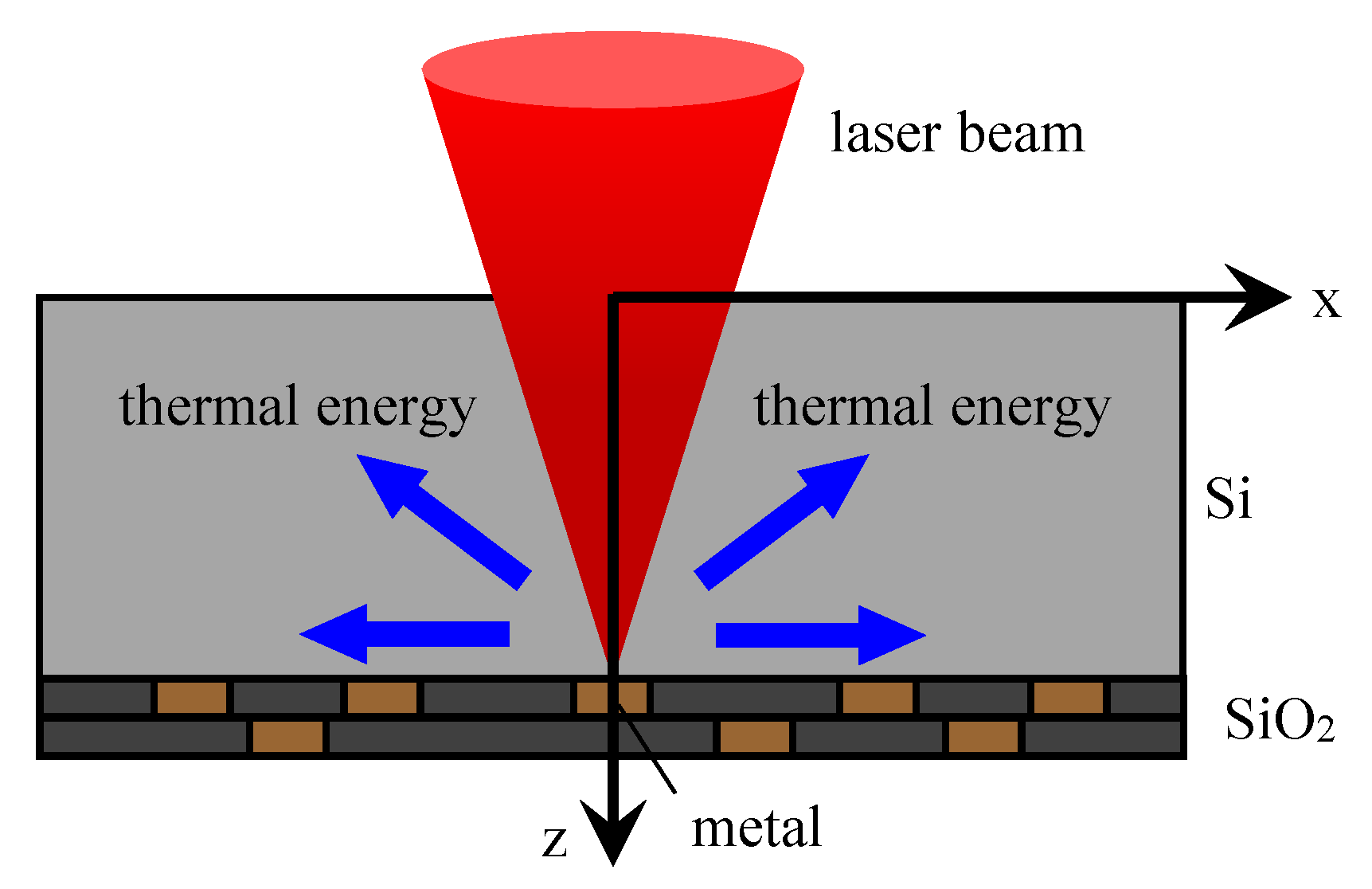
2.2.1. The Evolution of the Temperature Field in the Circuit after Laser Irradiation

When the laser beam is focused on the active area of the DUT (see Figure 2), a temperature field is generated, following the thermal conduction equation:
ρ c T t κ 2 T = Q ( x , y , z , t )
where ρ , c, and κ are respectively the density, heat capacity, and thermal conductivity of the material. Q ( x , y , z , t ) , as a function of position ( x , y , z ) and time t, is the heating source produced by the laser beam. Taking the case of a laser beam moving along the positive x direction as an example, the expression of Q is:
Q ( x , y , z , t ) = 1 R P 0 π γ ω 2 ( z ) exp x v t 2 + y 2 ω 2 ( z ) z γ
where P 0 , ω 2 ( z ) , R, and γ are respectively the power, spot size, reflectivity, and attenuation length of the laser. v is the scanning velocity of the laser spot. Equation (6) uses the approximation of the Gaussian intensity profile [15].
In general, the temperature variation in the xy plane is what we are interested in. Besides, the area of the IC layout is much larger than that of the laser spot. Therefore, the model mentioned above can be transformed into the temperature field distribution in two-dimensional infinite space. Equations (5) and (6) are converted to:
ρ c T t κ 2 T x 2 + 2 T y 2 = Q ( r , t )
Q ( r , t ) = 1 R P 0 π γ ω 2 exp x v t 2 + y 2 ω 2
where r = ( x , y ) . In Equation (8), the laser spot size ω 2 is treated as a constant. Considering that the temperature difference Δ T = T T 0 is also a special solution to Equation (7), the boundary condition is:
Δ T ( r , t ) | r = 0 , Δ T ( r , t ) | t = 0 = 0
Equation (7) can be solved by a Green’s function approach [17] to give:
Δ T ( r , t ) = 0 t d t Σ G ( r , t ; r , t ) Q ( r , t ) d r
where Σ is the whole two-dimensional plane and G ( r , t ; r , t ) is the Green’s function for point excitation at ( r , t ) given by:
G ( r , t ; r , t ) = 1 4 π k t t exp x x 2 + y y 2 4 k t t η ( t t )
where k = κ ρ c and η ( t t ) is the step (Heaviside) function. Using Equations (8) and (11) in Equation (10), we can obtain:
Δ T ( r , t ) = 1 R P 0 4 π ρ c γ 0 t 1 ω 2 + 4 k t t exp x v t 2 + y 2 ω 2 + 4 k t t d t

2.2.2. The Variation of the Current or Voltage in the Circuit

When the laser beam is focused on the abnormal spot or the normal spot of the DUT, a temperature variation Δ T that meets Equation (12) is formed. The variation of resistance Δ R and the Seebeck voltage Δ V S are respectively:
Δ R = Δ ρ d l A = ρ 0 α TCR Δ T A d l
and:
Δ V S = S 1 2 ( Δ T ) · d l 1 2
where d l 1 2 is a tiny length in the direction of the current flowing, A is the cross-sectional area, and ( Δ T ) · d l 1 2 is the temperature difference between the two contact materials. At the abnormal spot of the failed device, thermal diffusion is more difficult, so the local temperature is much higher. Therefore, the values of Δ R and Δ V S are bigger than those at the normal spot. The difference can be detected by testing the current or voltage.
As for a device under constant voltage bias V 0 , Δ R and Δ V S will cause a variation of the current. The value of current variation Δ I is:
Δ I = I TLS I = V 0 + Δ V S R + Δ R V 0 R
where V 0 is the voltage bias, I 0 is the current before the laser irradiation starts, and R is the resistance of the DUT [14]. The laser power used in the experiment is less than 100 mW, resulting in very small Δ R and Δ V S . Therefore, Equation (15) is approximated to:
Δ I = Δ V S R + Δ R + V 0 R + Δ R V 0 R Δ V S R V 0 R 2 Δ R
There are two parts on the right of Equation (16), the first of which is mainly contributed by the Seebeck effect, and the second is dominated by laser-induced resistance change. Therefore, the OBIRCH and SEI techniques coexist in a test. While V 0 is equal to a critical value V c , Δ I will be equal to zero. From Formula (16), the value of V c is:
V c = Δ V S Δ R R
When V 0 > V c , Δ I < 0 , that is the OBIRCH technique dominates. Otherwise, the SEI dominates.
While constant current bias I 0 is applied, the TIVA and SEI will coexist, and the voltage variation Δ V is:
Δ V = V TLS V = I 0 R + Δ R Δ V S I 0 R = Δ V S + I 0 Δ R
The contributions of the two effects are still opposite. Besides, a critical current bias I c that causes Δ I = 0 is [14]:
I c = Δ V S Δ R
When I 0 > I c , Δ V > 0 , and the TIVA technique dominates. When I 0 < I c , the SEI dominates. Therefore, the SEI technique always requires low bias conditions.
For an active device, according to [14], an extra weak current I PN exists after laser irradiation, which is preliminarily interpreted as a light-current signal. I PN has little influence on the current variation Δ I or voltage variation Δ V .

2.2.3. The Comprehensive Model

Combining the conclusions of Section 2.2.1 and Section 2.2.2, the relationship between the values measured in TLS technology and the experimental parameters is established. In constant voltage bias, the current variation is:
Δ I C 1 P 0 R S 1 2 f ( x , y , v , t ) · d l 1 2 C 1 P 0 V 0 R 2 ρ 0 α TCR A f ( x , y , v , t ) d l
In constant voltage bias, the voltage variation is:
Δ V = C 1 P 0 S 1 2 f ( x , y , v , t ) · d l 1 2 + C 1 P 0 I 0 ρ 0 α TCR A f ( x , y , v , t ) d l
where:
C 1 = 1 R 4 π ρ c γ , f ( x , y , v , t ) = 0 t 1 ω 2 + 4 k t t exp x v t 2 + y 2 ω 2 + 4 k t t d t
The meaning of each consideration is already explained in the content above. Equations (20) and (21) entirely describe the principle of TLS technology. They correlate the measurable quantities (current variation Δ I and voltage variation Δ V ) with adjustable quantities (laser power P 0 , scanning velocity v, and bias conditions V 0 / I 0 ).
The structure and material composition of actual ICs are complex. Therefore, the evolution of the temperature field with time also varies with different materials and structures. However, the predictions of the comprehensive model are still in good agreement with the experimental results.

3. Experiment and Discussion

3.1. Experiment Setup

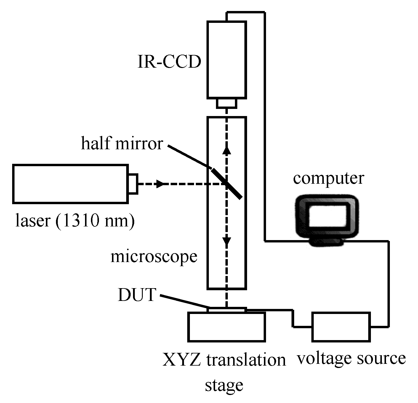
3.1.1. Testing System

In order to verify the comprehensive model, a defect localization experiment is performed using the Laser Scanning and Testing System (LSTS; see Figure 3) at the National Space Science Center, Chinese Academy of Sciences. The relevant parameters of the facility are shown in Table 3. The computer is used to monitor the current. As the laser beam scans the defect location, the abnormal Δ I will be tested, and a red spot will be marked on the layout diagram. The test results supplied by the voltage source or current source have similar properties according to Equations (16) and (18), so a voltage source is used for the test.

3.1.2. DUT

The tested device sample is a Micro Control Unit (MCU; see Figure 4a), which is a computer system integrated on a chip. After functional testing, the failure area is located in the red box in Figure 4a. When the normal sample is power supplied with no function running, the supply voltage V 0 is situated in the range of 1.8∼3.6 V. The typical value of the current I 0 is 1.4 μA when V 0 = 3.3 V.
The fail sample has a leakage current (Figure 4b), the typical value of which is I 0 = 595 μA at V 0 = 3.3 V. This current value is much larger than that of the normal device. As the supplied voltage increases, the current increases, and the resistance decreases.

3.2. Results and Discussion

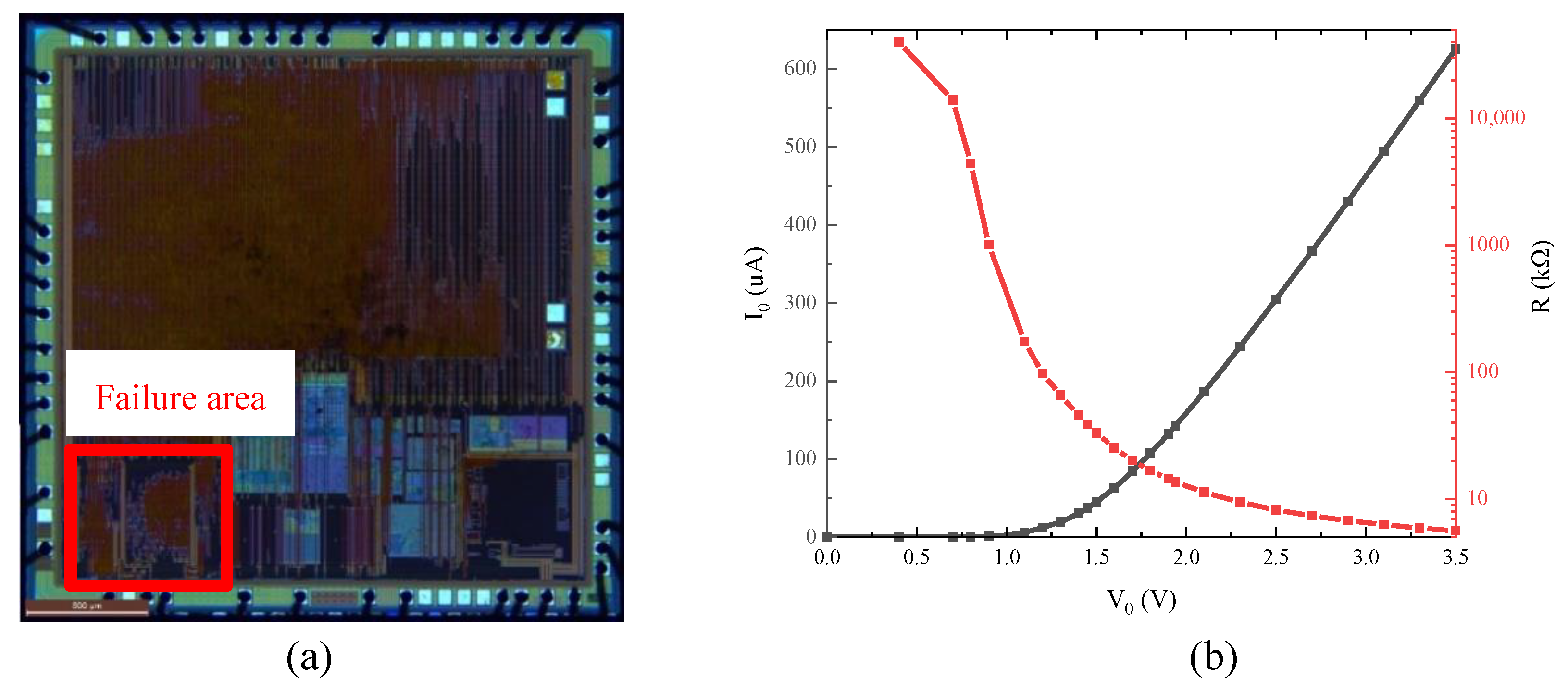
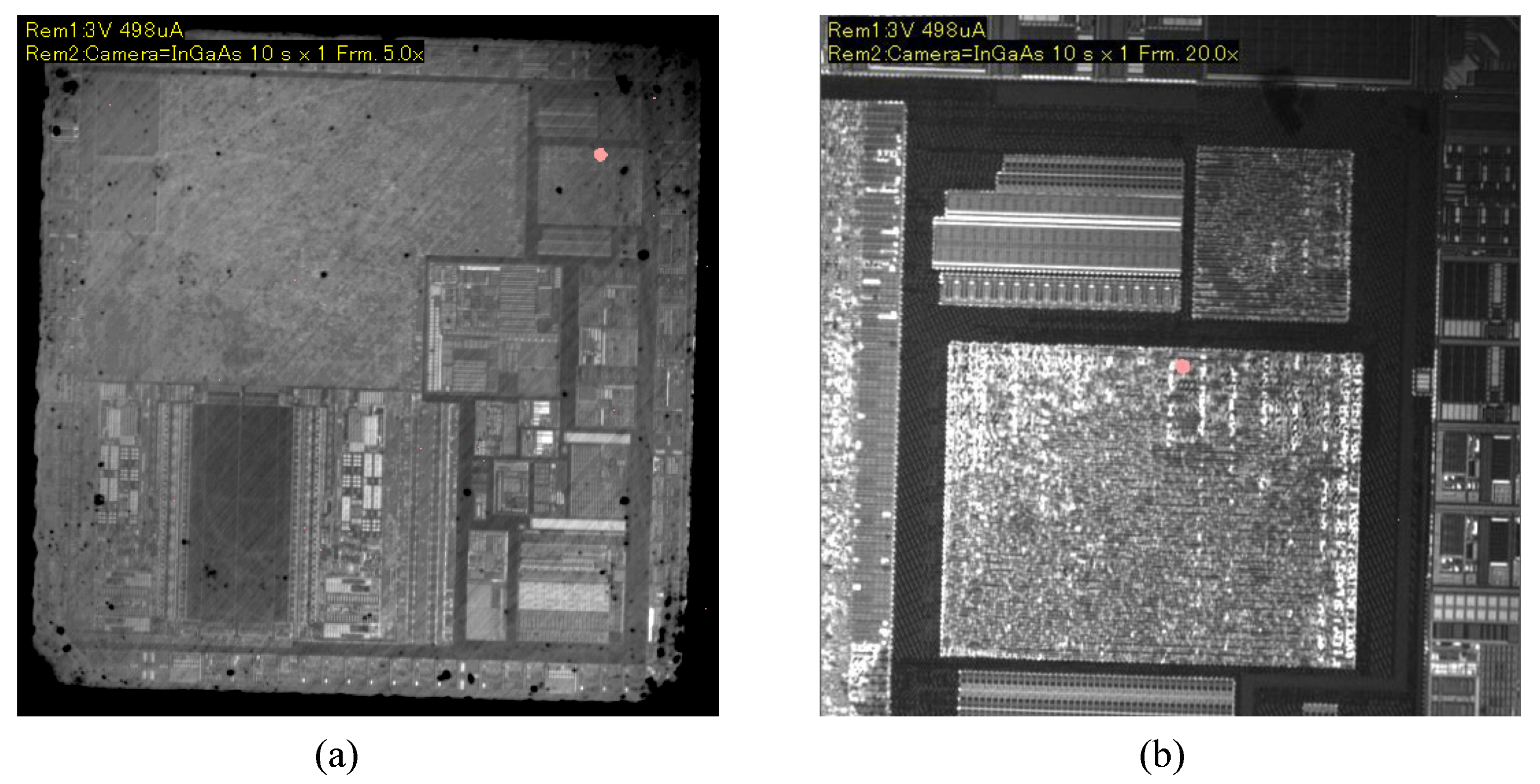
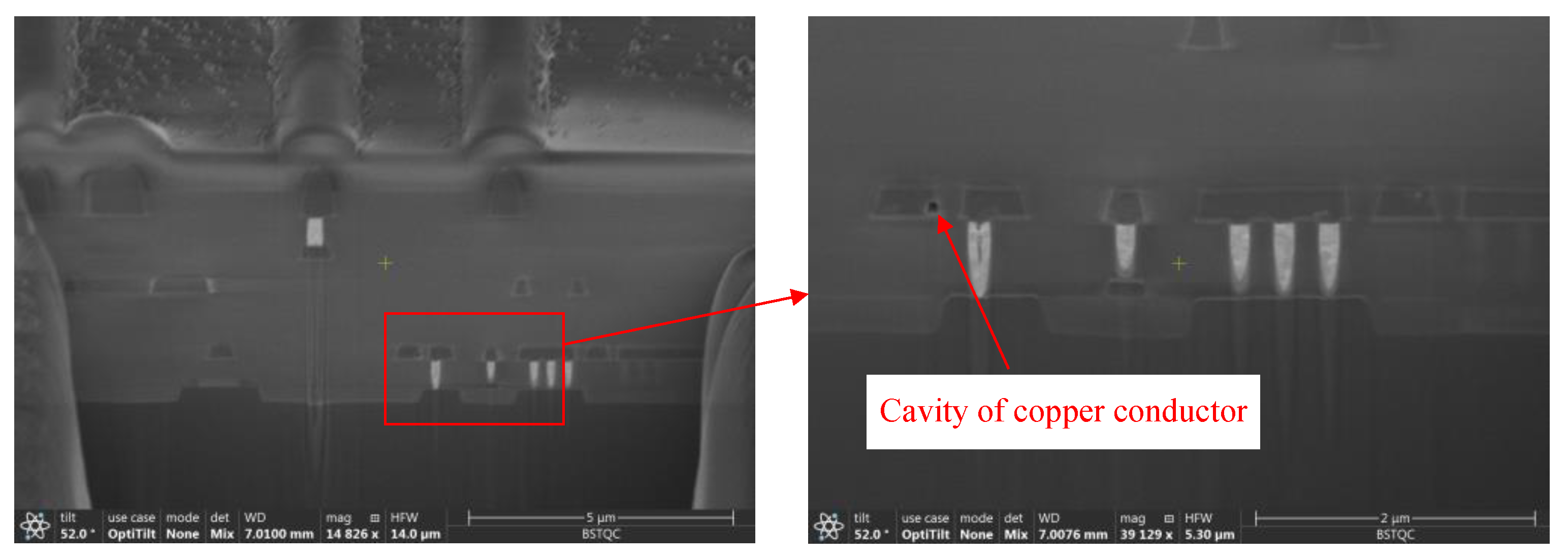
3.2.1. Failure Localization

When V 0 is set at 3.5 V, the current of the sample I 0 is 626 μA. According to the back-side CCD image (Figure 5a), the size of the sample is 2450 μm × 2450 μm. Set the lower-left corner of the chip as the origin of the coordinates, the horizontal direction as the X-axis, and the vertical direction as the Y-axis (Figure 5a). After laser-scanning with a 40 mW laser beam, the abnormal spot is determined, and the coordinates are ( X fail = 2064 μm, Y fail = 2033 μm) (Figure 5b). The abnormal current variation at the abnormal spot is about 2.5 μA, while the current variation at the normal spot is about 0.5 μA (Figure 5c). This result is in accordance with the result tested by Emission Microscopy (EMMI) (Figure 6), which is another common defect localization technology [18]. Figure 7 shows a possible physical reason for the failure, that is a cavity in the copper, found by the Focused Ion Beam (FIB) facility.

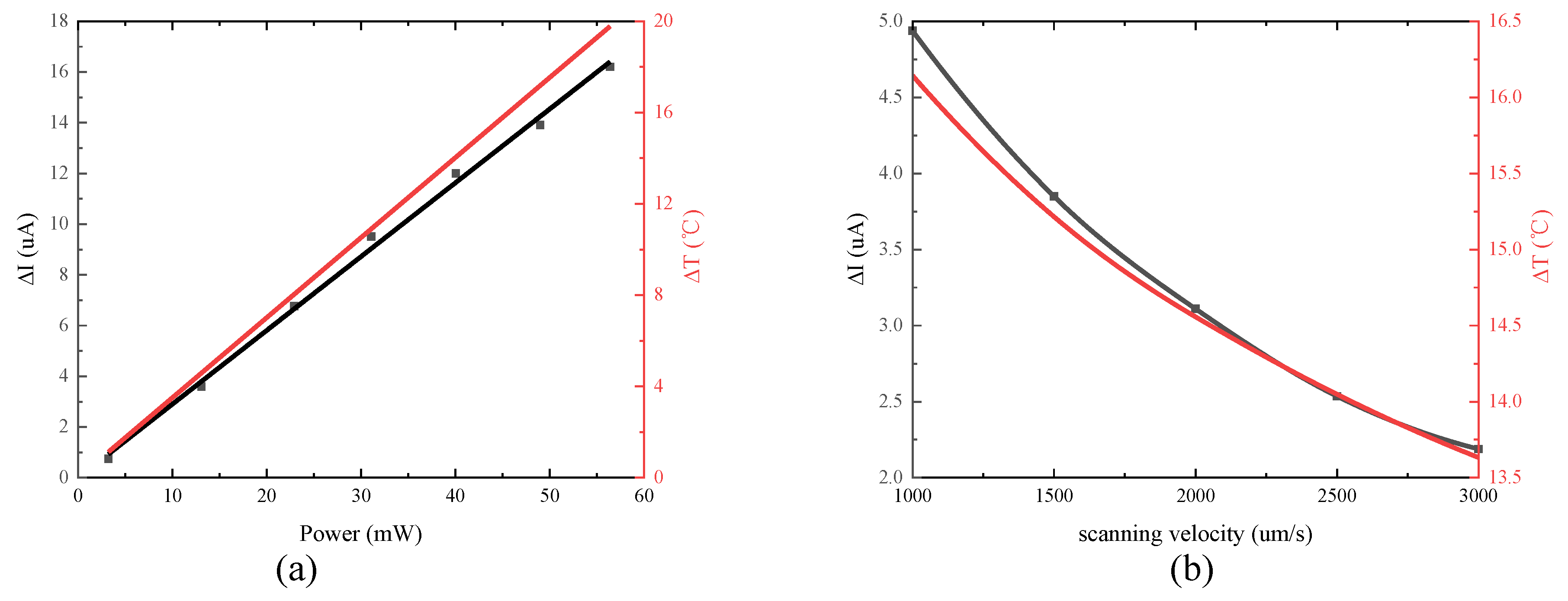
3.2.2. The Relationship between Current Variation and Laser Power and Scanning Velocity

Figure 8 shows the relationship between current variation and laser power and scanning velocity at the abnormal spot. A constant voltage bias set at 3.5 V is used. Figure 8 also shows the maximum Δ T during laser irradiation as a function of laser power and scanning velocity at ( x = 0 , y = 0 ) according to Equation (12). The experimental results meet these two conclusions based on the positive ratio of Δ T and Δ I .

3.2.3. Response Time for Laser Irradiation

As mentioned above, the evolution of the temperature field with time varies with different materials and structures. This can also be semi-quantitatively explained by the comprehensive model. As a comparison, Points A (abnormal spot) and B (normal spot, x A x B = 100 μm, y A y B = 0 μm) in Figure 9, are selected for laser irradiation testing. Several typical bias voltages are selected to test the response of the current variation (Figure 10a,b). The positive or negative value of the current variation will be discussed in Section 3.2.4.
Due to Equation (12), when the scanning velocity is zero, the temperature variation at the location ( x = 0 , y = 0 ) is:
Δ T ( 0 , t ) = 1 R P 0 4 π ρ c γ 0 t d t ω 2 + 4 k t t = 1 R P 0 16 π κ γ ln 1 + 4 k t ω 2
Although Equation (23) shows that the temperature always increases with laser irradiation time, the increase is very slow after a long time. This is consistent with the pattern shown in Figure 10. Besides, From Equation (20), the current variation is proportional to Δ T . The response time at the abnormal spot (less than 100 ms) is much less than that at the normal spot (more than 1 s). This is caused by the different materials and structures in the DUT. The material at the abnormal spot is metal Cu with extremely high thermal conductivity, so k = κ ρ c is relatively large. However, the material at the normal spot is the insulation material with low κ , causing the small k.
In addition, according to Equation (16), the OBIRCH technique dominates as Δ I > 0 , while the SEI dominates as Δ I < 0 . Therefore, the OBIRCH and SEI techniques have very similar response times from Figure 10. This conclusion is in accord with the predictions of the comprehensive model also because Δ I is proportional to Δ T .

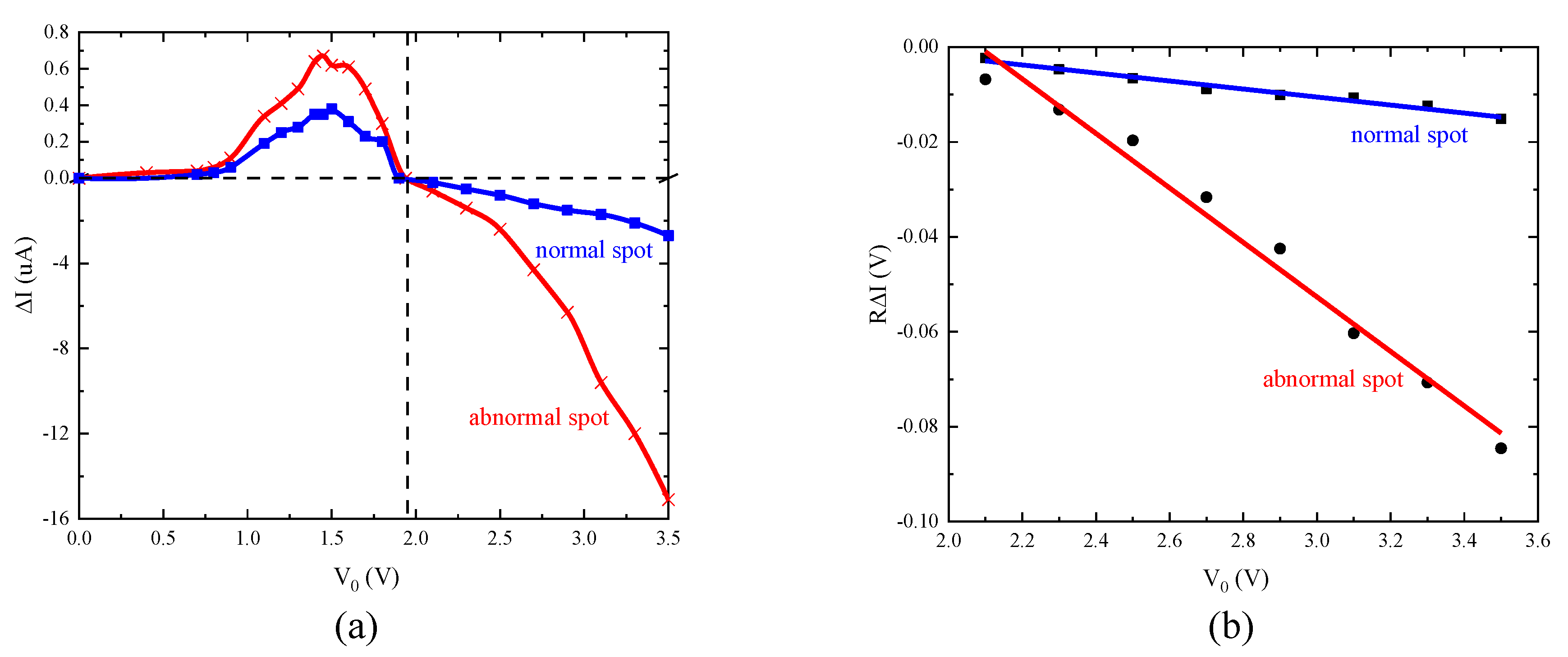
3.2.4. The Relationship between Current Variation and Voltage Bias

Adjusting the voltage bias conditions V 0 , Δ I will generate a series of complex changes (Figure 11a). As mentioned above, there exists a critical voltage V c = 1.94 V.
When V 0 is set between 1.8 V and 3.5 V, the OBIRCH technique dominates, and Δ I is negative. According to Equation (16), the contribution of OBIRCH, V 0 R 2 Δ R , is proportional to V 0 and inversely proportional to R 2 . Next, the resistance R decreases as the bias voltage V 0 increases (Figure 4b). Besides, Δ V S is invariable because the Seebeck voltage is only related to the temperature gradient T according to Equation (14). Δ R / R is also a constant because of the following formula:
Δ R R = ρ 0 α TCR Δ T A d l ρ 0 d l A = α TCR Δ T ¯
where Δ T ¯ is the average value of the temperature variation. Equation (13) is used in this formula. Therefore, the absolute value of Δ I ’s slope gradually increases as the V 0 increases. In order to find the values of Δ V S and Δ R / R , Equation (16) is modified to:
R Δ I Δ V S Δ R R V 0
The relationship between R Δ I and V 0 is shown in Figure 11b. After linear fitting, the values of Δ V S and Δ R / R are calculated and listed in Table 4. These two values at Point A are much larger than those at Point B, showing that the thermal property at the abnormal spot is more sensitive than that at the normal spot. Besides, the critical voltage V c can be calculated through Equation (17) using the data in Table 4, which is respectively 2.09 V at Point A and 1.75 V at Point B. These two values are close to the measured values V c = 1.94 V.
When V 0 is set between 0 V and 1.8 V, the SEI technique dominates, and Δ I is positive. Near 0 V (no bias applied), the resistance is so large that the value of Δ I tends to be zero. As the voltage increases, the resistance reduces, causing an increasing Δ I . In this period, OBIRCH’s contribution is still small. At about 1.5 V (Figure 11a), Δ I is most affected by the SEI. After that, Δ I starts to fall.
In general, although the comprehensive model has many shortcomings, such as the inability to describe the temperature variation in the z direction, the inability to describe the temperature field evolution with different structures of the IC, the infinite increase of the temperature when the scanning velocity is zero, etc., it fits well with the experimental results. An in-depth study on the optimization of the comprehensive model is under way.

4. Conclusions

A theoretical comprehensive model of the TLS technique is proposed. The model quantitatively explains the experimental results in TLS technology.
Firstly, it shows that after the laser irradiation, the temperature variation has a positive correlation with the laser power and a negative correlation with the scanning velocity. Since the current variation is proportional to the temperature variation, it also meets these correlations.
Secondly, the response curve of the current variation is similar to the temperature response curve. A high coefficient k = κ ρ c at the abnormal spot of the DUT leads to a faster response rate than that at the normal spot. Besides, the response times in the OBIRCH and SEI techniques are almost equal. Therefore, these two techniques can be switched simply by adjusting the voltage bias.
Finally, the resistivity variation and the Seebeck voltage are generated together with the temperature field. At constant voltage bias, these two effects have opposite contributions to the current variation. As voltage varies, the current variation Δ I can be positive or negative under the laser irradiation. To get more precise results in the testing process, a high voltage bias should be used in the OBIRCH technique. Similarly, a high current bias should be used in the TIVA technique. Conversely, the SEI technique requires a low bias condition.

Author Contributions

Conceptualization, Y.L. and H.W.; Formal analysis, H.Y.; Investigation, H.Y.; Methodology, H.Y.; Project administration, R.C.; Resources, Y.M.; Supervision, J.H.; Validation, Y.L.; Writing—original draft, H.Y.; Writing—review & editing, R.C. and J.H. All authors have read and agreed to the published version of the manuscript.

Funding

This project was supported by Beijing Municipal Commission of Science and Technology (Grant No. E039360101).

Conflicts of Interest

The authors declare no conflict of interest.

References

  1. Ross, R.J. Microelectronics Failure Analysis: Desk Reference, 6th ed.; ASM International: Materials Park, OH, USA, 2011. [Google Scholar]
  2. Herfurth, N.; Wu, C.; Beyreuther, A.; Nakamura, T.; De Wolf, I.; Simon-Najasek, M.; Altmann, F.; Croes, K.; Boit, C. Non-invasive soft breakdown localisation in low k dielectrics using photon emission microscopy and thermal laser stimulation. Microelectron. Reliab. 2019, 92, 73–78. [Google Scholar] [CrossRef]
  3. Lellouchi, D.; Lafontan, X.; Dhennin, J. MEMS Failure Analysis Case Studies Using the IR-OBIRCH Method-Short Circuit Localization in a MEMS. In Proceedings of the 2009 16th IEEE International Symposium on the Physical and Failure Analysis of Integrated Circuits, Suzhou, China, 6–10 July 2009. [Google Scholar]
  4. Lin, H.S.; Wu, M.S. A case study of high temperature pass analysis using thermal laser stimulation technique. In Proceedings of the 2010 IEEE International Reliability Physics Symposium, Garden Grove, CA, USA, 2–6 May 2010. [Google Scholar]
  5. Beaudoin, F.; Imbert, G.; Perdu, P.; Trocque, C. Current leakage fault localization using back-side OBIRCH. In Proceedings of the 2001 8th International Symposium on the Physical and Failure Analysis of Integrated Circuits, Singapore, 13 July 2001. [Google Scholar]
  6. Nordin, N.F. Application of Seebeck Effect Imaging on failure analysis of via defect. In Proceedings of the 2012 19th IEEE International Symposium on the Physical and Failure Analysis of Integrated Circuits, Singapore, 2–6 July 2012. [Google Scholar]
  7. Beaudoin, F.; Desplats, R.; Boit, C. Principles of Thermal Laser Stimulation Techniques. In Microelectronics Failure Analysis: Desk Reference; ASM International: Materials Park, OH, USA, 2004; pp. 417–425. [Google Scholar]
  8. Desplats, R.; Beaudoin, F.; Perdu, P.; Poirier, P.; Tremouilles, D.; Bafleur, M.; Lewis, D. Backside Localization of Current Leakage Faults Using Thermal Laser Stimulation. Microelectron. Reliab. 2001, 41, 1539–1544. [Google Scholar] [CrossRef]
  9. Jacobs, K.J.P.; Wang, T.; Stucchi, M.; Gonzalez, M.; Croes, K.; De Wolf, I.; Beyne, E. Lock-in thermal laser stimulation for non-destructive failure localization in 3-D devices. Microelectron. Reliab. 2017, 76, 188–193. [Google Scholar] [CrossRef]
  10. Nikawa, K.; Inoue, S. New Capabilities of OBIRCH Method for Fault Localization and Defect Detection. In Proceedings of the 6th Asian Test Symposium (ATS’97), Akita, Japan, 17–18 November 1997. [Google Scholar]
  11. Cole, E.I., Jr.; Tangyunyong, P.; Benson, D.A.; Barton, D.L. TIVA and SEI developments for enhanced front and back-side interconnection failure analysis. Microelectron. Reliab. 1999, 39, 991–996. [Google Scholar] [CrossRef]
  12. Beaudoin, F.; Chauffleur, X.; Fradin, J.P.; Perdu, P.; Desplats, R.; Lewis, D. Modeling Thermal Laser Stimulation. Microelectron. Reliab. 2001, 41, 1477–1482. [Google Scholar] [CrossRef]
  13. Brahma, S.K.; Boit, C.; Glowacki, A. Seebeck Effect Detection on Biased Device without OBIRCH Distortion Using FET Readout. Microelectron. Reliab. 2005, 45, 1487–1492. [Google Scholar] [CrossRef]
  14. Giowacki, A.; Boit, C. Characterization of thermoelectric devices in ICs as stimulated by a scanning laser beam. In Proceedings of the 2005 IEEE International Reliability Physics Symposium, San Jose, CA, USA, 17–21 April 2005. [Google Scholar]
  15. Sanchez, K.; Desplats, R.; Beaudoin, F.; Perdu, P.; Dudit, S.; Vallet, M.; Lewis, D. Dynamic Thermal Laser Stimulation Theory and Applications. In Proceedings of the 2006 IEEE International Reliability Physics Symposium Proceedings, San Jose, CA, USA, 26–30 March 2006. [Google Scholar]
  16. Bray, J.W. Metals Handbook, vol 2: Properties and Selection: Nonferrous Alloys and Special-Purpose Materials, 10th ed.; ASM International: Materials Park, OH, USA, 1990. [Google Scholar]
  17. Dizaji, A.F.; Jafari, A. Three-dimensional fundamental solution of wave propagation and transient heat transfer in non-homogenous media. Eng. Anal. Bound. Elem. 2009, 33, 1193–1200. [Google Scholar] [CrossRef]
  18. Naoe, T.; Mizobe, T.; Yokoyama, K. Case studies of defect localization based on software based fault diagnosis in comparison with PEMSOBIRCH analysis. Microelectron. Reliab. 2014, 54, 1433–1442. [Google Scholar] [CrossRef]
Figure 1. Seebeck effect principle. A Seebeck voltage is generated due to the temperature difference of the two contiguous materials.
Applsci 10 08576 g001
Figure 2. Laser beam focused on the metal layer. The thermal energy will diffuse in all directions.
Applsci 10 08576 g002
Figure 3. Schematic diagram of the Laser Scanning and Testing System (LSTS). The voltage source is used to supply the DUT, and the computer is used to monitor the current. As the laser beam scans the defect location, the abnormal Δ I will be tested, and a red spot will be marked on the layout diagram, which is imaged by the IR-CCD.
Applsci 10 08576 g003
Figure 4. Characteristics of the failed sample: (a) front-side optical image of the MCU sample and the location of the failure area; (b) I-V and R-V curves.
Applsci 10 08576 g004
Figure 5. Localization of the abnormal spot using the LSTS: (a) The back-side CCD image of the DUT. The scanning scheme is shown by the white line and arrow. (b) While the laser is scanning the abnormal spot, an abnormal current is tested by the current meter, and a red spot is marked on the failure spot. (c) The abnormal current variation is about 2.5 μA, while the normal current variation is about 0.5 μA.
Applsci 10 08576 g005
Figure 6. Defect localization by Emission Microscopy (EMMI). The voltage is set at 3 V. An InGaAs IR-camera is used for imaging: (a) the magnification is 5.0×; (b) the magnification is 20.0×.
Applsci 10 08576 g006
Figure 7. Cavity of the copper conductor found by the Focused Ion Beam (FIB), which is probably the physical cause of the failure.
Applsci 10 08576 g007
Figure 8. Comparison of the current variation Δ I in the experiment and temperature variation Δ T in the comprehensive model. Δ T is calculated through Equation (12) using the data in [16]. (a) The laser power varies while the scanning velocity is set at 2500 μm/s. (b) The scanning velocity varies while the laser power is set at 40 mW.
Applsci 10 08576 g008
Figure 9. Two selected spots for laser irradiation testing. The laser will continuously irradiate Point A or Point B.
Applsci 10 08576 g009
Figure 10. Curve of the current variation and the irradiation time at different bias voltages V 0 . The laser beam starts to irradiate at t = 10 s with no scanning velocity. The laser power is set at 40 mW: (a) Point A (abnormal spot); (b) Point B (normal spot).
Applsci 10 08576 g010
Figure 11. Curve of the current variation and the bias voltage: (a) Δ I V 0 ; (b) R Δ I V 0 .
Applsci 10 08576 g011
Table 1. Resistivity and temperature coefficients of some metal materials [16].
Material ρ 0 (20 °C) ( Ω · m ) α TCR (°C−1)
Al 2.9 × 10 8 4.3 × 10 3
Cu 1.7 × 10 8 3.9 × 10 3
Table 2. Seebeck coefficients for several materials and junctions [16].
Material or Junction S 1 2 ( μ V / K )
Al−3.5 *
W3.6 *
Al/n + Si287 **
Al/p + Si−202 **
* Measured relative to copper, ** relative thermoelectric power for a 10 18 cm−3 doping.
Table 3. Relevant parameters of the LSTS.
laserWavelength1310 nm
Power0∼100 mW
Translation StageScanning Speed0∼100 mm/s
Positioning Accuracy0.1 μm
Table 4. Values of Δ V S and Δ R / R .
Δ V S Δ R / R
Point A (abnormal spot)0.1200.0574
Point B (normal spot)0.01480.00845
Publisher’s Note: MDPI stays neutral with regard to jurisdictional claims in published maps and institutional affiliations.

