Featured Application
A fully integrated power inductor using a silicon interposer is proposed, which is appropriate for miniaturized power management applications.
Abstract
Inductor integration is of vital importance for miniaturization of power supply on chips. In this paper, a backside integrated power inductor is presented. The inductor is placed at the backside of a silicon interposer and connected to the front side metal layers by through-silicon vias (TSVs) for area saving and simple fabrication. An inductance model is proposed to effectively capture the total inductance of the power inductor by an analytical method. The results obtained from the analytical model and finite element method exhibit good agreement with various design parameters and the error between the proposed model and measurement remains less than 7.91%, which indicates that the proposed model can predict the inductance suitably.
1. Introduction
An inductor is a fundamental component for electronic devices, which is used for energy storage and filtering, but it dominates in size and loss. To achieve its miniaturization and aid lowering the cost of the power supply on chip, monolithic integration of power inductors is essential [1,2,3,4]. Lots of design methodologies and fabrication technologies have been proposed for potential monolithic integration.
The increase in switching frequencies of power circuits up to megahertz can significantly reduce the inductor’s size [5,6]. A tiny 0.47 μH inductor has been used in a commercial 8 MHz PWM synchronous Buck regulator [5]. A 250 MHz buck regulator has been implemented with a 12 nH wire-bond power inductor in [6]. However, such a high frequency will cause high power switching and result in poor efficiency (e.g., 71% [6]). Furthermore, the power inductor with low inductance easily introduces a high ripple current. Various magnetic core materials have been adopted to enhance the inductance density for monolithic integration of power inductors [7,8,9]. A 3D in-silicon magnetic core toroidal inductor is presented in [7], in which the magnetic powder-based core is embedded into an air-core inductor using a casting method. A 3D solenoid inductor that is embedded in the substrate and integrated an iron core is reported in [8]. However, the introduction of magnetic material not only causes a core saturation issue but also increases the design and fabrication complexity.
In this paper, a fully integrated air-core power inductor is proposed, which is developed for a high-density silicon-interposer based on 2.5D and 3D integrated circuits, and a compact analytical model has been derived to capture the total inductance of the proposed inductor, where the screw pitch and cross-sectional sharp are considered. Comparted to traditional circular coil method [10,11] and the model developed for coils with a circular section-area [12], the proposed model can offer a better accuracy and is more suitable for the inductance prediction of power inductance fabricated with 2D planar technology.
2. Inductance Model Description
Figure 1a shows the cross-section schematic of a silicon-interposer-based 3D IC package, in which the interposer acts as bridges between the active chips and printed circuit board package [13,14]. In addition to the interconnection, the interposer provides the functionalities with passive components integration. Various integrated passive devices, such as TSV inductors, TSV capacitors and TSV filters, have been presented [15,16,17]. However, these studies focus on the utilization of tiny TSVs. The TSV-based solenoid inductor has a low inductance and is not suitable for power device applications. In this design, a fully integrated power inductor is proposed, as shown in Figure 1. The proposed inductor is designed to be placed at the backside of the interposer for efficiently utilizing the silicon area and can be connected to the front side power circuits through TSVs. A thin oxide dielectric is inserted between the inductor and silicon substrate to obtain a high-quality factor.
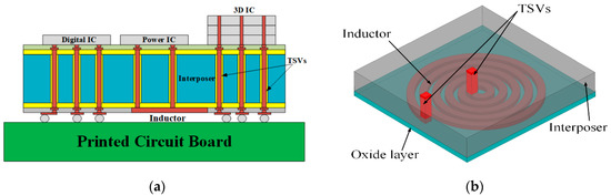
Figure 1.
Schematic of (a) the 3D IC package and (b) the 3D view of the proposed backside integrated power inductor.
Figure 2 shows the major fabrication steps of the proposed power inductors. Firstly, the via structure is formed at the front side of the interposer by deep reactive ion etching (Figure 2a). The etched via is then processed with an oxide dielectric, a Ta barrier and a Cu seed layer, followed by the acid Cu electroplating (Figure 2b). The Cu damascene technique [18] is adopted to fabricate the redistribution layers (RDLs) and the vias connecting the TSVs to the RDLs (Figure 2c). The topside of the interposer wafer is temporarily bonded to a carrier by adhesive and a back grinding is carried out to a few microns to the TSVs (Figure 2d). The proposed inductor is implemented by the RDLs at the backside with the Cu damascene method and the vias connecting the TSVs and the inductor are completed (Figure 2e). Finally, one de-bonds the carrier wafer and assembles the TSV module on the package substrate (Figure 2f).
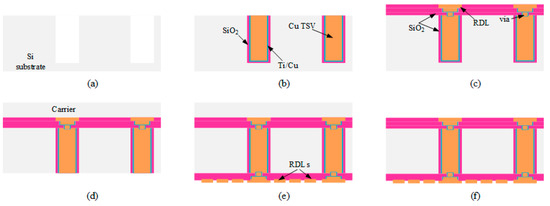
Figure 2.
Schematic of the major fabrication steps:(a) via formation, (b) via filling, (c) RDLs and vias formation, (d) Temporary bonding and backside grinding, (e) inductor formation, (f) TSV module assemble.
With the help of the finite-element method simulation with HFSS software, the electrical performance of the proposed backside integrated inductor with a size of 1 mm2 is investigated. Table 1 provides a performance comparison for the proposed backside integrated inductor with other state-of-the-art works. Where L, Q, f and RDC are the inductor inductance, qualify factor, switching frequency and dc resistance, respectively; η is the inductor efficiency, which is estimated by the inductor parameters and the equation in [19,20] for power efficiency. Since the oxide dielectric provides a good isolation between the inductor and the silicon substrate, it is observed that the proposed inductor achieves a higher qualify factor, leading to a peak inductor efficiency of 87.3% for a typical voltage conversion ratio of 1.8 V:0.9 V and load current of 100 mA. On the contrary, substrate loss and eddy current loss significantly decrease the quality and efficiency of the silicon-core inductors and magnetic-core inductors. Furthermore, in comparison to the toroidal inductor, the proposed embedded inductor is more compatible with the standard CMOS process.

Table 1.
Comparison of the proposed backside integrated inductor with the prior integrated power inductors.
Based on the above structure, the resistance–inductance–capacitance (RLC) model of the backside integrated inductor can be established. Considering that the inductance is one of the critical parameters for inductors in power management applications, this work focuses on the modeling and analysis of the inductance of the proposed inductor. For the basis analysis, it is assumed that the track width is w, the track spacing is s and the track thickness is t. The linked flux of the inductor determined its inductance. For a one-turn inductor, the overall inductance of the inductor is equal to its self-inductance. For multi-turn inductors, there is mutual coupling between each turn, and then the magnetic field strength through the inductor and the linked flux significantly increases with the number of turns, as shown in Figure 3. Therefore, the overall inductance of the inductor is the sum of the self-inductance and increased mutual inductance between each turn [22]. For the proposed Archimedean spiral coil with a rectangular cross section area and n concentric turns, the total inductance LT can be written as the sum over the self-inductance LS and the mutual inductance LM of all turns,
where Mij represent the mutual inductance between the ith turn coil and jth turn coil. The overall self-inductance LS can be further approximated as a function of coil geometry [23],
where leng is the total length of the n-turn coil, and μ = 4π × 10−7 H/m is the permittivity of the surrounding medium. For an Archimedean spiral coil with an inner radius R0 and screw pitch p (p = w + s), leng can be calculated by
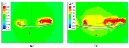
Figure 3.
Magnetic field strength in (a) a one-turn coil and (b) a two-turn coil.
The mutual inductance Mij can be calculated using the classical magnetic vector potential approach as [22,24,25,26]
For an Archimedean spiral coil, the tangent vector of point P (Ricosθ1, Risinθ1, 0) on the ith coil and point Q (Rjcosθ2, Rjsinθ2, 0) on the jth coil can be derived as
and then
The distance between two points P and Q can be expressed as
Substituting Equation (5)–Equation (7) into Equation (4), Mij can be obtained as
Substituting Equations (3) and (8) into Equation (1), the total inductance of the proposed Archimedean coil can be calculated.
3. Validation and Discussion
In this section, the inductances obtained from the proposed model, the traditional circular coil method (CCM), quasi-static electromagnetic simulation with Q3D, are compared [26]. Q3D is a fast-quasi-static electromagnetic field simulator and is good at RLCG parameter extraction. For the proposed power inductor with the inductance of ~1 μH, its switching frequency would not exceed 100 MHz. Therefore, Q3D can provide an accurate inductance extraction for the proposed power inductor. In the simulation environment, the two terminals of the inductor are defined as a source and sink, respectively, and the AC RL solver are adopted for inductance extraction. In the circular coil method [10,11], each loop is approximated as a circle and the radius of the ith turn is treated as R0 + (i−1)p. The base parameters are w = 40 μm, t = 20 μm, s = 20 μm, R0 = 20 μm and n = 26. As shown in Figure 4, the inductances with the proposed model agree well with the results of 3D simulators over various design parameters: the error with respect to the EM results is less than 9.5%, while the error of the traditional circular coil method is 40.2%. The comparison indicates that the proposed model can be used for inductance extraction of the fully integrated power inductor.
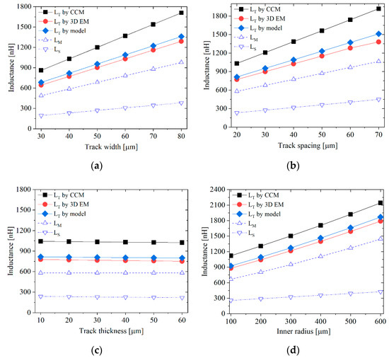
Figure 4.
Impact of (a) track width, (b) track spacing, (c) track thickness and (d) inner radius on the total inductance.
Furthermore, the results in Figure 4a,b demonstrate that LT increases with the track width w and track spacing s, due to the increased partial self-inductance and mutual inductance according to Equations (2) and (8). Since the variation in partial self-inductance and mutual inductance with track thickness t is little, it can be seen in Figure 4c that the impact of the parameter on LT can be negligible. Moreover, the results in Figure 4d show the overall inductance would increase with the inner radius of the inductor.
Table 2 investigates the computational efficiency of the model by comparing the simulation time of the proposed analytical model and 3D EM simulator using the parameters listed. The simulation was performed on an Intel i5 core with a processor speed of 3.0 GHz and 8 GB of RAM. It was found that lots of computational time can be saved using the proposed model.
Table 2.
Comparison of computational efficiency.
To verify the accuracy of the analytical expressions, the proposed model was applied to the fabricated power inductors. Taking into account the additional process steps for the 3D integration and the weak impact of the interposer materials on the inductor’s performance, the proposed power inductor was fabricated with 2-layer Print Circuit Board (PCB) technology. In the emulated 3D integration environment shown in Figure 5a, the inductor is realized on the backside planar track. The vias in the PCB technology imitate the TSVs to connect the inductor to the frontside power circuits. Table 3 compares the inductances obtained from this model, the circular coil method (CCM) [10,11] and electrical measurement with a Hioko IM3570 Impedance Analyzer. By connecting the two terminals of the inductor to the two probes of the impedance analyzer, capable of measurement frequencies of 4 Hz to 5 MHz, the inductance at 1 MHz can be captured. It is observed that the proposed model shows a higher accuracy in comparison to CCM. The maximum error and average error of the proposed model are 7.91% and 3.72%, respectively, which indicates the feasibility of the proposed model for inductance prediction.
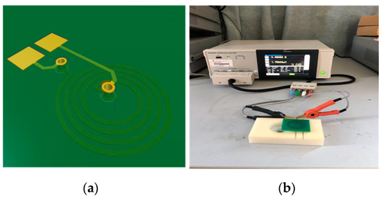
Figure 5.
(a) Schematic view of the fabricated power inductor and (b) its experimental setup.
Table 3.
Comparison of the inductance results.
4. Conclusions
In this paper, a power inductor integration technology for 2.5D/3D integrated power management applications is presented and experimentally demonstrated. The inductor can be integrated at the backside of the silicon interposer and interconnects with the frontside power circuits with TSVs. A compact and accurate inductance model is developed to capture the overall inductance of the proposed inductor. A comparison with 3D EM results shows that the proposed analytical model has a good prediction capability and a high computational efficiency. Furthermore, the model results show that the increase in track width, track spacing and inner radius of the inductor would increase the overall inductance, while the variation in the inductance with track thickness is less. Finally, the inductance from the proposed model and the measurements were compared, and an error of less than 7.91% was obtained.
Author Contributions
Conceptualization, K.Q.; methodology, K.Q.; validation, K.Q and L.Q.; formal analysis, K.Q and L.Q.; investigation, K.Q.; resources, K.Q.; data curation, K.Q.; writing—original draft preparation, K.Q.; writing—review and editing, K.Q and L.Q.; supervision, L.Q.; project administration, L.Q.; funding acquisition, L.Q. All authors have read and agreed to the published version of the manuscript.
Funding
This work was supported by the National Natural Science Foundation of China under Grants 61771268, U1709218 and the K.C. Wong Magna Fund in Ningbo University.
Conflicts of Interest
The authors declare no conflict of interest.
References
- Li, Y.; Zhu, Z. A 30W 90% efficiency dual mode-controlled DC-DC controller with power over ethernet interface for power device. IEEE Trans. Very-Large Scale Integr. Syst. 2017, 25, 1943–1950. [Google Scholar] [CrossRef]
- Vaisband, I.; Friedman, E.G. Heterogeneous methodology for energy efficient distribution of on chip power supplies. IEEE Trans. Power Electron. 2013, 28, 4267–4274. [Google Scholar] [CrossRef]
- Fletcher, B.; Das, S.; Mak, T. Design and optimization of inductive coupling links for 3-D ICs. IEEE Trans. Very-Large Scale Integr. Syst. 2019, 27, 711–722. [Google Scholar] [CrossRef]
- Zeng, J.; Wang, C.; Sangster, A. Theoretical and experimental studies of flip-chip assembled high Q suspended MEMs inductors. IEEE Trans. Microw. Theory Tech. 2017, 55, 1171–1180. [Google Scholar] [CrossRef]
- Shepard, J. Micrel’s MIC2285 merges LDO and buck regulator. New Ind. Prod. 2006. Available online: https://eepower.com/new-industry-products/micrels-mic2285-merges-ldo-and-buck-regulators/ (accessed on 27 September 2020).
- Kar, M.; Singh, A.; Rajan, A.; De, V.; Mukhopadhyay, S. An all-digital fully integrated inductive buck regulator with a 250MHz multi-sampled compensator and a lightweight auto-tuner in 130nm CMOS. IEEE J. Solid-State Circuits 2017, 52, 1825–1832. [Google Scholar] [CrossRef]
- Le, H.; Nour, Y.; Pavlovic, Z.; Mathuna, C.; Knott, A.; Jensen, F.; Han, A.; Ouyang, Z. High-Q 3D micro fabricated magnetic-core toroidal inductors for power supplies in package. IEEE Trans. Power Electron. 2019, 34, 74–77. [Google Scholar] [CrossRef]
- Xu, T.; Sun, J.; Wu, H.; Li, H.; Tao, Z. 3D MEMS in chip solenoid inductor with high inductance density for power MEMS device. IEEE Electron. Device Lett. 2019, 40, 1816–1820. [Google Scholar] [CrossRef]
- Jia, H.; Lu, J.; Wang, X.; Padmanabhan, K.; Shen, Z. Integration of a monolithic buck converter power IC and bond wire inductors with ferrite epoxy glob cores. IEEE Trans. Power Electron. 2011, 26, 1627–1633. [Google Scholar] [CrossRef]
- RamRakhyani, A.; Mirabbasi, S.; Chiao, M. Design and optimization of resonance based efficient wireless power delivery systems for biomedical implants. IEEE Trans. Biomed. Circuits Syst. 2011, 5, 48–59. [Google Scholar] [CrossRef]
- Kim, D.; Kim, J.; Park, Y. Optimization and design of small circular coils in a magnetically coupled wireless power transfer system in the megahertz frequency. IEEE Trans. Microw. Theory Technol. 2016, 64, 2652–2664. [Google Scholar] [CrossRef]
- Khan, S.R.; Pavuluri, S.K.; Desmulliez, M.P.Y. Accurate modeling of coil inductance for near-field wireless power transfer. IEEE Trans. Microw. Technol. Technol. 2018, 66, 4158–4168. [Google Scholar] [CrossRef]
- Sukumaran, V.; Bandyopadhyay, T.; Sundaram, V.; Tummala, R. Low cost thin glass interposers as a superior alternative to silicon and organic interposers for packaging of 3D ICs. IEEE Trans. Compon. Packag. Manuf. Technol. 2012, 2, 1426–1433. [Google Scholar] [CrossRef]
- Song, J.; Park, S.; Kim, S.; Kim, J.J.; Kim, J. Active silicon interposer design for interposer-level wireless power transfer technology for high density 2.5D and 3D ICs. IEEE Trans. Compon. Packag. Manuf. Technol. 2016, 6, 1148–1159. [Google Scholar] [CrossRef]
- Wang, F.; Yu, N. Simple and accurate inductance model of 3D inductor based on TSV. Electron. Lett. 2016, 52, 1815–1817. [Google Scholar] [CrossRef]
- Chang, Y.; Ko, C.; Yu, T.; Hsieh, Y.; Chen, K. Modeling and characterization of TSV capacitor and stable low capacitance implementation for wide I/O application. IEEE Trans. Device Mater. Reliab. 2015, 15, 129–139. [Google Scholar] [CrossRef]
- Yin, X.; Zhu, Z.; Liu, Y.; Liu, X.; Yang, Y. Ultra-compact TSV based L-C low-pass filter with stopband up to 40GHz for microwave application. IEEE Trans. Microw. Theory Tech. 2019, 2, 738–740. [Google Scholar] [CrossRef]
- Lau, J.; Tzeng, P.; Lee, C.; Zhan, C.; Li, M.; Cline, J.; Saito, K.; Kao, M. Redistribution layers (RDLs) for 2.5D/3D IC integration. J. Microelectron. Electron. Packag. 2014, 11, 16–24. [Google Scholar] [CrossRef]
- Wu, R.; Sin, J. A novel silicon-embedded coreless inductor for high-frequency power management applications. IEEE Electron. Device Lett. 2011, 32, 60–62. [Google Scholar] [CrossRef]
- Ding, Y.; Fang, X.; Wu, R.; Sin, J. A new fan-out package embedded power inductor technology. IEEE Trans. Electron. Devices 2020, 41, 268–271. [Google Scholar] [CrossRef]
- Le, H.; Nour, Y.; Han, A.; Jensen, F.; Ouyang, Z.; Knott, A. Microfabricated air-core toroidal inductor in very high frequency power converter. IEEE J. Emerg. Sel. Top. Power Electron. 2018, 6, 604–613. [Google Scholar] [CrossRef]
- Grover, F.W. Inductance Calculation: Working Formulas and Tables; Special Edition Prepared for Instrument Society America Press; Courier Corporation: New York, NY, USA, 1946. [Google Scholar]
- Yue, C.P.; Wong, S.S. Physical modeling of spiral inductors on silicon. IEEE Trans. Electron. Devices 2000, 47, 560–572. [Google Scholar] [CrossRef]
- Qian, L.; Chen, M.; Cui, K.; Shi, G.; Xia, Y. Modeling of mutual inductance between two misalignment planar coils in wireless power transfer. IEEE Microw. Wirel. Compon. Lett. 2020, 30, 814–817. [Google Scholar] [CrossRef]
- Qu, C.; Liu, Y.; Liu, X.; Zhu, Z. Inductance modeling of interconnects in 3-D stacked chip packaging. IEEE Microw. Wirel. Compon. Lett. 2018, 28, 281–284. [Google Scholar] [CrossRef]
- Manual of Ansoft Q3D. 2013. Available online: http://www.peraglobal.com/content/details_254_3020.html (accessed on 27 September 2020).
Publisher’s Note: MDPI stays neutral with regard to jurisdictional claims in published maps and institutional affiliations. |
© 2020 by the authors. Licensee MDPI, Basel, Switzerland. This article is an open access article distributed under the terms and conditions of the Creative Commons Attribution (CC BY) license (http://creativecommons.org/licenses/by/4.0/).