Article

Selective Plasma Etching of Polymer-Metal Mesh Foil in Large-Area Hydrogen Atmospheric Pressure Plasma

Department of Physical Electronics, CEPLANT—R&D Center for Plasma and Nanotechnology Surface Modifications, Faculty of Science, Masaryk University, Kotlářská 267/2, 61137 Brno, Czech Republic
*
Author to whom correspondence should be addressed.
Appl. Sci. 2020, 10(20), 7356; https://doi.org/10.3390/app10207356
Submission received: 29 September 2020 / Revised: 18 October 2020 / Accepted: 19 October 2020 / Published: 21 October 2020
(This article belongs to the Special Issue Plasma: From Materials to Emerging Technologies)

Abstract

:

Featured Application

Surface selective etching of polymer substrates, metal-polymer composites, e.g., transparent conductive substrates by atmospheric plasma roll-to-roll processing.

Abstract

We present a novel method of surface processing of complex polymer-metal composite substrates. Atmospheric-pressure plasma etching in pure H2, N2, H2/N2 and air plasmas was used to fabricate flexible transparent composite poly(methyl methacrylate) (PMMA)-based polymer film/Ag-coated Cu metal wire mesh substrates with conductive connection sites by the selective removal of the thin (~10–100 nm) surface PMMA layer. To mimic large-area roll-to-roll processing, we used an advanced alumina-based concavely curved electrode generating a thin and high-power density cold plasma layer by the diffuse coplanar surface barrier discharge. A short 1 s exposure to pure hydrogen plasma, led to successful highly-selective etching of the surface PMMA film without any destruction of the Ag-coated Cu metal wires embedded in the PMMA polymer. On the other hand, the use of ambient air, pure nitrogen and H2/N2 plasmas resulted in undesired degradation both of the polymer and the metal wires surfaces. Since it was found that the etching efficiency strongly depends on the process parameters, such as treatment time and the distance from the electrode surface, we studied the effect and performance of these parameters.

Graphical Abstract

1. Introduction

Plasma technologies using a wide scale of plasma working gases has succeeded as a powerful tool for surface cleaning, functionalization, adhesion improvement, deposition, sputtering and etching. Hydrogen plasma is a very strong reducing agent already tested for the surface treatments of metals, silicon, carbon, and polymer materials. A comprehensive summary of plasma etching of polymers and polymeric materials including the hydrogen plasma etching can be found in the review of Puliyalil and Cvelbar [1]. In general, when polymer surfaces are exposed to the hydrogen plasma, the bombardment by plasma species (electrons, hydrogen ions and radicals) led to the degradation of the surface and etching reactions will occur.
The effect of hydrogen content in low-pressure N2/H2 plasma for surface modification of polyethylene (PE), poly(tetrafluoroethylene) (PTFE) and polyvinylidene fluoride (PVDF) studied Sara-Bournet et al. [2]. Hydrogen-containing plasma was found to causing dehydrohalogenation along the fluoropolymer backbone [3]. Subsequently, the co-process gas can covalently attach to these sites; thus, the hydrogen plasma with a co-process gas can particularly improve the adhesive bonds of fluoropolymers. Selective removal of polymeric PMMA residues on monolayer graphene by high-density, low pressure H2 and H2/N2 plasmas without a damage to the graphene surface as examined by Cunge et al. [4]. Selective etching of graphene edges and graphene nanoribbons using hydrogen plasma reaction at 300 °C and at a pressure of 300 mTorr was studied by Xie et al. [5]. The advantage of selective plasma etching using hydrogen as etchant gas was used for selective preparation of metallic and semiconducting single-wall carbon nanotubes by Hou et al. [6] and Zhang et al. [7].
Inline plasma surface treatments showed a significant potential for applications in high volume and cost-effective roll-to-roll (R2R) fabrication of flexible electronics on a polymer web substrate including, for example, flexible solar cell and wearable electronics fabrication. Virtually all these applications need diffuse non-thermal plasma. We use the wording “diffuse plasma” in accordance with the term published for the first time by Šimor et al. in 2002 [8]. The “diffusivity” of the plasma is related to the visual uniformity of the generated plasma as observed by the human eye. So that we used the term diffuse plasma to refer to the plasma which, when visually observed, is widely spread, and not concentrated to individual plasma filaments. In our experience, the diffuse, visually uniform plasma enables uniform plasma surface modification working at the plasma exposure times longer than the time resolution of a human eye.
However, such plasma generated at low pressure in costly vacuum systems is at odds with high throughput processing required in industry [9]. However, the developments in the field of plasma physics during the last two decades have opened a way how to generate stable, diffuse and non-thermal plasma at atmospheric pressure [10]. The research of atmospheric plasma, including the atmospheric-pressure H2 plasma, has been driven by the need of replacing of expensive vacuum systems by simpler, more cost-effective and high-throughput systems [9]. For example, [11] studied plasma etching of various polymers like PP, PET, PEN, PEEK, PMMA, PLA, LDPE and Nylon 6.6 using atmospheric pressure hydrogen plasma. Kwon et al. [12] used hydrogen plasma sintering process at temperature 150 °C for reduction and densification of copper complex ink on flexible PET substrate.
The so-called Diffuse Coplanar Surface Barrier Discharge (DCSBD) is capable to generate visually an almost uniform diffuse ambient air plasma with effective thickness of approximately 0.25 mm [13]. Large-area atmospheric-pressure hydrogen plasma generated by DCSBDs in a geometry mimicking R2R treatment was studied for fast plasma reduction of graphene oxide film on flexible PET substrate [14]. It was also reported that DCSBD hydrogen plasma can be used for chemical reduction of a native surface CuO/CuO2 layers [15] as well as for etching of thin SiO2/Si films [16] and reduction of diamond nanoparticles [17]. Reducing DCSBD plasma was already used for surface modification [18] and nanostructuring of PMMA, PET and PTFE polymeric substrates [19].
In this paper hydrogen atmospheric pressure plasma generated by a DCSBD with the electrode geometry applicable for the R2R processing was used for etching of thin surface PMMA polymer layer from the top of polymer-metal mesh substrate used as a flexible transparent conductive substrate. The etching was studied by scanning electron microscopy (SEM) and using a laser confocal microscope. A chemical reduction of plasma-modified surfaces was analyzed by energy dispersive x-ray analysis (EDX). The effect of process parameters on the properties of etched surface was investigated too. The selectivity of plasma etching was studied through the etching in mixtures of nitrogen and hydrogen. DCSBD can generate atmospheric plasma in all technically important gases, such as ambient air, nitrogen and hydrogen. Since the use of pure atmospheric pressure hydrogen can be of some safety concern, we also tested the etching capability and selectivity of some other technically and economically helpful plasma gases.
The novelty of this work is that the reducing, large-area hydrogen plasma generated at atmospheric pressure was applied to a polymer-metal mesh substrate in order to carry out selective plasma etching together with the optimization of etching parameters, in particular: plasma-substrate distance, etching time and working gas specification. The selectivity of plasma etching is of great importance especially in case of processing of complex polymer-metal composite materials.

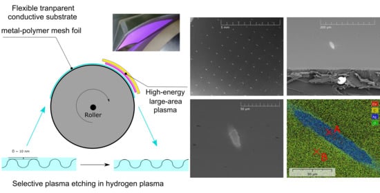
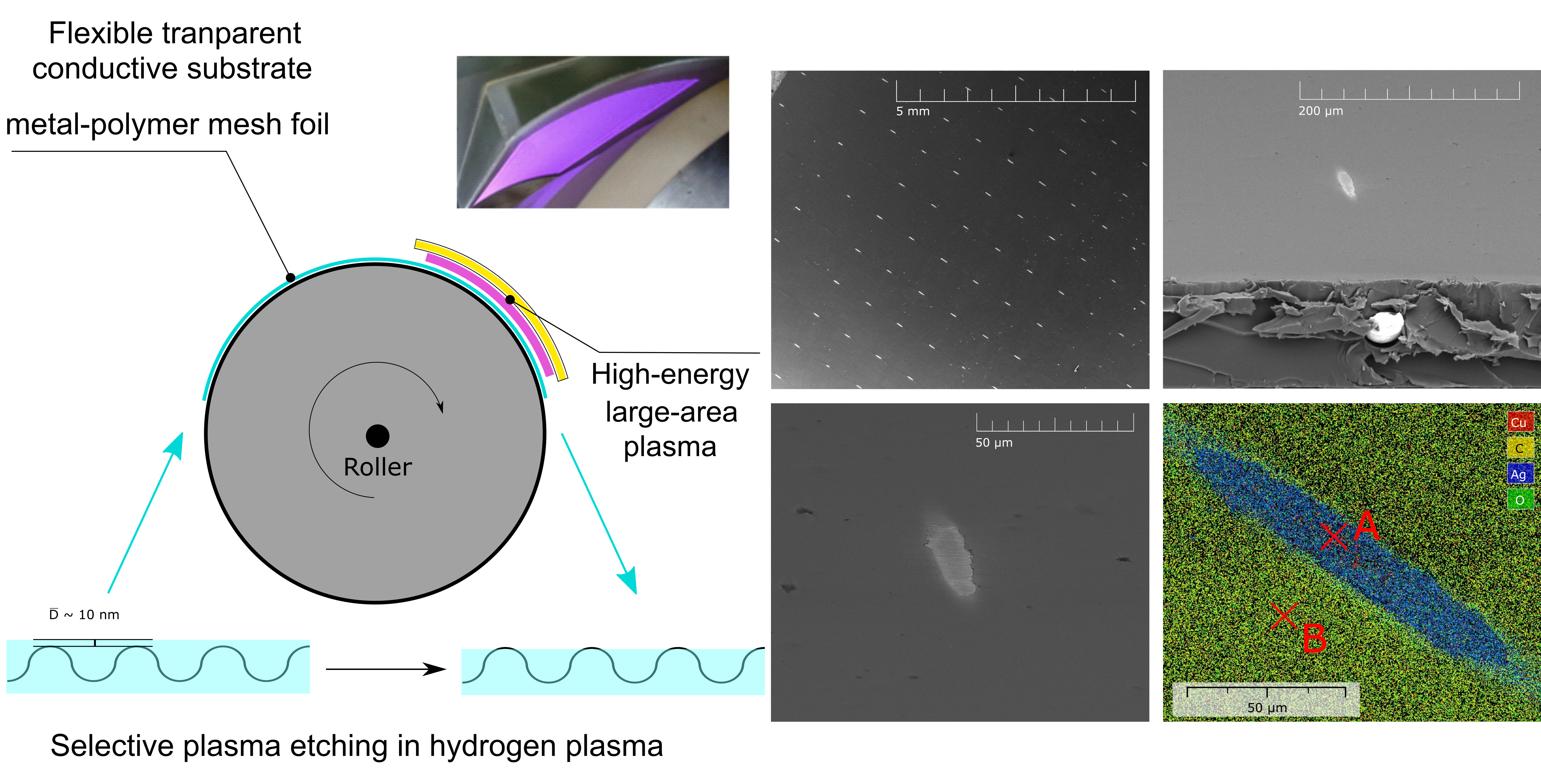
2. Materials and Methods

Plasma etching was performed on a composite mesh foil (Sefar AG, Thal, Switzerland), consisting of a grid of polymer and metal wires embedded in a polymer PMMA foil. The thickness of the mesh foil was 100 µm. Metal wires, from copper, of thickness 40 µm were coated with a thin 1 µm thick layer of silver. The metal wires embedded in the foil were oriented longitudinally to the machine direction of the plasma treater.
Figure 1 shows a reactor designed for roll-to-roll treatment and based on diffuse coplanar surface barrier discharge with a concavely curved alumina ceramics used to etch polymer mesh samples by non-thermal, low temperature (<80 °C) atmospheric pressure plasma. A 0.3-mm thin plasma layer with surface power density 2.5 W cm−2 was generated in pure nitrogen and pure hydrogen (both 99.998%, Messer Technogas, Prague, Czech Republic) and its mixtures (5% and 50% of H2 in N2) at a flow rate of 3.5 L/min. Plasma treatment in ambient air was done in a closed reactor without the flow of working gas. The discharge was fed by a sinusoidal high-frequency high voltage (15 kHz) signal at input power 400 W. The area of a thin layer of DCSBD plasma was 195 mm × 80 mm. To mimic a roll-to-roll plasma etching conditions, the sample of 15 cm × 20 cm size was attached to the metal roller covered by a rubber with a diameter of 296 mm. Plasma treatment time in the range 0.25–3 s was changed by the setting of circumferential speed of the roller. The distance H between the sample surface and the concave DCSBD electrode surface was set to 0.35 mm. The samples were studied using SEM, EDX and confocal microscopy.
Confocal Laser Microscope (LEXT OLS4000 3D Laser Measuring Microscope) was employed to observe the changes on plasma etched samples. Scanning Electron Microscopy with Energy dispersive X-ray Analysis using a MIRA3 device (TESCAN, Brno, Czech Republic) was used to reveal the changes in surface morphology, and chemical changes of plasma treated samples. SEM micrographs were taken using the accelerating voltage 10 kV; the edge of the samples was observed at accelerating voltage 30 kV. All samples were coated with a 10-nm layer of Au before the SEM analysis.

3. Results

3.1. Plasma Etching of Thin Surface Polymer Layer

Pure atmospheric-pressure hydrogen plasma was employed to etch out the polymer film from the surface of mesh foil and to expose free metal wire surface (Figure 2). The thickness of the polymer layer at the thinnest point over the top of a metal wire was ranging in the order of 1 nm up to 100 nm. The removal of a thin surface polymer film is important to make conductive connection sites on the surface before next processing steps.
As seen in Figure 3, already a short plasma exposure time of 1 s can expose “isles” of free metal surface. Figure 3a shows the surface of the untreated sample. More bright, uncovered metal areas are visible in Figure 3b showing etched surface with details on single uncovered wires in Figure 3c,d. Both SEM images Figure 3a,b were taken at the same magnification 26×, working distance 15.0 mm and view field 10.7 mm at accelerating voltage 15.0 kV. The shorter exposure times (0.25 s and 0.5 s) led to the etching of surface polymer film, however, not all metal wires tops were exposed (uncovered) on the surface after such short plasma etchings.
Figure 4 shows SEM micrograph of a single uncovered wire after 1 s etching in pure H2 plasma. The SEM image is shown using secondary electrons (SE image) and also back-scattered electrons (BSE image).
Secondary electrons originate within a few nanometers from the sample surface [20]. Therefore, SE image shows the best the topography of the analyzed surface. Since heavy elements in the specimen reflect or backscatter electrons more effectively than the light elements, the atoms with a high atomic number appear brighter in the BSE image [20]. Backscattered electrons can be then used to detect contrast between areas with different chemical compositions. As seen in Figure 4 (BSE image), we can distinguish a bright uncover metal wire from the dark area composed of light polymer material.
Figure 5a,b shows the EDX line scans in lateral and longitudinal direction, respectively. As observed, surface polymer film was successfully removed uncovering the metal wire. Figure 6 shows composite element map of single wire indicating removal of polymer on the entire area of the uncovered wire. In the area of uncovered wire a strong signal of silver was evident, while only a small signal of copper indicating concentration of copper less than 0.5 wt.% was discernible (Figure 6 and Table 1). This indicates that the thin polymer film was removed from the area above the wire without damage of metal wire and its silver coating. The presence of carbon and a small concentration of oxygen in the area of uncovered wire as shown in Figure 5 can be explained by the surface contamination during the manipulation with the sample, when the sample was exposed to air after the plasma etching for several hours before the SEM EDX analysis. We suppose that this is also the reason for the higher concentration of carbon in the plasma exposed area of pure polymer compared to the value expected on the clean PMMA surface.

3.2. Selectivity of Hydrogen Plasma Etching

Figure 7 shows the details on the tops of uncovered metal wires after 3-s etching in ambient air plasma (a), nitrogen plasma (b), H2/N2 plasma (50%) (c), hydrogen plasma (d) and after 1-s etching in hydrogen plasma (e). As seen, ambient air plasma and nitrogen plasma led, besides the polymer etching, also to significant damages of the metal wires. Sample (c) treated in a mixture of hydrogen and nitrogen showed a degradation of polymer around uncovered metal tops. Sample (d) was multiple treated with short exposures of 0.25 s and total treatment time 3.0 s (with a dead time 2.7 s between each plasma exposure and 29.7 s in total). The reason for such non-continuous treatment was to decrease the thermal load on the thermally sensitive PMMA-based substrate and to prevent the unwanted effect of plasma over-exposure. Generally, it is evident that only the pure DCSBD hydrogen plasma has the capability of selective etching of thin surface polymer accompanied by just a negligible effect on the metal wires in the polymer mesh foil.

3.3. The Effect of the Sample Distance from the DCSBD Plasma Layer on Plasma Etching

Diffuse coplanar surface barrier discharge in a configuration with a concavely curved electrode arrangement is capable of generation of visually almost uniform diffuse plasma layer of some 0.3-mm effective thickness. In this work, the polymer foil was treated at a distance in the range 0.2–0.6 mm from the alumina ceramics.
It was already reported that DCSBD plasma consists of optically two distinctive regions: (i) diffuse plasma located directly above strip electrodes and (ii) the gentle streamer filaments located above the space between the electrodes [21]. It was shown that the decreasing gap between the conductive sample and the ceramics with the plasma layer led to the change of generated plasma—extinction of filamentary plasma was observed.
Figure 8 summarizes the results of 1 s plasma etching in pure H2 plasma at distances 0.2–0.6 mm. Original SEM images appear in Figure 9. As observed, there is an optimal distance for plasma etching of polymer mesh foil. If the distance is larger than 0.5 mm, the surface of the sample is disrupted by the streamers which are generated perpendicularly to its surface. This results in inhomogeneous etching and uncovering the metal wire only at a small area, as seen in Figure 9d, for the distance of 0.6 mm, together with the rough transition zone between polymeric and metal area. If there was a small gap between the sample and the plasma layer, the streamers could not be creating, and plasma was generated preferably in the diffuse mode. On the other hand, a small gap between the sample and the ceramics with the electrode system led to an increase of thermal heating of the polymer. As seen from SEM micrograph in Figure 9a, thermal heating may cause a cracking of the polymer in the transition zone around a free metal wire. A roughening of the wire and sputtering of the thin silver coating from the wire was observed.

3.4. The Effect of the Treatment Time on Plasma Etching

As reported, only 1 s exposure to H2 plasma can etch the surface of polymer film sufficiently to uncover of the metal wires tops. The exposures less than 0.5 s resulted in not completed etching when not all metal wires tops were completely free of the polymer film. The longer etching in hydrogen DCSBD plasma resulted in the cracks in the polymer around the uncovered wires tops and delamination of the polymer as seen in Figure 10. This damage was caused by thermal degradation of the polymer at longer exposures in plasma. The benefit of using 100% hydrogen plasma treatment is also in a significantly lower thermal impact on the surface compared to 100% nitrogen atmospheric plasma or H2/N2 gas mixture due to the absence of any heavy particle. A surface power density of 100% hydrogen plasma was about 2.5 W cm−2, whereas the electron density and electron temperature were 1.3 × 1016 cm−3 and 19 × 103 K respectively [15].
It was found that the unwanted thermal degradation of polymer foil can be prevented by applying a multiple short-time plasma exposure on the etched surface. This is apparent from Figure 11 comparing the samples etched for 3 s using single 3 s plasma exposure (Figure 11a) and the multiple very short exposures (12 × 0.25 s) in hydrogen plasma (Figure 11b).

4. Discussion

As confirmed by SEM/EDX analysis, the atmospheric pressure DCSBD plasmas generated in ambient air, pure nitrogen, pure hydrogen and in mixtures of nitrogen with hydrogen is capable of etching of PMMA polymer layers on polymer-metal mesh substrates. However, a strong degradation of the polymer substrate and also the significant damages to the metal wires were observed. On the other hand, it was found that using a short, 1 s exposure of the polymer surface to the pure hydrogen plasma it is possible to etch selectively the surface polymer layer and to uncover the metal wires without damaging them. As a consequence, we conclude that the pure hydrogen DCSBD plasma can be used for the fast, selective etching of the polymer film surface without any destruction of the metal wires. We observed that the etching mechanism strongly depends on the parameters such as treatment time and the distance of the sample from discharge. Therefore, the effect of these parameters was discussed in more details.
The application of pure hydrogen plasma raises the questions about the safety of the process. As in any other activity/process, it is necessary to find a trade-off between the safety, the process performance, and the product requirements. The presented plasma modification method might be improved by localized feeding of working gas just into the very narrow region where the plasma is generated. Such technical solution would enable to decrease the working gas consumption and together with smaller volume of (dangerous) working gas presented in the reactor chamber this would lead to higher safety of the entire process and whole device.
In comparison to standard mechanical abrasion and low-pressure plasma etching of studied flexible polymer-metal mesh substrate, the presented method utilizing atmospheric DCSBD plasma is easily scalable and compatible with roll-to-roll processing of large-area substrates. To sum up, we conclude that the DCSBD plasma sources can be used for fast, large-area, roll-to-roll, selective plasma etching of complex materials like flexible transparent conductive substrates which can be applied e.g., for flexible photovoltaic applications and other emerging technologies.

Author Contributions

Conceptualization, M.Č. and D.K.; investigation, R.K., J.J., M.Z. and J.K.; writing—original draft preparation, R.K.; writing—review and editing, R.K., D.K. and M.Č. All authors have read and agreed to the published version of the manuscript.

Funding

This research was supported by project LM2018097 funded by the Ministry of Education, Youth and Sports of the Czech Republic and project TJ01000327 funded by the Technology Agency of the Czech Republic.

Acknowledgments

The authors thank to Peter Chabrecek and SEFAR AG (Switzerland) for providing the polymer mesh substrate. Thanks belongs also to Jan Čech and Dana Skácelová both from CEPLANT, MU Brno for carrying out the trial experiments on selective etching of small polymer mesh samples providing by SEFAR AG.

Conflicts of Interest

The authors declare no conflict of interest.

References

  1. Puliyalil, H.; Cvelbar, U. Selective plasma etching of polymeric substrates for advanced Applications. Nanomaterial 2016, 6, 108. [Google Scholar] [CrossRef] [PubMed] [Green Version]
  2. Sarra-Bournet, C.; Ayotte, G.; Turgeon, S.; Massines, F.; Laroche, G. Effects of chemical composition and the addition of H2 in a N2 atmospheric pressure dielectric barrier discharge on polymer surface functionalization. Langmuir 2009, 25, 9432–9440. [Google Scholar] [CrossRef] [PubMed]
  3. Vargo, T.G.; Gardella, J.A.; Meyer, A.E.; Baier, R.E. Hydrogen/liquid vapor radio frequency glow discharge plasma oxidation/hydrolysis of expanded poly(tetrafluoroethylene) (ePTFE) and poly (vinylidene fluoride) (PVDF) surfaces. J. Polym. Sci. Part A Polym. Chem. 1991, 29, 555–570. [Google Scholar] [CrossRef]
  4. Cunge, G.; Ferrah, D.; Petit-Etienne, C.; Davydova, A.; Okuno, H.; Kalita, D.; Bouchiat, V.; Renault, O. Dry efficient cleaning of poly-methyl-methacrylate residues from graphene with high-density H2 and H2-N2 plasmas. J. Appl. Phys. 2015, 118, 123302. [Google Scholar] [CrossRef]
  5. Xie, L.; Jiao, L.; Dai, H. Selective etching of graphene edges by hydrogen plasma. J. Am. Chem. Soc. 2010, 132, 14751–14753. [Google Scholar] [CrossRef] [PubMed]
  6. Hou, P.-X.; Li, W.-S.; Zhao, S.; Li, G.-X.; Shi, C.; Liu, C.; Cheng, H.-M. Preparation of metallic single-wall carbon nanotubes by selective etching. ACS Nano 2014, 8, 7156–7162. [Google Scholar] [CrossRef] [PubMed]
  7. Zhang, G.; Qi, P.; Wang, X.; Lu, Y.; Li, X.; Tu, R.; Bangsaruntip, S.; Mann, D.; Zhang, L.; Dai, H. Selective etching of metallic carbon nanotubes by gas-phase reaction. Science 2006, 314, 974–977. [Google Scholar] [CrossRef] [PubMed] [Green Version]
  8. Šimor, M.; Ráheľ, J.; Vojtek, P.; Černák, M.; Brablec, A. Atmospheric-pressure diffuse coplanar surface discharge for surface treatments. Appl. Phys. Lett. 2002, 81, 2716–2718. [Google Scholar] [CrossRef]
  9. Georghiou, G.E.; Papadakis, A.P.; Morrow, R.; Metaxas, A.C. Numerical modelling of atmospheric pressure gas discharges leading to plasma production. J. Phys. D Appl. Phys. 2005, 38, R303–R328. [Google Scholar] [CrossRef]
  10. Roth, J.R. Industrial Plasma Engineering: Volume 2: Applications to Nonthermal Plasma Processing, 1st ed.; CRC Press: Boca Raton, FL, USA, 2001. [Google Scholar]
  11. Kuzminova, A.; Kretková, T.; Kylián, O.; Hanuš, J.; Khalakhan, I.; Prukner, V.; Doležalová, E.; Šimek, M.; Biederman, H. Etching of polymers, proteins and bacterial spores by atmospheric pressure DBD plasma in air. J. Phys. D Appl. Phys. 2017, 50, 135201. [Google Scholar] [CrossRef]
  12. Kwon, Y.-T.; Lee, Y.-I.; Kim, S.; Lee, K.-J.; Choa, Y.-H. Full densification of inkjet-printed copper conductive tracks on a flexible substrate utilizing a hydrogen plasma sintering. Appl. Surf. Sci. 2017, 396, 1239–1244. [Google Scholar] [CrossRef]
  13. Černák, M.; Kováčik, D.; Ráheľ, J.; Sťahel, P.; Zahoranová, A.; Kubincová, J.; Tóth, A.; Černáková, Ľ. Generation of a high-density highly non-equilibrium air plasma for high-speed large-area flat surface processing. Plasma Phys. Control Fusion 2011, 53, 124031. [Google Scholar] [CrossRef]
  14. Homola, T.; Pospisil, J.; Krumpolec, R.; Souček, P.; Dzik, P.; Weiter, M.; Černák, M. Atmospheric Dry Hydrogen Plasma Reduction of Inkjet-Printed Flexible Graphene Oxide Electrodes. ChemSusChem. 2018, 11, 941–947. [Google Scholar] [CrossRef] [PubMed]
  15. Prysiazhnyi, V.; Brablec, A.; Čech, J.; Stupavská, M.; Černák, M. Generation of Large-Area Highly-Nonequlibrium Plasma in Pure Hydrogen at Atmospheric Pressure. Contrib. Plasma Phys. 2014, 54, 138–144. [Google Scholar] [CrossRef]
  16. Krumpolec, R.; Čech, J.; Jurmanová, J.; Ďurina, P.; Černák, M. Atmospheric pressure plasma etching of silicon dioxide using diffuse coplanar surface barrier discharge generated in pure hydrogen. Surf. Coatings Technol. 2017, 309, 301–308. [Google Scholar] [CrossRef]
  17. Jirásek, V.; Čech, J.; Kozak, H.; Artemenko, A.; Černák, M.; Kromka, A. Plasma treatment of detonation and HPHT nanodiamonds in diffuse coplanar surface barrier discharge in H2/N2 flow. Phys. Status Solidi (A) 2016, 213, 2680–2686. [Google Scholar] [CrossRef]
  18. Tučeková, Z.; Kelar, J.; Doubková, Z.; Krumpolec, R. Structuring of polymethylmethacrylate substrates by reducing plasma. In Book of Contribution Papers, Proceedings of the 22nd Symp. Appl. Plasma Process. (SAPP XXII) 11th EU-Japan Jt. Symp. Plasma Process, Štrbské Pleso, Slovakia, 18–24 January 2019; Medvecká, V., Országh, J., Papp, P., Matejčík, Š., Eds.; Society for Plasma Research and Applications in Cooperation with Library and Publishing Centre CU: Bratislava, Slovakia, 2019; pp. 269–272. [Google Scholar]
  19. Doubková, Z.; Tučeková, Z.; Kelar, J.; Krumpolec, R.; Zemánek, M. Modification of various polymer surfaces using atmospheric pressure reducing plasma. In Proceedings of the NANOCON 2018, Brno, Czech Republic, 17–19 October 2018; Peer Rev. TANGER Ltd.: Ostrava, Czech Republic, 2019; pp. 688–693. Available online: https://www.nanocon.eu/files/uploads/01/NANOCON2018-ConferenceProceedings_content.pdf (accessed on 15 October 2020).
  20. Egerton, R.F. Physical Principles of Electron Microscopy; Springer-Verlag US: Boston, MA, USA, 2005; ISBN 978-0-387-25800-3. [Google Scholar]
  21. Homola, T.; Matoušek, J.; Medvecká, V.; Zahoranová, A.; Kormunda, M.; Kováčik, D.; Černák, M. Atmospheric pressure diffuse plasma in ambient air for ITO surface cleaning. Appl. Surf. Sci. 2012, 258, 7135–7139. [Google Scholar] [CrossRef]
Figure 1. Reactor based on diffuse coplanar surface barrier discharge (DCSBD) with concavely curved alumina ceramics for roll-to-roll treatment of flexible substrates. 1—Concavely curved DCSBD unit; 2—DCSBD plasma; 3—roller; 4—sample; 5—reactor chamber; 6—gas inlet; 7—gas outlet.
Applsci 10 07356 g001
Figure 2. Schematic sketch of plasma etching. The average thickness of the etched polymer over the wire tops was about 10 nm. 1—polymer foil; 2—mesh of polymer and metal wires; 3—metal wire; 4—uncovered metal wires tops.
Applsci 10 07356 g002
Figure 3. The surface of (a) untreated mesh foil and (b) the mesh foil after H2 plasma etching (1 s) with details on cross-section and upper surface of exposed wires (c) and upper surface detail (d). The distance of the sample surface from the surface of concave DCSBD electrode system was H = 0.35 mm.
Applsci 10 07356 g003
Figure 4. SEM micrograph of the uncovered wire top after 1 s H2 plasma exposure (distance H = 0.35 mm).
Applsci 10 07356 g004
Figure 5. Longitudinal (a) and lateral (b) EDX line-scans taken on single uncovered wire on sample treated 1 s in H2 plasma (distance H = 0.35 mm).
Applsci 10 07356 g005
Figure 6. Composite element map in the area of single uncovered wire. C—yellow, O—green, Ag—blue, Cu—red (distance 0.35 mm, treatment time 1 s).
Applsci 10 07356 g006
Figure 7. Exposed metal wires after etching in (a) ambient air plasma, (b) nitrogen plasma, (c) H2/N2 plasma (50%) and (d,e) hydrogen plasma. Samples (ad): treatment time 3 s (12 × 0.25 s for sample (d)); sample (e): treatment time 1 s in 100% hydrogen plasma.
Applsci 10 07356 g007
Figure 8. The effect of the sample distance from DCSBD plasma layer, and H2 plasma treatment time on the mechanism of the etching of polymer mesh foil.
Applsci 10 07356 g008
Figure 9. SEM micrographs of free metal wires after 1 s plasma etching in pure H2 plasma at distance of 0.2 mm (a), 0.3 mm (b), 0.4 mm (c) and 0.6 mm (d). Top row—SE image; bottom row—BSE image.
Applsci 10 07356 g009
Figure 10. SEM micrographs of free metal wires treated for (a) 1 s (b), 2 s (c) and 3 s at distance H = 0.3 mm. Top row—SE image; bottom row—BSE image.
Applsci 10 07356 g010
Figure 11. SEM micrographs of metal wires after 3 s plasma etching in pure H2 plasma at distance H = 0.6 mm for single 3 s plasma exposure (a) and the multiple very short exposures (12 × 0.25 s) (b). Top row—SE image; bottom row—BSE image.
Applsci 10 07356 g011
Table 1. Concentration of Carbon, Oxygen, Silver and Copper on the sample after 1 s etching at distance 0.35 mm measured in the areas A and B as shown in Figure 6.
ElementConcentration (at.%)
AB
CCarbon34.592
OOxygen6.58
AgSilver58.5-
CuCopper0.5-
Publisher’s Note: MDPI stays neutral with regard to jurisdictional claims in published maps and institutional affiliations.

