Article

An Improved Investigation into the Effects of the Temperature-Dependent Parasitic Elements on the Losses of SiC MOSFETs

1
Department of Electrical Engineering, University of Shanghai for Science and Technology, Shanghai 200082, China
2
College of Electrical and Information Engineering, Zhengzhou University of Light Industry, Henan 450000, China
*
Author to whom correspondence should be addressed.
Appl. Sci. 2020, 10(20), 7192; https://doi.org/10.3390/app10207192
Submission received: 14 September 2020 / Revised: 2 October 2020 / Accepted: 12 October 2020 / Published: 15 October 2020

Abstract

:

Featured Application

The conclusion of this paper could serve as an important basis for the design guidelines of fast switching power converters.

Abstract

This paper presents an improved investigation into the effects of temperature-dependent parasitic elements on the silicon carbide (SiC) MOSFET power losses. Based on the physical knowledge of MOSFET, a circuit-level loss analytical model is proposed, which takes the parasitic elements of the power devices and the stray inductances of the Printed Circuit Board (PCB) traces into consideration. The state equations derived from the equivalent circuit of each stage is solved by iteration to calculate the loss in the switching transients. In order to study the temperature characteristic completely, the key parameters needed in the calculation are extracted from power device test platform based on Agilent B1505A. The loss assessment of the proposed analytical model with varied elements has been successfully substantiated by the experimental results of a 400-V, 15-A double-pulse-test bench. Finally, some practical knowledge about loss mechanisms is given to help estimate the power losses and optimize the efficiency of power converters.

1. Introduction

In recent years, silicon carbide (SiC) has attracted extensive attention and has been gradually applied to power semiconductor devices due to its higher breakdown electric field, electron saturation velocity and thermal conductivity than conventional silicon (Si) materials [1,2,3,4,5]. In addition, increasing switching frequency has always been a common method to push up the power density and facilitate the miniaturization of switching converters by reducing the size of the passive components [6,7]. With a significant increase in switching speed, the effect of parasitic elements that mainly result from power semiconductor devices and PCB traces on switching performance can no longer be ignored and the losses become a crucial factor that determines the converter efficiency. Therefore, it is necessary to accurately calculate the loss of power devices and analyze the effects of the parasitic elements on it, helping designers to acquire in-depth knowledge of the switching loss mechanisms. There is considerable research in this filed. As discussed in [8], basically, investigation into loss can be classified into three categories. They are physical model, behavioral model, and analytical model (also called mathematical model).
Based on the knowledge of semiconductor physics and microelectronics, the physical model solves the characteristic expression of power devices by conducting the finite element analysis (FEA) [9,10,11,12]. The simulation results of physical model match the experimental results very well. However, this kind of model needs comprehensive parameters of the power device, such as gate oxide thickness, doping concentration in the channel, electron mobility, etc., which are difficult to obtain and the modeling process is rather complex and time-consuming, which is not suitable for circuit-level simulation.
The behavior model is widely used in the loss analysis because it has a good trade-off between the accuracy and simulation time. Based on the values obtained from parameter extraction (normally, device manufacturer provides these data or models on their website), the effect of parasitic elements including the junction capacitances of power devices and the stray inductances of the PCB traces on switching loss can be analyzed by circuit simulation software, e.g., PSpice or Saber, in which behavioral model of the MOSFET is used [13,14,15]. In [14], with specific modifications of the conventional Si power MOSFET model based on PSpice, an improved behavioral model is proposed for 10-kV SiC MOSFETs to validly predict switching loss. However, it cannot suffice to explain the switching loss mechanisms of the power device behind the simulation results.
The last method is the analytical model [16,17,18,19,20,21,22,23,24]. Generally, the switching loss expressions are derived from different equivalent circuits according to different stages on switching transients. The simplest and classical analytical model is the piecewise linear model, which is easier to obtain and solve than the aforementioned two model. However, there are many limitations in such a model; for example, ([16]) the analytical model only considers the gate resistance and the junction capacitances (the switching process is equivalent to the charging and discharging process of the RC circuit). In practice, especially in high-frequency operation, the effect of parasitic inductances cannot be totally ignored. Other analytical models that consider both junction capacitances and parasitic inductances have also been proposed. The effect of the parasitic elements on switching performance in low-voltage operation (the voltage lower than 40 V) has been extensively discussed in [17,18,19,20]. In low-voltage operation, the drain-source voltage may reach zero before the drain current reaches the steady-state value during the turn-on transients and the drain current may drop to zero before the drain-source voltage reaches bus voltage during the turn-off transients [19]. However, these particular cases will hardly happen to high-voltage MOSFETs. The analytical model of [21] considers the MOSFET–Snubber–Diode (MSD) configuration, whereas it treats the trans-conductance and the threshold voltage as a constant. In [23,24], the parasitic elements of the analytical model are extracted from the datasheet of the device vendor, but these models cannot reflect the temperature characteristics of the parasitic elements of the power devices. As a result, there are a lot of limitations in these analytical models.
For the sake of accuracy and computational efficiency, an improved analytical model that considers temperature-dependent parasitic elements of SiC MOSFET and the interaction between exterior parasitic inductances of PCB traces will be proposed. The paper is organized as follows: in Section 2, the basis of modeling is given. In Section 3, the turn-on and turn-off transients of the SiC MOSFET are divided into five stages, respectively, and then the state equations are derived from the equivalent circuits of each stages. In Section 4, a power device analysis platform is built to obtain the detailed temperature characteristics of the parasitic elements. In Section 5, the calculation results of this proposed analytical model will be verified by comparison with the experimental results of a 400-V, 15-A double-pulse test bench, then, the effects of the parasitic elements on loss will be comprehensive explained. Finally, a conclusion that can help engineer to design high-frequency power converters and minimize switching loss will be given in the Section 6.

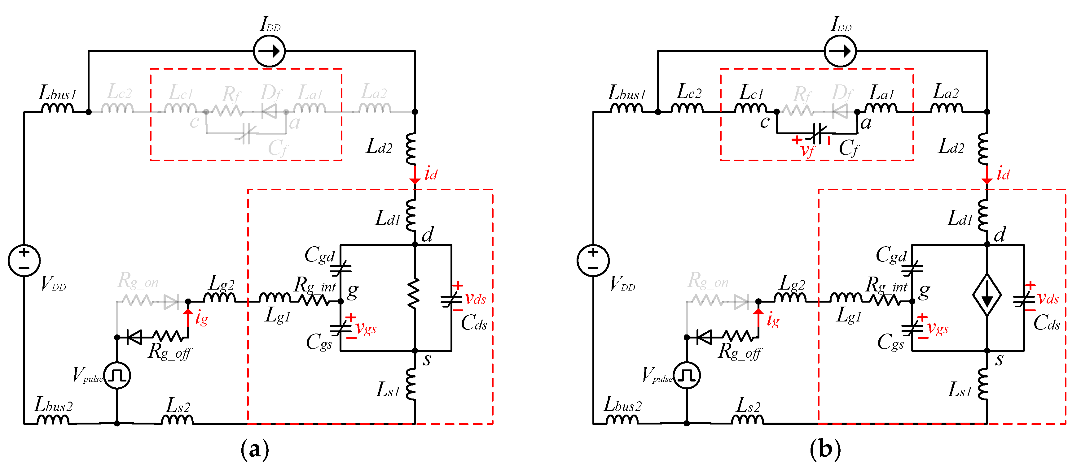
2. The Basis of the Analytical Model

Figure 1 shows a simplified physical structure of Vertical Double-diffused MOSFET (VDMOSFET) considering the discrete package. There is an internal resistance due to the gate contact. The pad parasitic inductances and the internal bonding between the carbon silicon die and the package pads, which are relevant to the package technology, contribute to the total parasitic inductance in the power device. The only viable alternative to further lower the parasitic inductances is to concurrently address the underlying package problem, using clip lead or sandwich package assembly methods to eliminate bond wires while maximizing the ratio of die area to package footprint [25]. As a unipolar device, the dynamic characteristics of SiC MOSFET are mainly determined by the charging and discharging process of the junction capacitances which are composed of oxide capacitances and depletion edge capacitances [26]. The width of depletion edge is related to the applied voltage between drain terminal and source terminal, so that the value of the junction capacitances is nonlinear. When a positive voltage applied between the gate terminal and source terminal, the depletion region gets wider towards the body, and it begins to drag the free electrons to the interface. As the density of the free holes of the body and the density of the free electrons of the interface becomes equal, the free electron layer is called the inversion layer (N channel).
Based on the above knowledge, the equivalent circuit of the MOSFET is obtained, as shown in Figure 2. The junction capacitances are represented by three nonlinear capacitances connected in parallel with each internal node. The parasitic inductances in series in each terminal of the device (the gate terminal also includes the internal resistance). The channel is the key element of modeling, which determines the accuracy of the model and should be carefully considered. The equivalent of the channel in the switching transients will be thoroughly discussed in the next section.

3. Analysis of the Switching Transients

The switching process of the MOSFET will be studied stage by stage in this section. A double-pulse test circuit is adopted for the modeling of MOSFET switching transients, as shown in Figure 3. The input is a constant voltage source VDD and the load is a clamped-inductive load which can provide a constant current IDD. The gate signal Vpulse is assumed to flip between VSS and VGG with zero rise time and fall time in the analysis. In order to investigate the switching process better, two different external gate resistances Rg_on and Rg_off are used in the turn-on transients and turn-off transients, respectively. Similar to the MOSFET, the freewheeling diode is modeled by two parasitic inductances Lc_1 and La_1 and a parasitic resistance Rf in series with an ideal diode Df, and then in parallel with a nonlinear junction capacitance Cf. In addition to these power devices, there also are a lot of stray inductances result from the PCB traces of the power loop, which are represented by Lbus1, Lbus2, Lc_2, La_2, Ld_2, Lg_2 and Ls_2. In order to simplify the model and the equations, some parameters are merged in the equivalent circuit. Ld1 = Ld_ext + Ld_int, Lg1 = Lg_ext + Lg_int and Ls1 = Ls_ext + Ls_int are denoted as the total parasitic inductances at each terminal of the MOSFET, respectively. It should be noted that the stray inductance of the ground lead of a measuring loop is hard to quantitatively analyze and its influence on the loss assessment can be ignored. Therefore, it was not considered in this model.

3.1. Turn-On Switching Transients

Stage 1 [t0–t1] turn-on delay time: Before the gate source voltage vgs reaches the threshold voltage Vth, the SiC MOSFET power device is still in the cut-off region. At this stage, the value of the drain current id is assumed to be zero. According to Figure 4a and Kirchhoff’s law, the following equations are obtained:
V G G = R G G i g + L g d i g d t + v g s + L s d i s d t
i g = C g s d v g s d t + C g d d v g d d t
i s = C g s d v g s d t + C d s d v d s d t
v g s = v g d + v d s
i g + i d = i s
where RGG = Rg_on + Rg_int, Lg = Lg1 + Lg2.
There are three independent state variables: the drain current ig, the gate-source voltage vgs and the drain-source voltage vds. The state equations derived from above equations are shown in Appendix A Equation (A1). As the power device is not activated, there is no switching loss Psw during this period.
Stage 2 [t1–t2] current rise time: When the gate source voltage vgs goes beyond the threshold voltage Vth, the conductive pass (channel) enabling the current flow begins to form. Due to the fast speed of the SiC MOSFET power device, the drain current id surges, which generates the induced voltage across the parasitic inductances. This induced voltage deservers special attention, as it determines whether the drain current (id) will rise to its full value IDD before or after the drain-source voltage vds drops to vgsVth (the boundary condition between the saturation region and the ohmic region of MOSFET). If the power device works in the saturation region, the channel of the SiC MOSFET can be equivalent to a voltage-controlled current source (the relationship between the channel current ich and gate-source voltage vgs is governed by (6)), otherwise it can be equivalent to a nonlinear resistance which is related to the junction temperature Tj and the drain current id. Both of them are discussed as follows.
i c h = g f ( v g s V t h )
where gf is trans-conductance of the SiC MOSFET, which is also nonlinear.
Case I: The MOSFET works in the saturation region. In this situation, as shown in Figure 4b, the drain current id consists of three parts: the channel current ich and the current flowing through the junction capacitor Cgd and Cds. The circuit equations can be expressed as:
V G G = R G G i g + L g d i g d t + v g s + L s ( d i d d t + d i g d t )
i g = ( C g s + C g d ) d v g s d t C g d d v d s d t
v d s = V D D v f L p d i d d t L s d i g d t
i d = g f ( v g s V t h ) + C d s d v d s d t C g d d ( v g s v d s ) d t
v f = R f ( i d I D D ) V f
where Lp = Lbus1 + Lbus2 + Lc + La + Ld + Ls, Lc = Lc1 + Lc2, La = La1 + La2, Ld = Ld1 + Ld2, Ls = Ls1 + Ls2.
Case II: The MOSFET works in ohmic region directly. As discussed above, the channel of MOSFET can be represented by a nonlinear resistance in this scenario. Therefore, (10) is changed to (12), and the rest remains unchanged.
i d = v d s R o n + C d s d v d s d t C g d d ( v g s v d s ) d t
A new independent state variable id appears in this stage compared to the previous one, and the state equations derived from the above equations are shown in Appendix A Equation (A3). This stage ends when the drain current id reaches the bus current IDD. The switching loss Esw expression in this period is as follows.
E ( Ι ) s w _ s 2 = t 1 t 2 i d v d s d t
However, a more appropriate switching loss analysis is to replace (13) with (14), taking into account the assumption that the junction capacitances of MOSFET are only lossless energy buffers. The discrepancy between the two types of calculation methods will be further elucidated in Section 5 with the experimental verification.
E ( Ι Ι ) s w _ s 2 = t 1 t 2 i c h v d s d t
Stage 3 [t2–t3] voltage falling time I: As the current is transferred to the SiC MOSFET, the SiC Schottky Diode (SBD) becomes capable of blocking the voltage; Figure 4c shows the equivalent circuit of this stage, and the drain-source voltage vds drops dramatically at the same time, if the case I occurs in the previous stage. The gate-source voltage vgs is maintained at the Miller Plateau, because the gate current ig is completely absorbed by the drain-source capacitance Cds without flowing to the gate-source capacitance Cgs. Although SBD features zero reverse recovery current, the drain current id continues to increase since the charging current of junction capacitance Cf of the SiC SBD. Therefore, (11) is replaced by (15), and the rest remains unchanged. A resonant period begins in this moment, which induced by the oscillations between Lp and Cf. This stage ends when drain-source voltage vds decreases to vgsVth.
d v f d t = i d I D D C f
There are five independent state variables: the drain current ig, the drain current id, the gate-source voltage vgs, the drain-source voltage vds and the free freewheeling diode voltage vf. The state equations at this stage are shown in Appendix A Equation (A4).
During this period, the two type of switching loss calculation as following:
E ( Ι ) s w _ s 3 = t 2 t 3 i d v d s d t
E ( Ι Ι ) s w _ s 3 = t 2 t 3 i c h v d s d t
Stage 4 [t3–t4] voltage falling time II: When the drain-source voltage vds decreases to vgsVth, the SiC MOSFET will come out of the saturation region and get into the ohmic region. As shown in Figure 4d, the channel is equivalent to a nonlinear resistance (also called on-state resistance) in this stage. Therefore, (10) is replaced by (18). The gate-source voltage vgs breaks out of the Miller Plateau and begins to increase again. The drain-source voltage vds drops slightly in this period, and the drain current id drops back to IDD simultaneously. The oscillations in the power loop will be damped by the stray resistance resulting from the PCB traces. In order to specify this point, a lumped resistance Rstray is added in the equivalent circuit, as same as the stray inductances, to compensate for the active power consumption and (9) should be replaced by (19). Once the drain-source voltage vds decreases to id·Ron, this stage ends and the channel can be seen as completely conductive.
i d = v d s R o n + C d s d v d s d t C g d d ( v g s v d s ) d t
v d s = V D D v f R s t r a y i d L p d i d d t L s d i g d t
The independent state variables at this stage remain unchanged and the state equations are shown in Appendix A Equation (A5). The switching loss in this period can be calculated as:
E ( Ι ) s w _ s 4 = t 3 t 4 i d v d s d t
E ( Ι Ι ) s w _ s 4 = t 3 t 4 i c h v d s d t
Stage 5 [t4–t5] On-State Operation: The gate current ig still continues to charge the gate-source capacitance Cgs until the gate-source voltage vgs reaches the positive drive voltage VGG. The state equations and the equivalent circuit are the same as the previous stage, while the loss at this stage is considered as conduction loss Econd and can be calculated as:
E c o n d 1 = t 4 t 5 i d 2 R o n d t

3.2. Turn-Off Switching Transients

It is known that the turn-off switching transients are a reversely symmetrical process of the turn-on switching transients, in which the channel can also be equivalent to a nonlinear resistance, voltage-controlled current source, or an open circuit. Therefore, some repeated equations are omitted in the derivation of the stage equations for the turn-off switching transients.
Stage 6 [t6–t7] Turn-Off Delay Time: Before the gate source voltage vgs reduces to the Miller Voltage Vmiller, which is governed by (23), the SiC MOSFET power device operates in the ohmic region. It is assumed that the drain current id remains unchanged (id = IDD) at this stage. As shown in Figure 5a, the gate-source capacitance and the gate-drain capacitance are being discharged through Rg and Ls. The circuit equations are shown from (24) to (26):
V m i l = I o g f + V t h
V S S = R S S i g + L g d i g d t + v g s + L s ( d i d d t + d i g d t )
i g = ( C g s + C g d ) d v g s d t C g d d v d s d t
i s = v d s R o n + C g s d v g s d t + C d s d v d s d t
where RSS = Rg_off + Rg_int.
As with the stage 1, there are three independent state variables: the drain current ig, the gate-source voltage vgs and the drain-source voltage vds, and the state equations derived from the above equations are shown in Appendix A Equation (A6). Since the device is still activated, the loss during this period is conduction loss Econd, which can be calculated as:
E c o n d 2 = t 5 t 6 i d 2 R o n d t
Stage 7 [t7–t8] Voltage Rising Time I: During this stage, the power device still works in the ohmic region until the drain-source voltage vds reaches vgsVth. Therefore, the drain current id stays constant at IDD and the gate-source voltage vgs (almost) remains at the Miller voltage. The equivalent circuit and equations during this period are the same as the previous one, while the loss during this period is regarded as the switching loss Esw and can be calculated as:
E ( Ι ) s w _ s 7 = t 6 t 7 i d v d s d t
E ( Ι Ι ) s w _ s 7 = t 6 t 7 i c h v d s d t
Stage 8 [t8–t9] Voltage Rising Time II: When the drain-source voltage vds reaches vgsVth, the device begins to operate in saturation region. Therefore, the channel is equivalent to a voltage-controlled current source, as shown in Figure 5b. The drain-source voltage vds continues to increase until the forward voltage vf of the SBD decreases to the forward voltage −Vf. The voltage slew rate will be faster than in the previous stage, since the value of junction capacitance significantly decreases with the increase in drain-source voltage vds. A part of IDD will be flowing through the freewheeling diode to discharge the Cf, which will be causing the drain current id drop. During this period, the channel current ich is also governed by (6). Hence the drain current id expression is changed to (10) and the rest of the circuit equations are the same as the stage 4 and the state equations are shown in Appendix A Equation (A8). During this period, the switching loss Esw is given by (30) and (31).
E ( Ι ) s w _ s 8 = t 7 t 8 i d v d s d t
E ( Ι Ι ) s w _ s 8 = t 7 t 8 i c h v d s d t
Stage 9 [t9–t10] Current Falling Time: When the freewheeling diode ceases to block the voltage, the current begins to divert from the MOSFET to the freewheeling diode rapidly, which will induce a voltage drop across the parasitic inductances and simultaneously incur a voltage overshoot on the drain-source voltage vds. Compare to the previous stage, the expression of the freewheeling diode voltage is replaced by (11) and the rest of circuit equations remain unchanged. This stage ends when the gate-source voltage vgs decreases to Vth. The equivalent circuit is shown in Figure 5c.
E ( Ι ) s w _ s 9 = t 8 t 9 i d v d s d t
E ( Ι Ι ) s w _ s 9 = t 8 t 9 i c h v d s d t
Stage 10 [t10–t11] Off-State Operation: After the gate-source voltage vgs decreases to Vth, the device works in the cut-off region. For a similar reason, a lumped resistance is added in the circuit (shown in Figure 5d). This stage ends, when the gate-source voltage vgs decreases to the negative drive voltage VSS. The state equations are shown in Appendix A Equation (A9) Since the channel is inactive, there is no power loss during this period. As discussed above, the power loss during the switching transient can be categorized and summarized as (34) to (37).
E ( Ι / Ι Ι ) s w _ o n = i = 2 4 E ( Ι / Ι Ι ) s w _ s i
E ( Ι / Ι Ι ) s w _ o f f = i = 7 9 E ( Ι / Ι Ι ) s w _ s i
E c o n d = E c o n d 1 + E c o n d 2
E ( Ι / Ι Ι ) t o t a l = E ( Ι / Ι Ι ) s w _ o n + E ( Ι / Ι Ι ) s w _ o f f + E c o n d

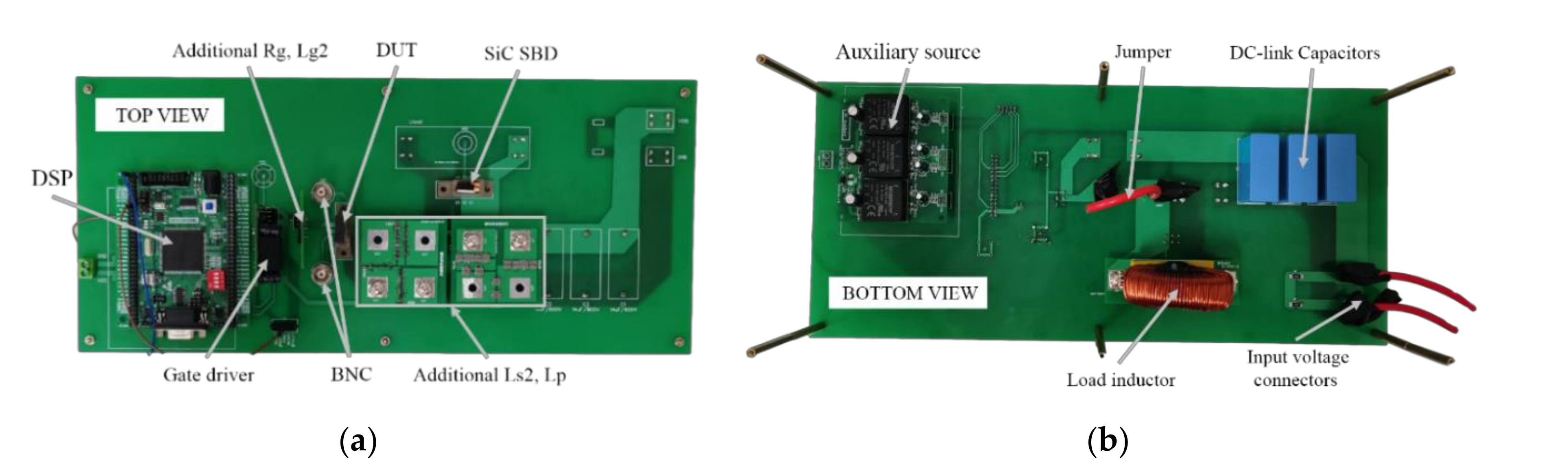
4. Experimental Setup

Based on the proposed analytical model, except for the operating condition VDD, IDD, VGG, and VSS, the parameters needed in the calculation are the junction capacitances Cgs, Cgd, Cgs and Cf, the stray inductances of the PCB traces Lbus, Lline, the parasitic inductances of the terminal Lg, Ld, Ls, La and Lc, and the static characteristic of power devices: the trans-conductance gf, the internal resistance Rg_int and Rf, the threshold voltage Vth, the forward voltage Vf, and on-state resistance Ron. Apart from the junction capacitances and the parasitic, stray inductances, all the other parameters are temperature dependent. Therefore, it is necessary to build a test platform for the measurement. The approaches to obtain these parameters can be divided into three categories.

4.1. Static Characteristic Test Platform

According to the standards of IEC 60747-8 [27] and datasheet of the device vendor [28,29], the static characteristic test platform based on Power Device Analyzer Curve Tracer (PDACT) Agilent B1505A with the heating plate was established to measure the static characteristic of SiC MOSFET C2M0025120D (Cree, 1200 V, 90 A) and SiC SBD C4D20120A (Cree, 1200 V, 90 A), as shown in Figure 6. Considering the materials and components that make up the package are not compatible with high temperature (usually lower than 175 °C) [30], the testing temperature ranges from 25 to 150 °C. It should be noted that the case temperature Tc obtained by infrared thermal camera is used to approximate the junction temperature Tj, since the latter is difficult to measure by conventional methods. The specific settings of each module are shown in Table 1.

4.2. ANSYS Q3D Extractor

A common approach to measure the value of the stray inductance is computational electromagnetics [31], which relies on finite-element analysis (FEA) simulation (e.g., ANSYS Q3D Extractor) to solve Maxwell’s equations through the PCB layout and component material information. The stray resistance and stray inductance, including both self-inductance and mutual-inductance, can be accurately extracted through this approach. However, in order to simplify the calculation, the mutual inductances are neglected in this analytical model.

4.3. Vector Network Analyzer

The parasitic inductance is mainly determined by the devices package. However, the above approach suffers from being time-consuming and having poor convergence, since the physical structure of a package is complex. There is a more practical approach which is based on Impedance Analyzer or Vector Network Analyzer (VNA) [32]. By calibrating the test system using a mathematical technique called vector error correction, VNA provides high measurement accuracy [33]. The power device is performed over a frequency range of 100 kHz to 200 MHz by Keysight VNA (E5061B). Since the MOSFET under zero applied voltage is equivalent to a second-order RLC circuit, as shown in Figure 7, it has a self-resonant frequency (SRF). The parasitic inductances and internal resistances can be calculated through its SRF [34]. The testing temperature also ranges from 25 to 150 °C.

5. Results

5.1. Experimental Results

The static characteristic parameters obtained from the above methods are shown in Figure 8e (the black scatter plot). All of these measured scatters require nonlinear fitting before they can be used for calculation. The extraction results of the stray inductances of PCB traces and the parasitic inductances of power device terminals are shown in Table 2, respectively. Due to the maximum difference of less than 5%, the parasitic inductances are treated as a constant (the average) in the later calculation. The internal resistance Rg_int and Rf obtained through VNA measuring are shown in Figure 8f while the others, such as Rs_int and Rd_int, are ignored in the proposed model since their values are very small.

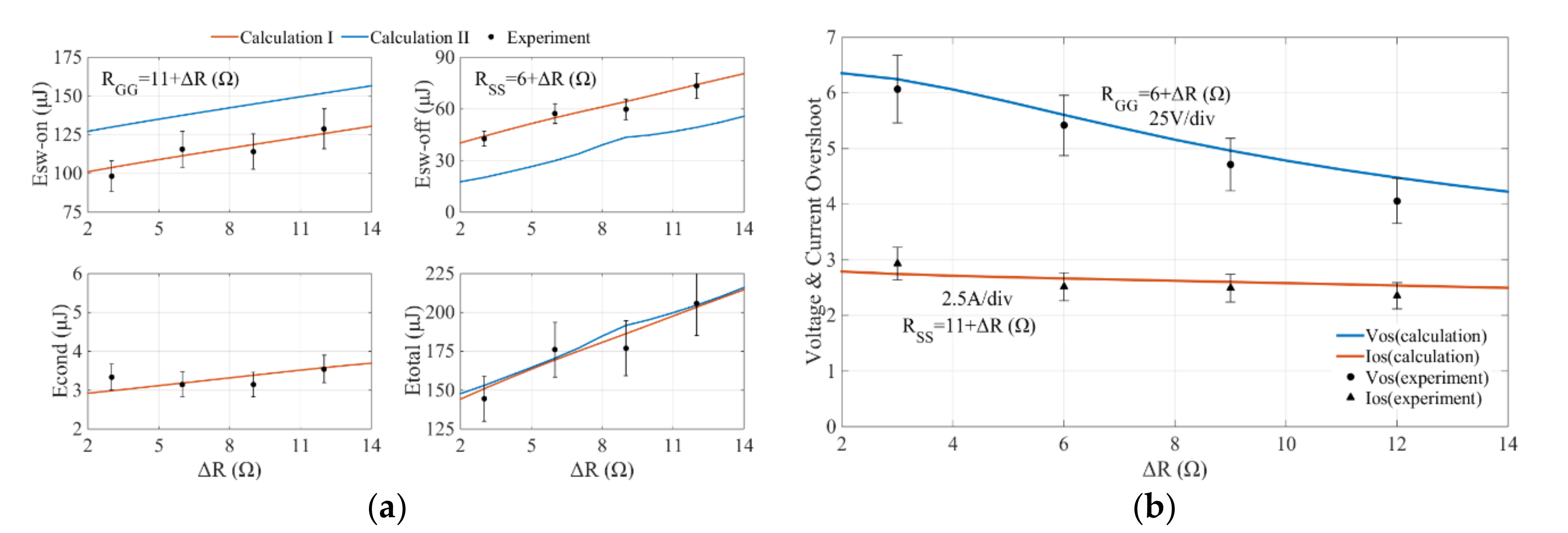
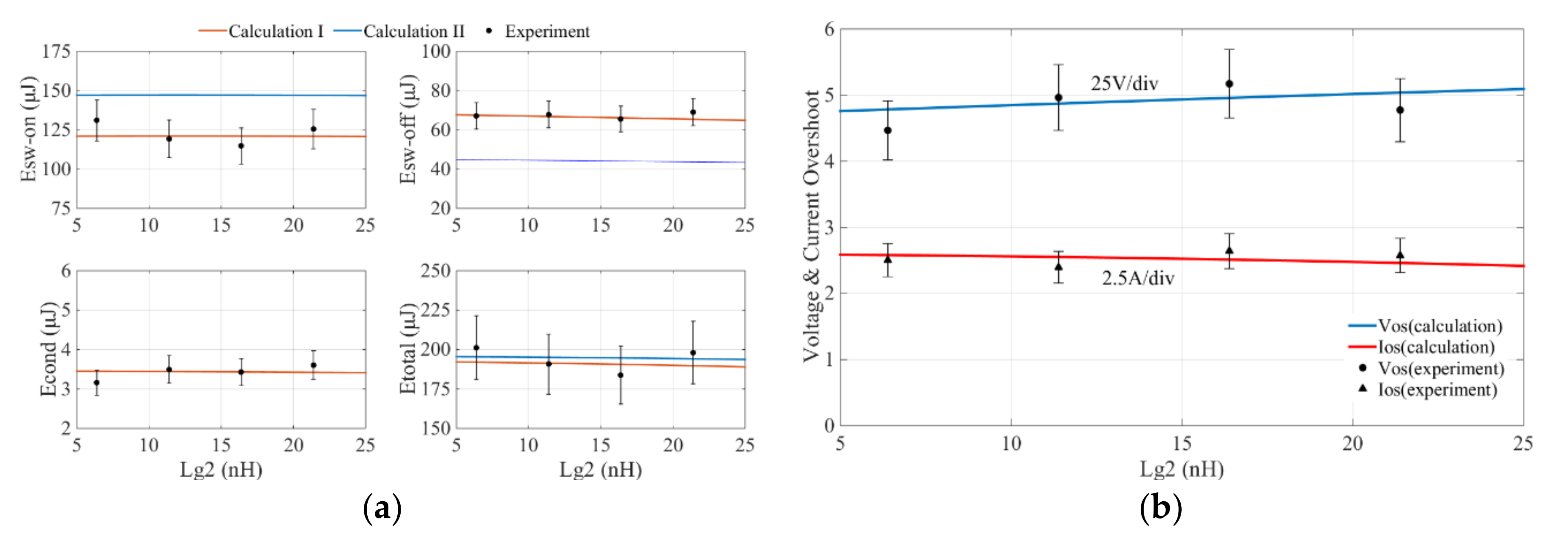
5.2. Fitting to the Key Parameters

For the sake of a trade-off between the precision and simplicity, the polynomial fitting is adopted to fit the static characteristic curve of the SiC MOSFET C2M0025120D. An appropriate polynomial order is chosen to ensure the R-squared (coefficient of determination, a goodness of fit) higher than 0.995. The trans-conductance gf and on-state resistance Ron can be regarded as a two-variable function of Vgs and Tj and function of id and Tj, respectively. The fitting equations are given in (38) and (39), the fitted curves are shown in the Figure 8a,b.
g f ( v g s , T j ) = p 00 + p 10 v g s + p 01 T j + p 20 v g s 2 + p 11 v g s T j + p 02 T j 2 + p 30 v g s 3 + p 21 v g s 2 T j + p 12 i d T j 2 + p 03 T d 3 + p 40 v g s 4   + p 31 v g s 3 T j + p 22 v g s 2 T j 2 + p 13 v g s T j 3 + p 04 T j 4
where p00 = −1.313, p10 = 2.74, p01 = 2.292 × 10⁻⁴, p20 = −1.287, p11 = −3.362 × 10⁻², p02 = −9.872 × 10⁻⁵, p30 = −0.2086, p21 = 9.167 × 10⁻³, p12 = 9.789 × 10⁻⁵, p03 = 6.437 × 10⁻⁸, p40 = −8.4 × 10⁻³, p31 = −5.352 × 10⁻⁴, p22 = −1.034 × 10⁻⁵, p13 = −8.058 × 10⁻⁸, p04 = 2.109 × 10⁻¹⁰.
R o n ( i d , T j ) = p 00 + p 10 i d + p 01 T j + p 20 i d 2 + p 11 i d T j + p 02 T j 2 + p 30 i d 3 + p 21 i d 2 T j + p 12 i d T j 2 + p 03 T d 3 + p 40 i d 4 + p 31 i d 3 T j + p 22 i d 2 T j 2 + p 13 i d T j 3 + p 04 T j 4
where p00 = 30.71, p10 = 0.03, p01 = −0.1388, p20 = 3.705 × 10⁻⁴, p11 = −2.019 × 10⁻⁴, p02 = 4.309 × 10⁻³, p30 = −1.091 × 10⁻⁸, p21 = −1.725 × 10⁻⁶, p12 = 2.894 × 10⁻⁶, p03 = −2.642 × 10⁻⁵, p40 = 6.933 × 10⁻⁹, p31 = −2.448 × 10⁻⁹, p22 = 2.817 × 10⁻⁹, p13 = −6.658 × 10⁻⁹, p04 = 6.943 × 10⁻⁸.
The threshold voltage Vth, the forward voltage Vf, the gate internal resistance Rg_int and the freewheeling resistance Rf can be regarded as a single-variable function of the junction temperature Tj. The fitting equations are given from (40) to (43) and the fitted curves are shown from Figure 8c–f.
V t h ( T j ) = 1.064 × 10 5 T j 2 0.006629 T j + 2.779
V f ( T j ) = 0.001509 T j + 1.012
R g _ int ( T j ) = p 1 T j 3 + p 2 T j 2 + p 3 T j + p 4
where p1 = 6.104 × 10⁻⁸, p2 = 7.835 × 10⁻⁶, p3 = −4.974 × 10⁻³, p4 = 1.524.
R f ( T j ) = 0.271 T j + 22.52
Nevertheless, polynomial does not perform well in the junction capacitance versus the applied voltage curve fitting. According to [35,36], the input capacitance Ciss was treated as two discrete values and (44) is adopted to characterize the nonlinearity of the output capacitance Coss and the reverse transfer capacitance Crss (see Table 3). The transform relationship between Ciss, Crss, Coss and Cgs, Cgd, Cds is shown in (45).
C = C 0 ( 1 + v a ) b
where v is the applied voltage, C0 is the capacitance value under v = 0 V, a and b are two adjustment parameters extracted from the capacitance versus voltage curve.
C i s s = C g s + C g d C r s s = C g d C o s s = C g d + C d s

5.3. Loss Assessment

Based on the discussion above, the flowchart in Figure 9 presents the calculation routine for applying the model. Compared with traditional method, the iterative method is adopted to solve the state equations, from which the numerical solution can be derived without simplification [37]. Therefore, the calculation accuracy is improved. As mentioned in the previous section, there are two switching loss calculation methods in this model. In turn-on transients, the calculation I will be less than calculation II, since the discharging current of Cds and Cgd, which opposes the trend of the drain current is included in id. However, the turn-off loss of calculation I will be greater than calculation I due to the charging current of Cds and Cgd. As a result, the two types of calculation would not vary the Etotal but would instead vary the distribution of power losses between Esw_on and Esw_off.
The experimental prototype of a 400-V, 15-A double-pulse-test setup is shown in Figure 10, in which the chip inductors are added to simulate the varied stray inductances.
As stated in [38], the measurement system bandwidth should be higher than ten times the highest equivalent frequency of the measured signal, which can be approximated by
f = 0.25 min ( t r , t f )
where tr is the rise time, tf is the fall time.
The typical rise/fall time of C2M0025120D is 32/28 ns. According to (46), the equivalent frequency is 8.9 MHz. The measurement system specified in Table 4 can meet the bandwidth requirement. It must be pointed out that for the sake of emulating the switching waveforms taken in the experiment, the induced voltage drops across the parasitic inductances of the package terminal; Ls1 and Ld1 have to be included in the analytical waveforms for vds, as they are intrinsic and inside the package.
As shown in Figure 11, the switching waveforms of the proposed analytical model match the experiment well. Voltage and current overshoot are also important factors in the application of the power device, which should be considered together with the power losses. The quantitative comparison of loss and voltage and current overshoot is listed in Table 5. The maximum error is 7.13%, which proves the good accuracy of the model. The variation patterns of power losses with each parameter element can be worked out by the calculation, as shown in Figure 8, to present a further investigation into the loss mechanism and they will be demonstrated experimentally. The ±10% error bars of the experimental results are added to illustrate the accuracy. It can be seen that the calculation results are in good accordance with the experiment.
Error = Calculated   value     Experimental   value Experimental   value × 100 %
Junction Temperature: In Figure 8, it can be seen that most of the key parameters are temperature-dependent. As a result, the temperature will affect the switching performances of SiC MOSFET obviously. The comparison of power losses between experiment and calculation with varied junction temperature Tj are illustrated in Figure 12a. It is easy to see that the increase in Tj reduces the turn-on loss and increases the turn-off loss contrarily. The conduction loss increases slightly, since the on-state resistance Ron is positively correlated with Tj. As a result, the total loss does not exhibit great variation at different Tj. In the turn-off transients, with the increased trans-conductance gf affected by the rising junction temperature Tj, the Miller voltage will decrease consequently, which leads to a reduction in the current slew rate. Hence, the voltage overshoot decreases with the increase in Tj, as shown in Figure 12b.
Gate Driver Resistance:Figure 13a presents the power losses with varied Rg. It shows that the switching loss (both turn-on and turn-off) exhibit distinctive increases with the increase in Rg, which is due to the slower switching speed resulting from larger Rg. For the same reason, the voltage and current overshoot will all decrease (see Figure 13b). It is necessary for designers to make a trade-off between switching speed and switching loss. The double-gate-resistances is a useful solution; a proper turn-on resistance to ensure the switching speed and a low turn-off resistance to discharge the Cgs fast.
Loop Parasitic Inductance: Lp denotes all the stray inductances along the power loop and the parasitic inductances of the terminal of the power devices. Figure 14a illustrates the power losses with varied Lp. It can be seen that the turn-on loss decreases obviously with the increase in Lp, because the greater Lp will induce a larger voltage drop in stage 2, so that the voltage falling time will be shorter. However, as shown in Figure 14b, the larger Lp will generate a larger voltage overshoot and current voltage.
Common Source Stray Inductance: Ls2 differ from other stray inductances of PCB traces since it co-exists in both the power stage and the gate drive stage. When the MOSFET works in the saturation region (the channel equivalent to a voltage-controlled current source), the fast-changing drain current will induce a voltage drop across Ls2, which provides a negative feedback to the gate drive stage. Hence, the effect of Ls2 on switching loss is similar to Rg, as shown in Figure 15. In common engineering practice, the gate driver is normally placed next to the power device as close as possible to reduce this inductance.
External Gate Stray Inductance: The comparison of power losses, voltage overshoot and current overshoot between experiment and calculation with varied external gate stray inductance Lg2 is illustrated in Figure 16a,b, respectively. There is no recognizable difference with varied Lg2. In fact, according to the circuit design guidelines, Lg2 should be kept small to avoid the oscillations between Lg and Cgs.
According to the aforementioned experimental and analytical investigation, the effects of the varied elements including the Tj, Rg, Lp, Ls2 and Lg2 on the power losses and voltage and current overshoot in the switching transients are summarized in Table 6.

6. Conclusions

This paper has presented an improved analytical loss model which takes the parasitic elements of the power devices and the stray inductances of the PCB traces into consideration. A comprehensive power device test platform is built to extract the key temperature-dependent parameters in the calculation. The measurement results show that the trans-conductance gf, on-state resistance Ron, threshold voltage vth and internal resistance Rg-int are sensitive to junction temperature. The switching waveforms of the proposed analytical model successfully match the experiment results of a 400-V, 15-A double-pulse-test bench. In addition, the variation patterns of power losses both in calculation and experiments can be summarized as follows.
(1) The increase in the gate driver resistance Rg or the common stray inductance Ls2 will increase the total loss while decreasing the voltage overshoot and the current overshoot at the same time. In common practical applications, the gate driver resistance Rg is the only component that can be changed. Therefore, it should be chosen to compromise the conflicts between power loss and device stresses.
(2) The increase in the loop parasitic inductances Lp will decrease the total loss while increasing the voltage overshot and the current overshoot in the meantime.
(3) The total loss does not change obviously with the varied junction temperature Tj and the varied external gate stray inductance Lg2.
The summarized conclusions above are expected to assist PCB layout design in practical applications of the SiC MOSFET, which is aimed at achieving a low power loss with proper device stresses. Future studies will be dedicated to varied circuits based on this study.

Author Contributions

Y.Z. and Y.Y. conceived and designed the study; Y.Z. gave the theoretical and data analysis; Y.Y. and P.L. revised the whole manuscript; Y.Z. wrote the paper. All authors have read and agreed to the published version of the manuscript.

Funding

This research was full supported by the National Key R&D Program of China (Grant No. 2018YFB0106300).

Conflicts of Interest

The authors declare no conflict of interest.

Appendix A

d i g d t d v g s d t d v d s d t = R G G L g + L s 1 L g + L s 0 C d s + C g d C Δ 0 0 C g d C Δ 0 0 · i g v g s v d s + V G G L g + L s 0 0
where, C Δ = C g d C g s + C d s ( C g s + C d s )
d i g d t d i d d t d v g s d t d v d s d t = L p R G G L L s R f L L p L L s L L s R G G L ( L g + L s ) R f L L s L ( L g + L s ) L C d s + C g d C C g d C C g d g f C 0 C g d C C g s + C g d C g f ( C g s + C g d ) C 0 · i g i d v g s v d s + L p L L s L L s R f L L s L 0 L s L L g + L s L ( L g + L s ) R f L L g + L s L 0 0 0 0 0 C g d g f C 0 0 0 0 g f ( C g s + C g d ) C · V G G V D D I D D V f V t h
where, L = L p ( L g + L s ) L s 2 , C = ( C g s + C g d ) ( C d s + C g d ) C g d 2 .
d i g d t d i d d t d v g s d t d v d s d t = L p R G G L L s R f L L p L L s L L s R G G L ( L g + L s ) R f L L s L ( L g + L s ) L C d s + C g d C C g d C 0 C g d C R o n C g d C C g s + C g d C 0 ( C g s + C g d ) C R o n · i g i d v g s v d s + L p L L s L L s R f L L s L s L s L L g + L s L ( L g + L s ) R f L L g + L s L 0 0 0 0 0 0 0 0 · V G G V D D I D D V f
d i g d t d i d d t d v g s d t d v d s d t d v f d t = L p R G G L 0 L p L L s L L s L L s R G G L 0 L s L ( L g + L s ) L ( L g + L s ) L C d s + C g d C C g d C g f C g d C 0 0 C g d C C g s + C g d C g f ( C g s + C g d ) C 0 0 0 1 C f 0 0 0 i g i d v g s v d s v f + L p L L s L 0 0 L s L L g + L s L 0 0 0 0 g f C g d C 0 0 0 g f ( C g d + C d s ) C 0 0 0 0 1 C f V G G V D D V t h I D D
d i g d t d i d d t d v g s d t d v d s d t d v f d t = L p R G G L R s t r a y L s L L p L L s L L s L L s R G G L R s t r a y ( L g + L s ) L L s L ( L g + L s ) L ( L g + L s ) L C d s + C g d C C g d C 0 C g d C R o n 0 C g d C C g s + C g d C 0 ( C g s + C g d ) C R o n 0 0 1 C f 0 0 0 i g i d v g s v d s v f + L p L L s L 0 L s L L g + L s L 0 0 0 0 0 0 0 0 0 1 C f V G G V D D I D D
d i g d t d v g s d t d v d s d t = R S S L g + L s 1 L g + L s 0 C d s + C g d C Δ 0 C g d C Δ R o n C g d C Δ 0 ( C d s + C g d ) C Δ R o n i g v g s v d s + 1 L g + L s 0 0 C g d C Δ 0 C d s + C g d C Δ V S S I D D
d i g d t d i d d t d v g s d t d v d s d t d v f d t = L p R S S L 0 L p L L s L L s L L s R S S L 0 L s L ( L g + L s ) L ( L g + L s ) L C d s + C g d C C g d C g f C g d C 0 0 C g d C C g s + C g d C g f ( C g s + C g d ) C 0 0 0 1 C f 0 0 0 i g i d v g s v d s v f + L p L L s L 0 0 L s L L g + L s L 0 0 0 0 g f C g d C 0 0 0 g f ( C g d + C d s ) C 0 0 0 0 1 C f V S S V D D V t h I D D
d i g d t d i d d t d v g s d t d v d s d t = L p R S S L L s R f L L p L L s L L s R S S L ( L g + L s ) R f L L s L ( L g + L s ) L C d s + C g d C C g d C C g d g f C 0 C g d C C g s + C g d C g f ( C g s + C g d ) C 0 i g i d v g s v d s + L p L L s L L s R f L L s L s 0 L s L L g + L s L ( L g + L s ) R f L L g + L s L 0 0 0 0 0 C g d g f C 0 0 0 0 g f ( C g s + C g d ) C V S S V D D I D D V f V t h
d i g d t d i d d t d v g s d t d v d s d t = L p R S S L L s ( R f + R s t r a y ) L L p L L s L L s R S S L ( L g + L s ) ( R f + R s t r a y ) L L s L ( L g + L s ) L C d s + C g d C C g d C 0 0 C g d C C g s + C g d C 0 0 i g i d v g s v d s + L p L L s L L s R f L L s L s L s L L g + L s L ( L g + L s ) R f L L g + L s L 0 0 0 0 0 0 0 0 V S S V D D I D D V f

References

  1. Baliga, B.J. Fundamentals of Power Semiconductor Devices; Springer: New York, NY, USA, 2008. [Google Scholar]
  2. Ning, P.; Wang, F.; Ngo, K.D. High-temperature SiC power module electrical evaluation procedure. IEEE Trans. Power Electron. 2011, 26, 3079–3083. [Google Scholar] [CrossRef]
  3. Han, D.; Noppakunkajorn, J.; Sarlioglu, B. Efficiency comparison of SiC and Si-Based bidirectional DC-DC converters. In Proceedings of the 2013 IEEE Transportation Electrification Conference and Expo (ITEC), Piscataway, NJ, USA, 16–19 June 2013; pp. 1–7. [Google Scholar]
  4. Josifovic, I.; Popovic-Gerber, J.; Ferreira, J.A. Improving SiC JFET switching behavior under influence of circuit parasitic. IEEE Trans. Power Electron. 2012, 27, 3843–3854. [Google Scholar] [CrossRef]
  5. Yan, Q.; Yuan, X.; Geng, Y.; Charalambous, A.; Wu, X. Performance evaluation of split output converters with SiC MOSFETs and SiC schottky diodes. IEEE Trans Power Electron. 2017, 32, 406–422. [Google Scholar] [CrossRef] [Green Version]
  6. Kadavelugu, A.; Baek, S.; Dutta, S.; Bhattacharya, S.; Das, M.; Agarwal, A.; Scofield, J. High-frequency design considerations of dual active bridge 1200 V SiC MOSFET dc-dc converter. In Proceedings of the 2011 Twenty-Sixth Annual IEEE Applied Power Electronics Conference and Exposition (APEC), Fort Worth, TX, USA, 6–11 March 2011; pp. 314–320. [Google Scholar]
  7. Wang, Y.; de Haan, S.W.H.; Ferreira, J.A. Potential of improving PWM converter power density with advanced components. In Proceedings of the 2009 13th European Conference on Power Electronics and Applications, Barcelona, Spain, 8–10 September 2009; pp. 1–10. [Google Scholar]
  8. Ren, Y.; Xu, M.; Zhou, J.; Lee, F.C. Analytical loss model of power MOSFET. IEEE Trans. Power Electron. 2006, 21, 310–319. [Google Scholar]
  9. Rainer, K.; Alberto, C. A physics-based compact model of SiC power MOSFETs. IEEE Trans. Power Electron. 2016, 31, 5863–5870. [Google Scholar]
  10. Kumar, P.; Bhowmick, B. A physics-based threshold voltage model for hetero-dielectric dual material gate Schottky barrier MOSFET. Int. J. Numer. Model. 2018, 31, 1–11. [Google Scholar] [CrossRef]
  11. Boram, Y.; Yeong-Hun, P.; Ji-Woon, Y. Physics-based compact model of transient leakage current caused by parasitic bipolar junction transistor in gate-all-around MOSFETs. Solid State Electron. 2020, 164, 1–12. [Google Scholar]
  12. Potbhare, S.; Goldsman, N.; Lelis, A.; McGarrity, J.M.; McLean, F.B.; Habersat, D. A physical model of high temperature 4H-SiC MOSFETs. IEEE Trans. Electron. Devices 2008, 55, 2029–2039. [Google Scholar] [CrossRef]
  13. Fu, R.; Grekov, A.; Peng, K.; Santi, E. Parasitic modeling for accurate inductive switching simulation of converters using SiC devices. In Proceedings of the 2013 IEEE Energy Conversion Congress and Exposition, Denver, CO, USA, 15–19 September 2013; pp. 1259–1265. [Google Scholar]
  14. Wang, J.; Zhao, T.; Li, J.; Huang, A.Q.; Callanan, R.; Husna, F. Characterization, modeling, and application of 10-kV SiC MOSFET. IEEE Trans. Electron Devices 2008, 55, 1798–1806. [Google Scholar] [CrossRef]
  15. Sun, K.; Wu, H.; Lu, J.; Xing, Y.; Huang, L. Improved modeling of medium voltage SiC MOSFET within wide temperature range. IEEE Trans. Power Electron. 2014, 29, 2229–2236. [Google Scholar] [CrossRef]
  16. Jin, M.; Gao, Q.; Wang, Y.; Xu, D. A temperature-dependent sic MOSFET modeling method based on MATLAB/Simulink. IEEE Access 2018, 6, 4497–4505. [Google Scholar] [CrossRef]
  17. Zhang, Z.; Eberle, W.; Yang, Z.; Liu, Y.; Sen, P. Optimal design of resonant gate driver for buck converter based on a new analytical loss model. IEEE Trans. Power Electron. 2008, 23, 653–666. [Google Scholar] [CrossRef]
  18. Eberle, W.; Zhang, Z.; Liu, Y.; Sen, P. A practical switching loss model for buck voltage regulator. IEEE Trans. Power Electron. 2009, 24, 700–713. [Google Scholar] [CrossRef]
  19. Rodríguez, M.; Rodriguez, A.; Miaja, P.F.; Lamar, D.G.; Zúniga, J.S. An insight into the switching process of power MOSFETs: an improved analytical losses model. IEEE Trans. Power Electron. 2010, 25, 1626–1640. [Google Scholar] [CrossRef]
  20. Wang, J.; Chung, H.S. Impact of parasitic elements on the spurious triggering pulse in synchronous buck converter. IEEE Trans. Power Electron. 2014, 29, 6672–6685. [Google Scholar] [CrossRef]
  21. Wang, J.; Li, R.T.; Chung, H.S. An investigation into the effects of the gate drive resistance on the losses of the MOSFET–Snubber–Diode configuration. IEEE Trans. Power Electron. 2012, 27, 2657–2672. [Google Scholar] [CrossRef]
  22. Wang, J.; Chung, H.S.; Li, R.T. Characterization and experimental assessment of the effects of parasitic elements on the MOSFET switching performance. IEEE Trans. Power Electron. 2013, 28, 573–590. [Google Scholar] [CrossRef]
  23. Liang, M.; Zheng, T.Q.; Li, Y. An improved analytical model for predicting the switching performance of SiC MOSFETs. J. Power Electron. 2016, 16, 374–387. [Google Scholar] [CrossRef] [Green Version]
  24. Christen, D.; Biela, J. Analytical switching loss modeling based on datasheet parameters for MOSFETs in a half-bridge. IEEE Trans. Power Electron. 2019, 34, 3700–3710. [Google Scholar] [CrossRef]
  25. Williams, R.K.; Darwish, M.N.; Blanchard, R.A.; Siemieniec, R.; Rutter, P.; Kawaguchi, Y. The trench power MOSFET—Part II: application specific VDMOS, IDMOS, packaging, and reliability. IEEE Trans. Electron Devices 2017, 64, 692–712. [Google Scholar] [CrossRef]
  26. Mihir, M.; Shanmin, A.; Nance, E.; Frank, S.S. Datasheet driven silicon carbide power MOSFET model. IEEE Trans. Power Electron. 2014, 29, 2220–2228. [Google Scholar]
  27. IEC 60747-8:2010.Semiconductor Devices—Discrete Devices—Part 8: Field-Effect Transistors. Available online: https://webstore.iec.ch/ publication /3289 (accessed on 18 July 2019).
  28. CREE SiC MOSFET C2M0025120D Datasheet. Available online: https://www.wolfspeed.com/media/downloads/161 C2M0025120D.pdf (accessed on 24 July 2019).
  29. CREE SiC Diode C4D20120D Datasheet. Available online: https://www.wolfspeed.com/media/downloads/106/C4D20120D.pdf (accessed on 8 August 2019).
  30. Lee, H.; Smet, V.; Tummala, R. A review of sic power module packaging technologies: Challenges, advances, and emerging issues. IEEE J. Emerg. Sel. Top. Power Electron. 2019, 8, 239–255. [Google Scholar] [CrossRef]
  31. Liu, Z.; Huang, X.; Lee, F.C.; Li, Q. Package parasitic inductance extraction and simulation model development for the high voltage cascade GaN HEMT. IEEE Trans. Power Electron. 2014, 29, 1977–1985. [Google Scholar] [CrossRef]
  32. Liu, T.; Wong, T.T.Y.; Shen, Z.J. A new characterization technique for extracting parasitic inductances of sic power MOSFETs in discrete and module packages based on two-port s-parameters measurement. IEEE Trans. Power Electron. 2018, 33, 9819–98331985. [Google Scholar] [CrossRef]
  33. Keysight Technologies, Application Note 1287-9, In-Fixture Measurements Using Vector Network Analyzers. 2017. Available online: https://www.keysight.com/cn/zh/assets/7018-06814/application-notes/5968-5329.pdf (accessed on 6 May 2020).
  34. Liu, T.; Feng, Y.; Ning, R.; Wong, T.T.; Shen, Z.J. Extracting parasitic inductances of IGBT power modules with two-port S-parameter measurement. In Proceedings of the 2017 IEEE Transportation Electrification Conference and Expo (ITEC), Chicago, IL, USA, 22–24 June 2017; pp. 281–287. [Google Scholar]
  35. Chen, K.; Zhao, Z.; Yuan, L.; Lu, T.; He, F. The impact of nonlinear junction capacitance on switching transient and its modeling for SiC MOSFET. IEEE Trans. Electron. Devices 2015, 62, 333–338. [Google Scholar] [CrossRef]
  36. Costinett, D.; Maksimovic, D.; Zane, R. Circuit-oriented treatment of nonlinear capacitances in switched-mode power supplies. IEEE Trans. Power Electron. 2015, 30, 985–995. [Google Scholar] [CrossRef]
  37. Ahmed, M.R.; Todd, R.; Forsyth, A.J. Predicting SiC MOSFET behavior ender hard-switching, soft-switching, and false turn-on conditions. IEEE Trans. Ind. Electron. 2017, 64, 9001–9011. [Google Scholar] [CrossRef]
  38. Wang, J.; Chung, S.H. A novel RCD level shifter for elimination of spurious turn-on in the bridge-leg configuration. IEEE Trans. Power Electron. 2015, 30, 976–984. [Google Scholar] [CrossRef]
Figure 1. Simplified physical view of a power MOSFET with the package.
Applsci 10 07192 g001
Figure 2. Equivalent circuit of MOSFET.
Applsci 10 07192 g002
Figure 3. Analytical model of the double-pulse-test circuit considering parasitic elements.
Applsci 10 07192 g003
Figure 4. Equivalent circuits for the turn-on transients. (a) Stage 1. (b) Stage 2. (c) Stage 3. (d) Stage 4 and Stage 5.
Applsci 10 07192 g004
Figure 5. Equivalent circuits for the turn-off transients. (a) Stage 6 and Stage 7. (b) Stage 8. (c) Stage 9. (d) Stage10.
Applsci 10 07192 g005aApplsci 10 07192 g005b
Figure 6. Static characteristic test platform for power device.
Applsci 10 07192 g006
Figure 7. Equivalent circuit of MOSFET under zero applied voltage.
Applsci 10 07192 g007
Figure 8. Measured scatters and fitted curve of the key parameters. (a) Trans-conductance gf, (b) on-state resistance Ron, (c) threshold voltage vth and forward voltage vf, (d) junction capacitance of silicon carbide (SiC) Schottky diode (SBD) Cf, (e) output capacitance Coss and reverse transfer capacitance Crss, (f) internal resistance Rg-int and Rf.
Applsci 10 07192 g008
Figure 9. Flowchart for loss assessment.
Applsci 10 07192 g009
Figure 10. Double-pulse-test setup with varied elements. (a) Top view. (b) Bottom view.
Applsci 10 07192 g010
Figure 11. Comparison of switching waveforms between experiment and analytical model. (a) Turn-on switching waveform. (b) Turn-off switching waveform.
Applsci 10 07192 g011
Figure 12. Comparison between experiment and calculation under the influence of junction temperature Tj. (a) Power losses. (b) Voltage overshoot and current overshoot.
Applsci 10 07192 g012
Figure 13. Comparison between experiment and calculation under the influence of external driver resistance Rg. (a) Power losses. (b) Voltage overshoot and current overshoot.
Applsci 10 07192 g013
Figure 14. Comparison between experiment and calculation under the influence of loop parasitic inductance Lp. (a) Power losses. (b) Voltage overshoot and current overshoot.
Applsci 10 07192 g014
Figure 15. Comparison between experiment and calculation under the influence of common source stray inductance Ls2. (a) Power losses. (b) Voltage overshoot and current overshoot.
Applsci 10 07192 g015
Figure 16. Comparison between experiment and calculation under the influence of external gate stray inductance Lg2. (a) Power losses. (b) Voltage overshoot and current overshoot.
Applsci 10 07192 g016
Table 1. Preliminary setting of the state characteristic testing.
Static CharacteristicPart NumberParameterGate-Source Voltage/StepApplied Voltage/StepTemperature/Step
Transfer characteristic B1510A and B1512Agf0 to 12 V/0.25 V20 V (fixed)25 to 150 °C/25 °C
Output characteristicRon10 to 20 V/2 V 0 to 10 V/2 V
Threshold voltageVth, Vf0 to 5 V/0.1 V10 V, Id = 15 mA (fixed)25 to 145 °C/10 °C
Junction capacitanceB1520ACiss, Coss, Ciss, CfSweep signalApplied voltageTemperature/step
VAC = 25 mV, f = 1 MHz0 to 1000 V25 to 150 °C/25 °C
Table 2. Extraction results of the stray and parasitic inductances.
Q3DParameterLbus1Lbus2Lc2La2Lg2Ld2Ls2Rstray
Value(nH)51.2472.854.254.126.3912.081.711.85 Ω
VNAPackageTO-247-3TO-220-2
ParameterLg1 (nH)Ld1 (nH)Ls1 (nH)La1 + Lc1 (nH)
Maximum9.57 (@ 50 °C)4.71 (@ 25 °C)8.39 (@ 50 °C)10.12 (@ 25 °C)
Minimum9.13 (@ 75 °C)4.54 (@ 125 °C)8.06 (@ 150 °C)9.79 (@ 100 °C)
Difference4.77%3.79%4.21%3.34%
Average9.2184.6238.1769.889
Table 3. Specification of nonlinear junction capacitances.
0   V < v 10   V 10   V < v 400   V
Cf (pF) 1500 ( 1 + v c a 1.412 ) 0.5047 1500 ( 1 + v c a 1.387 ) 0.5007
Ciss (pF)40003300
Coss (pF) 3850 ( 1 + v d s 2.394 ) 0.5895 3850 ( 1 + v d s 1.154 ) 0.4654
Crss (pF) 1430 ( 1 + v d s 1.041 ) 0.774 1430 ( 1 + v d s 0.03 ) 0.4964
Table 4. Specification of the measurement system.
Part No.DescriptionBandwidthMeasured Signal
RTH1004Oscilloscope500 MHz
RT-ZI10Passive probe500 MHzvds
TPP0201Passive probe200 MHzvgs
TCP0030ACurrent probe120 MHzid
Table 5. Quantitative comparison of loss, voltage and current overshoot.
ExperimentCalculation IError
Esw-on(μJ)119.06121.051.67%
Esw-off(μJ)66.2767.511.87%
Econd(μJ)3.713.457.01%
Vos(V)111.65119.617.13%
Ios(A)6.226.453.70%
Table 6. Quantitative comparison of loss, voltage and current overshoot.
ElementsTRgLpLs2Lg2
Esw-on
Esw-off
Etotal
Vos
Ios
↑/↓, denotes increase/decrease with the increase in the varied element; → denotes no obvious change the with the increase in the varied element.
Publisher’s Note: MDPI stays neutral with regard to jurisdictional claims in published maps and institutional affiliations.

