Low Voltage Delay Element with Dynamic Biasing Technique for Fully Integrated Cold-Start in Battery-Assistance DC Energy Harvesting Systems


Abstract
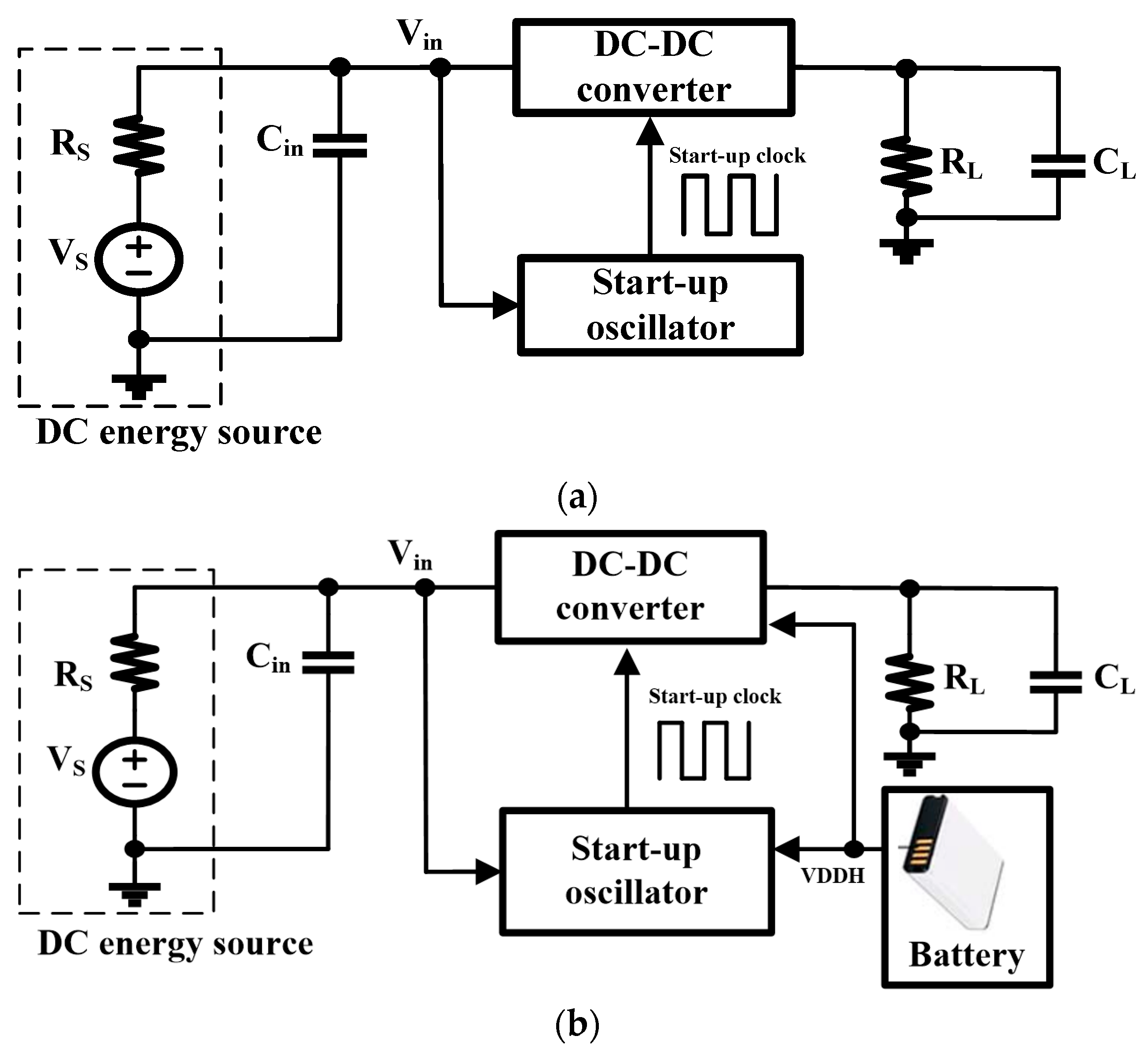
:1. Introduction
2. Literature Review
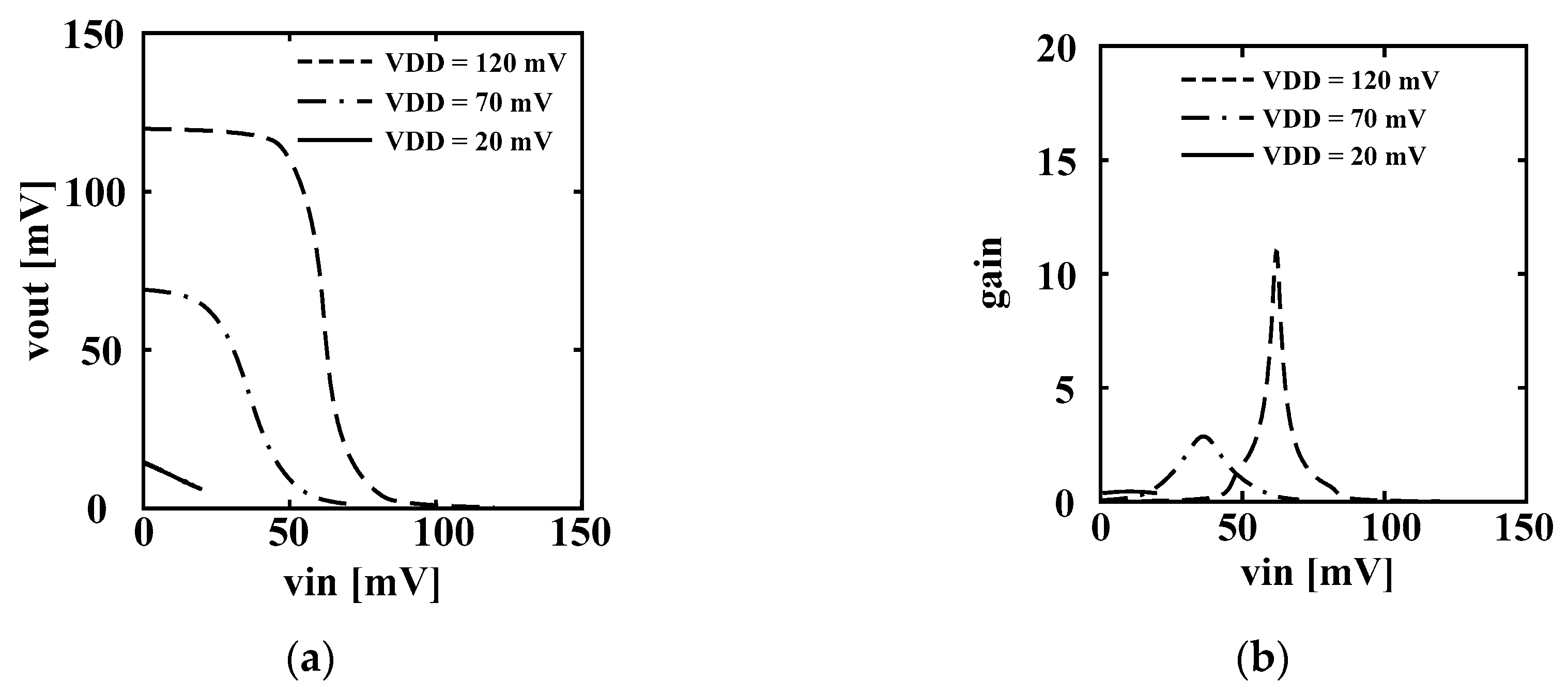
2.1. VTC and DC Gain of Inverters
2.2. Fundamental Limit on Minimum Supply Voltage
2.3. Overview of Low-Voltage Delay Elements for Cold Start-Up Ring Oscillator
3. Proposed Low Voltage Delay Element
4. Layout and Post-Layout Experimental Results
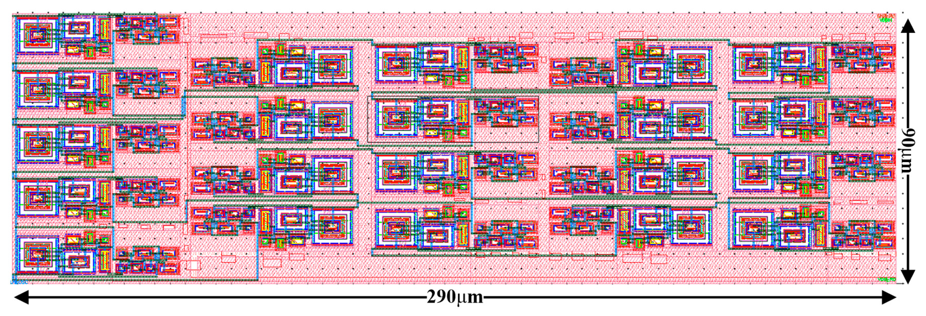
4.1. Layout of Ring Oscillator
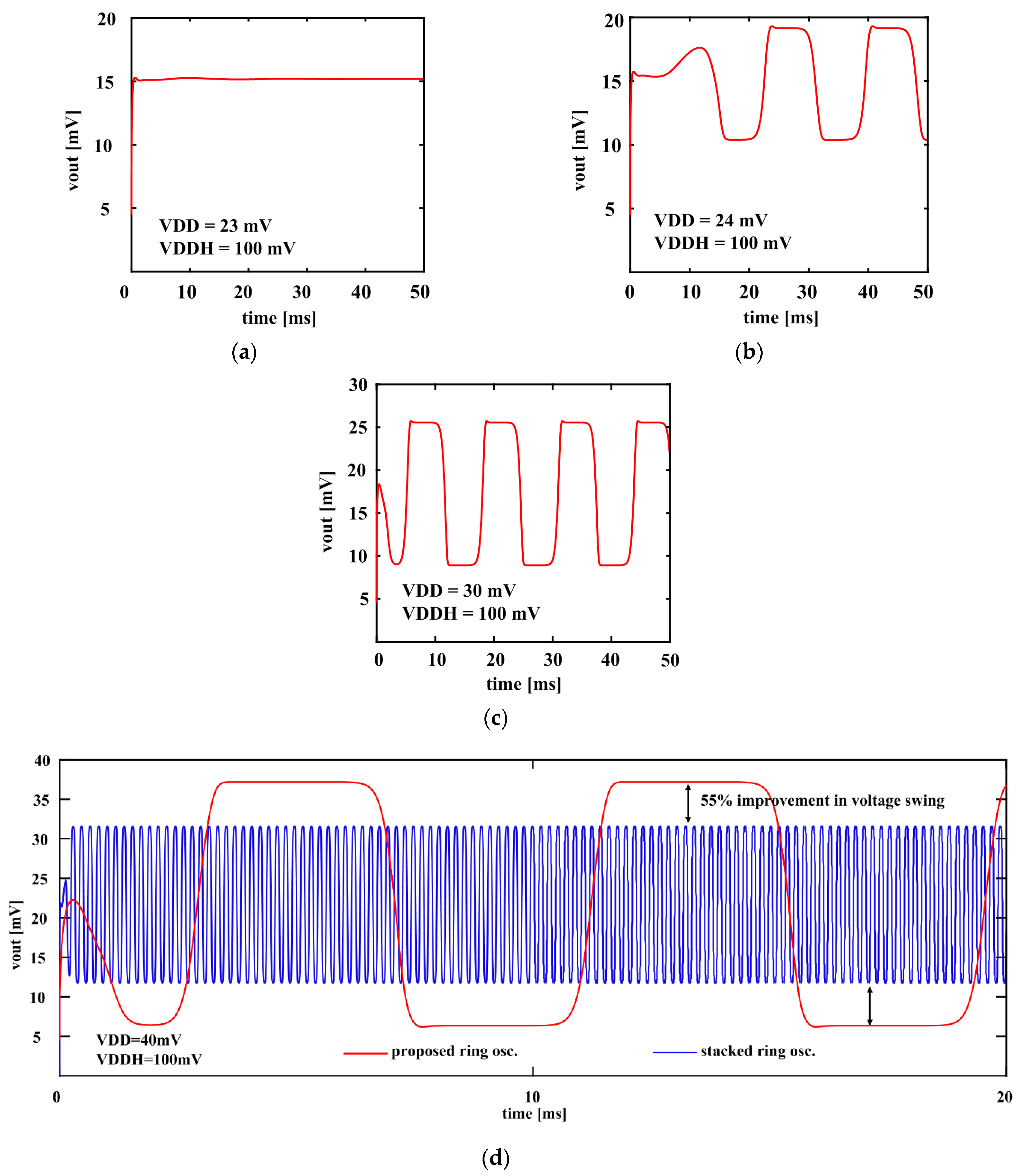
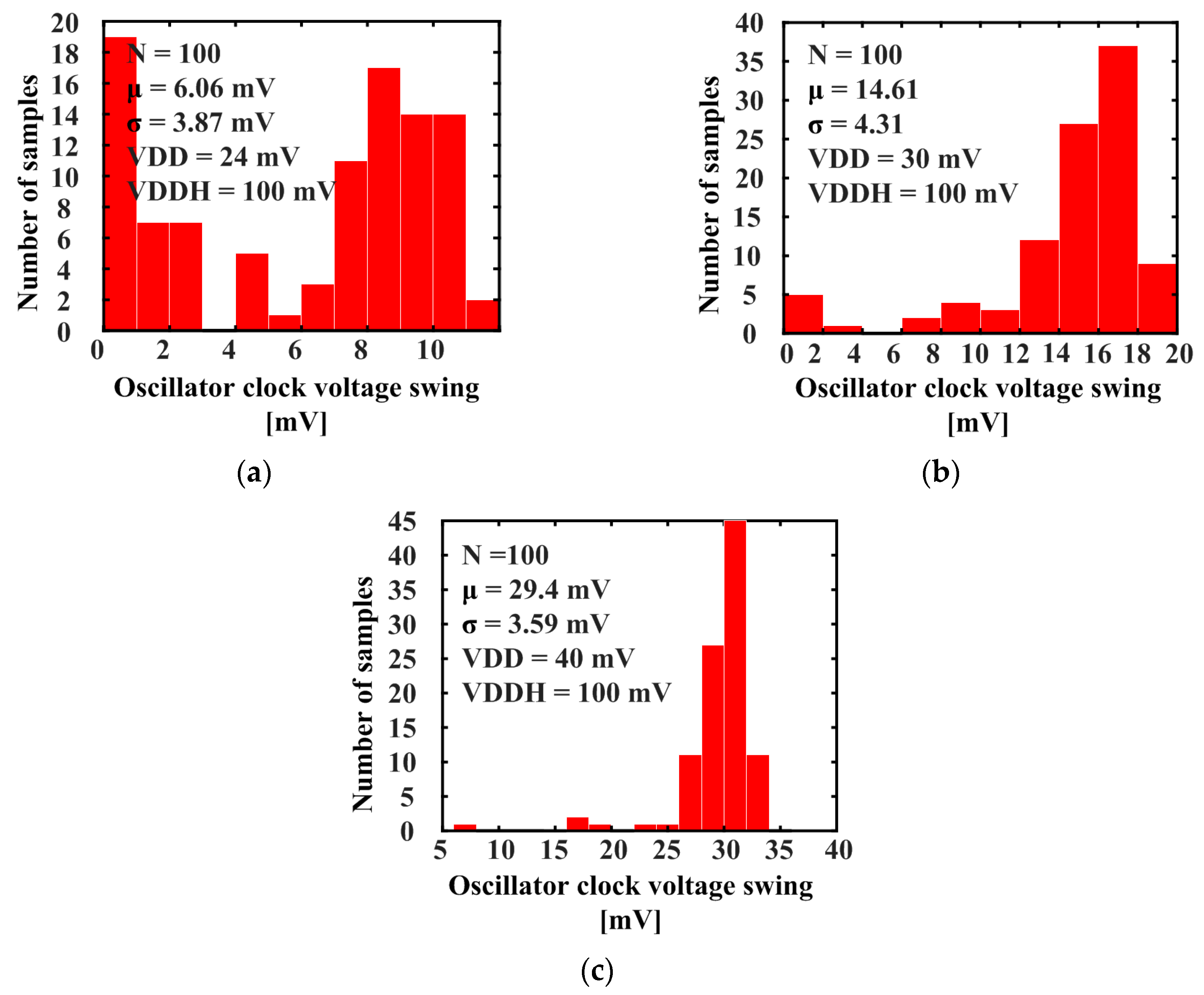
4.2. Post-layout Experimental Results of Proposed Delay Element
4.3. Post-Layout Experimental Result Comparison of Ring Oscillator with Two Different Delay Elements
5. Conclusions
Author Contributions
Funding
Conflicts of Interest
References
- Selvakumar, A.; Zargham, M.; Liscidini, A. Sub-mW current re-use receiver front-end for wireless sensor network applications. IEEE J. Solid State Circuits 2015, 50, 2965–2974. [Google Scholar] [CrossRef]
- Ramadass, Y.K.; Chandrakasan, A.P. A battery-less thermoelectric energy harvesting interface circuit with 35 mV startup voltage. IEEE J. Solid State Circuits 2011, 46, 333–341. [Google Scholar] [CrossRef]
- Im, J.P.; Wang, S.W.; Ryu, S.T. A 40 mV transformer-reuse self-startup boost converter with MPPT control for thermoelectric energy harvesting. IEEE J. Solid State Circuits 2012, 47, 3055–3067. [Google Scholar] [CrossRef]
- Weng, P.S.; Tang, H.Y.; Ku, P.C. 50 mV-input batteryless boost converter for thermal energy harvesting. IEEE J. Solid State Circuits 2013, 48, 1031–1041. [Google Scholar] [CrossRef]
- Chen, P.H.; Ishida, K.; Ikeuchi, K. A 95 mV-startup step-up converter with VTH-tuned oscillator by fixed-charge programming and capacitor pass-on scheme. In Proceedings of the 2011 IEEE International Solid-State Circuits Conference, San Francisco, CA, USA, 20–24 February 2011; pp. 216–218. [Google Scholar]
- Goeppert, J.; Manoli, Y. Fully integrated startup at 70 mV of boost converters for thermoelectric energy harvesting. IEEE J. Solid State Circuits 2016, 51, 1716–1726. [Google Scholar] [CrossRef]
- Dezyani, M.; Ghafoorifard, H.; Sheikhaei, S. A 60 mV input voltage, process tolerant start-up system for thermoelectric energy harvesting. IEEE Trans. Circuits Syst. I Regul. Pap. 2018, 65, 3568–3577. [Google Scholar] [CrossRef]
- Bose, S.; Anand, T.; Johnston, M.L. Fully-integrated 57 mV cold start of a thermoelectric energy harvester using a cross-coupled complementary charge pump. In Proceedings of the 2018 IEEE Custom Integrated Circuits Conference (CICC), San Diego, CA, USA, 8–11 April 2018; pp. 1–4. [Google Scholar]
- Luo, Z.; Zeng, L.; Lau, B. A sub-10 mV power converter with fully integrated self-start, MPPT, and ZCS control for thermoelectric energy harvesting. IEEE Trans. Circuits Syst. I Regul. Pap. 2017, 65, 1744–1757. [Google Scholar] [CrossRef]
- Bose, S.; Johnston, M.L. A stacked-inverter ring oscillator for 50 mV fully-integrated cold-start of energy harvesters. In Proceedings of the 2018 IEEE International Symposium on Circuits and Systems (ISCAS), Florence, Italy, 27–30 May 2018; pp. 1–5. [Google Scholar]
- Bose, S.; Anand, T.; Johnston, M.L. Integrated Cold Start of a Boost Converter at 57 mV Using Cross-Coupled Complementary Charge Pumps and Ultra-Low-Voltage Ring Oscillator. IEEE J. Solid State Circuits 2019, 54, 2867–2878. [Google Scholar] [CrossRef]
- Bose, S.; Anand, T.; Johnston, M.L. A 3.5 mV Input, 82% Peak Efficiency Boost Converter with Loss-Optimized MPPT and 50 mV Integrated Cold-Start for Thermoelectric Energy Harvesting. In Proceedings of the 2019 IEEE Custom Integrated Circuits Conference (CICC), Austin, TX, USA, 14–17 April 2019; pp. 1–4. [Google Scholar]
- Kim, J.; Kim, C. A DC–DC boost converter with variation-tolerant MPPT technique and efficient ZCS circuit for thermoelectric energy harvesting applications. IEEE Trans. Power Electron. 2012, 28, 3827–3833. [Google Scholar] [CrossRef]
- Prabha, R.D.; Rincón-Mora, G.A. 0.18-μm Light-Harvesting Battery-Assisted Charger–Supply CMOS System. IEEE Trans. Power Electron. 2015, 31, 2950–2958. [Google Scholar] [CrossRef]
- Zushuai, X.; Zhiqiang, W.; Jianhui, W. Low voltage delay element with dynamic biasing technique for fully integrated cold-start in DC energy harvesting systems. Int. J. Electron. Commun. 2020, 127, 153416. [Google Scholar]
- Meindl, J.D.; Davis, J.A. The fundamental limit on binary switching energy for terascale integration (TSI). IEEE J. Solid State Circuits 2000, 35, 1515–1516. [Google Scholar] [CrossRef]
- Zhai, B.; Blaauw, D.; Sylvester, D. The limit of dynamic voltage scaling and insomniac dynamic voltage scaling. IEEE Trans. Large Scale Integr. VLSI Syst. 2005, 13, 1239–1252. [Google Scholar] [CrossRef]
- Kim, J.; Mok, P.K.T.; Kim, C. A 0.15 V input energy harvesting charge pump with dynamic body biasing and adaptive dead-time for efficiency improvement. IEEE J. Solid State Circuits 2014, 50, 414–425. [Google Scholar] [CrossRef]
- Radin, R.L.; Sawan, M.; Galup-Montoro, C. A 7.5 mV-Input Boost Converter for Thermal Energy Harvesting with 11 mV Self-Startup. IEEE Trans. Circuits Syst. II Express Br. 2020, 67, 1379–1383. [Google Scholar] [CrossRef]
- Machado, M.B.; Schneider, M.C.; Galup-Montoro, C. On the minimum supply voltage for MOSFET oscillators. IEEE Trans. Circuits Syst. I Regul. Pap. 2013, 61, 347–357. [Google Scholar] [CrossRef]
- Lotze, N.; Manoli, Y. A 62 mV 0.13μm CMOS Standard-Cell-Based Design Technique Using Schmitt-Trigger Logic. IEEE J. Solid State Circuits 2011, 47, 47–60. [Google Scholar] [CrossRef]
- Lotze, N.; Manoli, Y. Ultra-sub-threshold operation of always-on digital circuits for IoT applications by use of Schmitt trigger gates. IEEE Trans. Circuits Syst. I Regul. Pap. 2017, 64, 2920–2933. [Google Scholar] [CrossRef]
- Ferreira, J.V.T.; Galup-Montoro, C. Ultra-low-voltage CMOS ring oscillators. Electron. Lett. 2019, 55, 523–525. [Google Scholar] [CrossRef]
- Siniscalchi, M.; Silveira, F.; Galup-Montoro, C. Ultra-low-voltage CMOS crystal oscillators. IEEE Trans. Circuits Syst. I Regul. Pap. 2020, 67, 1846–1856. [Google Scholar] [CrossRef]
- Kabirpour, S.; Jalali, M. A power-delay and area efficient voltage level shifter based on a reflected-output Wilson current mirror level shifter. IEEE Trans. Circuits Syst. II Express Br. 2020, 67, 250–254. [Google Scholar] [CrossRef]


| Ref. | Process (nm) | Cold Start Voltage (mV) |
|---|---|---|
| [5] | 65 | 95 |
| [6] | 180 | 70 |
| [7] | 180 | 60 |
| [8] | 65 | 68 A/150 B/210 C |
| [9,10,11,12] | 180 | 37 B/57 C |
| [15] | 180 | 36 B |
| Transistor | Width (μm) | Length (μm) | Transistor | Width (μm) | Length (μm) |
|---|---|---|---|---|---|
| M1 | 2.28 | 0.25 | M8 | 0.22 | 0.18 |
| M2 | 1.80 | 0.60 | M9 | 0.22 | 0.18 |
| M3 | 3.80 | 0.25 | M10 | 0.22 | 0.18 |
| M4 | 1.80 | 0.60 | M11 | 0.22 | 0.18 |
| M5 | 0.76 | 0.25 | M12 | 0.22 | 0.18 |
| M6 | 5.58 | 0.60 | M13 | 0.22 | 0.18 |
| M7 | 0.22 | 0.18 | M14 | 0.22 | 0.18 |
| Ref. | Year | Process (nm) | Oscillator Type | Start-Up Technique | Start-Up Voltage (mV) | Off-Chip Components |
|---|---|---|---|---|---|---|
| [2] | 2010 | 350 | Mechanical switch | Mechanical motion | 35 2 | 1C + 1L + 1S |
| [3] | 2012 | 130 | Transformer based | White noise | 40 2 | 1T + 4C + 2D |
| [4] | 2013 | 65 | LC based | LS osc. | 22 1 | 2L + 1C |
| [5] | 2011 | 65 | Ring | Body fixed control | 95 2 | - |
| [6] | 2016 | 180 | Ring | Schmitt trigger ring osc. | 70 2 | - |
| [8] | 2018 | 180 | Ring | Stacked inverter based ring osc. | 57 2 | - |
| [9] | 2018 | 65 | Ring | 150 1 | - | |
| [10] | 2018 | 180 | Ring | 37 1 | - | |
| [15] | 2020 | 180 | Ring | Stacked inverter based ring osc. with body dynamical control | 36 1 | - |
| This work | 2020 | 180 | Ring | VLS assistance ring osc. | 24 1 | - |
© 2020 by the authors. Licensee MDPI, Basel, Switzerland. This article is an open access article distributed under the terms and conditions of the Creative Commons Attribution (CC BY) license (http://creativecommons.org/licenses/by/4.0/).
Share and Cite
Xie, Z.; Wu, Z.; Wu, J. Low Voltage Delay Element with Dynamic Biasing Technique for Fully Integrated Cold-Start in Battery-Assistance DC Energy Harvesting Systems. Appl. Sci. 2020, 10, 6993. https://doi.org/10.3390/app10196993
Xie Z, Wu Z, Wu J. Low Voltage Delay Element with Dynamic Biasing Technique for Fully Integrated Cold-Start in Battery-Assistance DC Energy Harvesting Systems. Applied Sciences. 2020; 10(19):6993. https://doi.org/10.3390/app10196993
Chicago/Turabian StyleXie, Zushuai, Zhiqiang Wu, and Jianhui Wu. 2020. "Low Voltage Delay Element with Dynamic Biasing Technique for Fully Integrated Cold-Start in Battery-Assistance DC Energy Harvesting Systems" Applied Sciences 10, no. 19: 6993. https://doi.org/10.3390/app10196993
APA StyleXie, Z., Wu, Z., & Wu, J. (2020). Low Voltage Delay Element with Dynamic Biasing Technique for Fully Integrated Cold-Start in Battery-Assistance DC Energy Harvesting Systems. Applied Sciences, 10(19), 6993. https://doi.org/10.3390/app10196993