Article

High Selectivity Slot-Coupled Bandpass Filter Using Discriminating Coupling and Source-Load Coupling

School of Electronic and Optical Engineering, Nanjing University of Science and Technology, Nanjing 210094, China
*
Author to whom correspondence should be addressed.
Appl. Sci. 2020, 10(19), 6807; https://doi.org/10.3390/app10196807
Submission received: 15 August 2020 / Revised: 16 September 2020 / Accepted: 17 September 2020 / Published: 28 September 2020
(This article belongs to the Special Issue Passive Planar Microwave Devices )

Abstract

:
A multilayer bandpass filter with high selectivity is proposed in this letter. Discriminating coupling formed by slot-coupled quarter-wavelength and half-wavelength resonators introduces a zero at 3f 0 (f 0 is the center frequency) and the second harmonic is also suppressed due to the quarter-wavelength resonators. Owing to multilayer structure, source-load coupling is introduced to improve selectivity. Then an extra coupled line path is added with the same amplitude as the discriminating coupling path while they are out of phase. Thus signal cancellation produces three extra transmission zeros, with the selectivity and suppression performance further improved. To validate the design, a prototype bandpass filter centered at 2.49 GHz with 3 dB fractional bandwidth of 8.1% is fabricated. Both simulated and measured results are in good agreement and show good performance of the proposed bandpass filter.

1. Introduction

Bandpass filter (BPF) is an essential component in transmitters and receivers. For anti-interference, high performance BPF with sharp selectivity as well as wide stopband is important and necessary. Due to limited and crowded spectrum nowadays, there are more and more challenges in designing such bandpass filters in modern wireless systems.
Traditionally, the selectivity of BPF can be improved by increasing the order at the expense of larger insertion loss. While quasi-elliptic function response can realize the same selectivity with fewer orders and thus quasi-elliptic filter has lower insertion loss with high selectivity [1]. In [2], stub-loaded half-wavelength resonators are electromagnetically coupled to form quasi-elliptic response. In addition to specific response functions, introducing multiple transmission zeros (TZs) near the passband can effectively improve the selectivity [3]. Source-load coupling [4,5] and mixed coupling [6] are both proved to be useful by introducing TZs at sidebands. In [7], capacitive dominant mixed coupling is used to create a lower stopband TZ while the upper stopband selectivity is enhanced by employing parallel source-load coupling. Mixed coupling is also common when designing high selectivity SIW BPFs [8,9,10]. Furthermore, merely several coupled line networks can introduce both transmission zeros and poles. In [11], a high selectivity bandpass filter with 5 zeros and 6 poles is obtained by six pairs of coupled lines. Another way to realize prescribed TZs is synthesis of the coupling matrix to generate the transfer and reflection polynomials for specific class of filter [12,13], and to simplify the computational complexity and eliminate redundancy, synthesis algorithms are invented to extract coupling matrix from zeros and poles [14,15].
In this paper, a multilayer bandpass filter with high selectivity is proposed. The second and third harmonics are eliminated by the quarter-wavelength resonators and discriminating coupling formed by quarter- and half-wavelength resonators respectively, resulting in a wide stopband as well. This discriminating coupling path has same amplitude as an extra coupled line path between feeding ports but they are out of phase. Thus transmission zeros are produced to not only improve the selectivity but also broaden the stopband performance of the proposed BPF. Furthermore, due to multilayer structure, source-load coupling is easily achieved to improve selectivity as well. Theoretical analysis of the proposed BPF is demonstrated in detail and a prototype is fabricated to validate the design. Both simulated and measured results are in good agreement, showing the good performance of the proposed BPF.

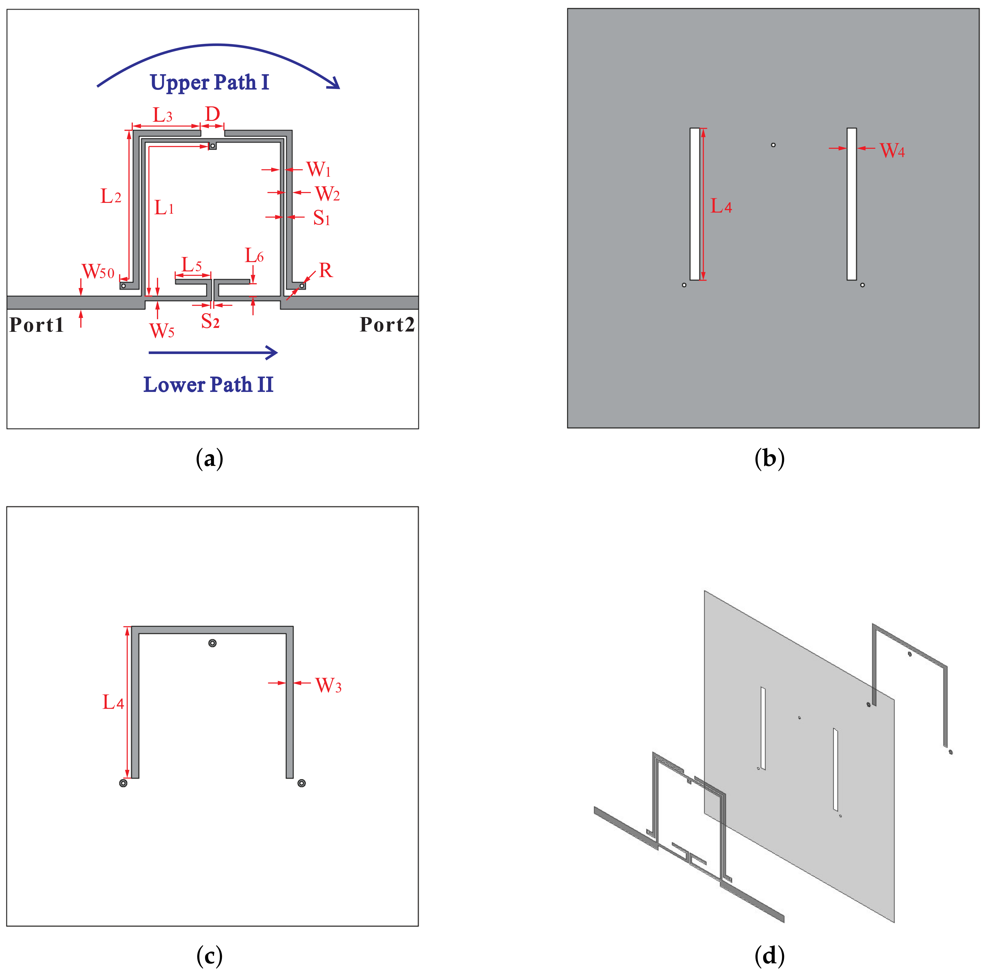
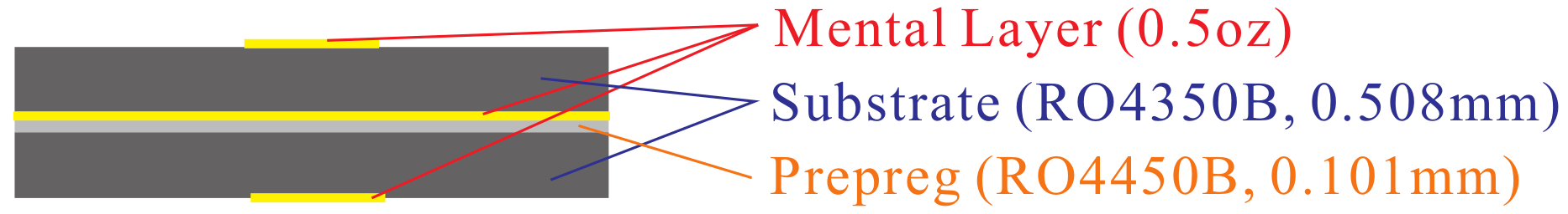
2. Structure and Design of The  BPF

The proposed BPF has two independent paths as is shown in Figure 1. Upper path I is composed of a pair of shorted quarter-wavelength resonators in the top layer and one half-wavelength resonator in the bottom layer, with two rectangular slots etched in the middle ground layer to realize slot-coupling. And this path is coupled to two quarter-wavelength short microstrip lines as exciting structure. Lower path II consists of a stub-loaded anti-parallel coupled line, connecting to the feeding ports in parallel with upper path I. Both of these two paths will be analyzed in detail next.

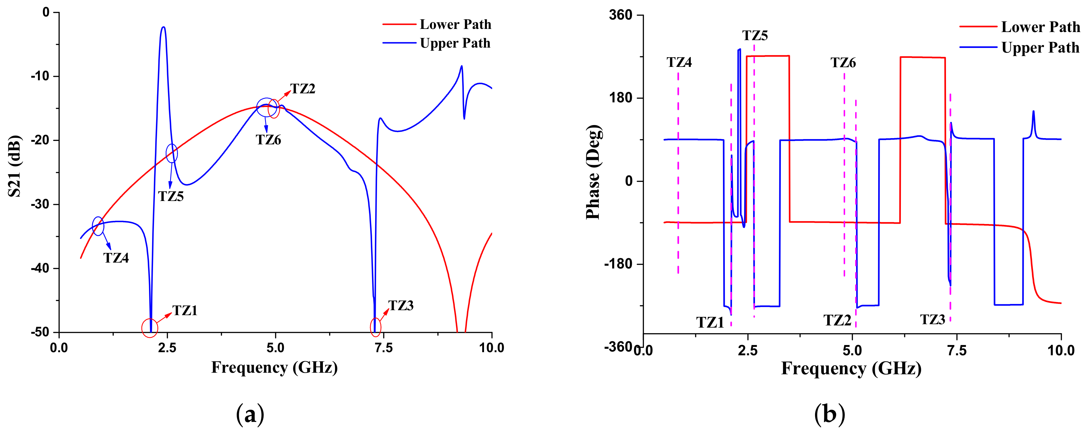
2.1. Analysis of Upper Path I

Figure 2 shows the equivalent circuit of upper path I. The coupling networks consisting of quarter- and half-wavelength resonators are marked as red (T1–T5), (T1+T2 and T4+T5 are quarter-wavelength, T2+T3+T4 is half-wavelength), which are excited by two shorted quarter-wavelength resonators marked as blue (T6) from port 1 and 2, respectively. T2 and T4 are two end-to-end coupled lines with even and odd impedance of Z e 1 and Z o 1 , electric length of θ 2 . Three Microstrip lines T1, T3 and T5 are connected to coupling networks T2 and T4. T1 and T5 are connected to the shorted lines in T2 and T4 with impedance of Z 1 and electric length of θ 1 while T3 is used to connect T2 and T4 with impedance of Z 2 but two times longer than T1 or T5. The total length of T1 and T2 or T4 and T5 is quarter-wavelength ( θ 1 + θ 2 = π / 2 ).
To verify the analysis, we use transfer matrix ABCD which is defined as Equation (1) shows [16]:
V 1 I 1 = A B C D V 2 I 2
For transmission lines with character impedance Z 0 and electrical length θ [16]:
A B C D = c o s θ j Z 0 sin θ j Y 0 sin θ cos θ
Thus the response of the coupling network can be calculated by multiplying the ABCD matrixes as Equation (3).
T = T 1 × T 2 × T 3 × T 4 × T 5
where
T 1 = c o s θ 1 j Z 1 sin θ 1 j Y 1 sin θ 1 cos θ 1 = T 5
T 3 = cos 2 θ 1 j Z 2 sin 2 θ 1 j Y 2 sin 2 θ 1 cos 2 θ 1
T 2 = 1 a b c f a 2 d f a c d b e a b f e c b 2
T 4 = 1 a b d e b 2 c e d b a c f b a e f d a 2
Here a to f in Equation (4) represent formulas related to the dimensions of coupling network T2 and T4 [17] as Equation (5).
a = 1 2 ( cos θ 2 e + cos θ 2 o )
b = 1 2 ( cos θ 2 e cos θ 2 o )
c = j 1 2 ( Z e 1 cos θ 2 e + Z o 1 cos θ 2 o )
d = j 1 2 ( Z e 1 cos θ 2 e Z o 1 cos θ 2 o )
e = j 1 2 ( Y e 1 cos θ 2 e + Y o 1 cos θ 2 o )
f = j 1 2 ( Y e 1 cos θ 2 e Y o 1 cos θ 2 o )
θ 2 e and θ 2 o are the even and odd electric lengths of slot-coupled resonators while Z e 1 , Z o 1 and Y e 1 , Y o 1 are the impedances and admittances. All of these parameters can be obtained using quasi-static analysis [18].
It is noteworthy that if the length of the slots θ 2 is two-third of quarter-wavelength, discriminating coupling is formed. According to [19], a zero at 3f 0 will appear when discriminating coupling occurs, because the voltage distribution is odd on one line and even on the other, leading to null coupling coefficient. Figure 2 shows the simulated result using MATLAB to validate the performance of discriminating. Blue line in Figure 2 demonstrates the simulated result of coupling networks including the connecting microstrip lines (T1-T5) and it is seen that there are two modes and one zero. Thus this line validates that discriminating coupling is effective to introduce a transmission zero at 3f 0 in this design. However, the second mode is located at around 2f 0 because coupling network T2,T4 and microstrip line section M3 realize a half-wavelength resonator in the bottom layer as is clearly shown in Figure 1. To suppress the harmonic caused by half-wavelength resonator, quarter-wavelength shorted coupled lines (M6) is used as feeding lines to introduce another zero at 2f 0 . The red line in Figure 2 proves the function of M6.
Finally the black line in Figure 2 gives the MATLAB simulated result of the whole structure including T1-T6. It shows that the second and third harmonics are suppressed by zeros introduced by discriminating coupling and quarter-wavelength resonators, validating the theory and design very well. Also due to multilayer structure, it is easy to introduce source-load coupling using the short pins of M6 as is shown in the top layer of Figure 1 . Thus a zero located at lower side-band appears and improves the selectivity. HFSS simulated results will validate the design in the next subsection.

2.2. Analysis of Lower Path Ii

The lower path II consists of a stub-loaded anti-parallel coupling section connected by microstrip lines, as is shown in Figure 3. Here the impedance and electric length of connecting microstrip lines are Z 3 and θ 3 . The anti-parallel coupled line has even and odd impedance of Z e 2 and Z o 2 and the electric length of θ 3 with loaded stubs of Z 4 and θ 4 . Formula Equation (6) gives the ABCD matrix of lower path II.
T = cos θ 3 j Z 3 sin θ 3 j Y 3 sin θ 3 cos θ 1 A c B c C c D c cos θ 3 j Z 3 sin θ 3 j Y 3 sin θ 3 cos θ 1
A c , B c , C c and D c in Equation (6) are the ABCD matrix’s elements of the stub-loaded anti-parallel coupled line. The method to calculate these elements is same as the one used for coupling networks T2 or T4 [17] as Equation (7).
A c = 1 G [ ( c + a Z s ) ( a + e Z s ) ( d + b Z s ) ( b + f Z s ) ]
B c = 1 G [ ( c + a Z s ) ( c + a Z s ) ( d + b Z s ) ( d + b Z s ) ]
C c = 1 G [ ( a + e Z s ) ( a + e Z s ) ( b + f Z s ) ( b + f Z s ) ]
D c = 1 G [ ( a + e Z s ) ( c + a Z s ) ( b + f Z s ) ( d + b Z s ) ]
where
G = ( d + b Z s ) ( a + e Z s ) ( b + f Z s ) ( c + a Z s )
and
Z s = j Z 4 c o t θ 4
Similarly, a to f in Equation (7) and Equation (8) are same as Equation (5) but the even and odd parameters are replaced by θ 5 e , θ 5 o , Z e 2 , Z o 2 , Y e 2 and Y o 2 . Formula Equation (9) is the input impedance of the open stubs.
MATLAB can also be used to calculate the response of combined upper and lower path. However, the formulas will be very complicated and the simulated result will not be clear enough to demonstrate the function of lower path II. Thus full-wave simulation software Ansys HFSS 19 is used. Blue line in Figure 4 shows the HFSS simulated results of upper path I while the red line gives the ones of lower path II. As is shown in Figure 4, the upper path I has bandpass response with the second and third harmonics suppressed by TZ2 and TZ3, and another transmission zero TZ1 located at lower sideband is introduced by inductive source-load coupling as is mentioned in the last subsection. It can also be seen that the response of lower path II has same amplitude as upper path I in some frequencies but at the same time they are out of phase. So in these frequencies, transmission zeros will appear because of signal cancellation. In this design, three extra transmission zeros TZ4, TZ5 and TZ6 are introduced due to signal cancellation. TZ5 located at upper sideband is used to improve the selectivity while the lower and upper stopband is improved by TZ4 and TZ6. However, TZ2 and TZ6 are both at around 2f 0 . So overall, there are five TZs used to improve selectivity and out-of-band suppression performance.

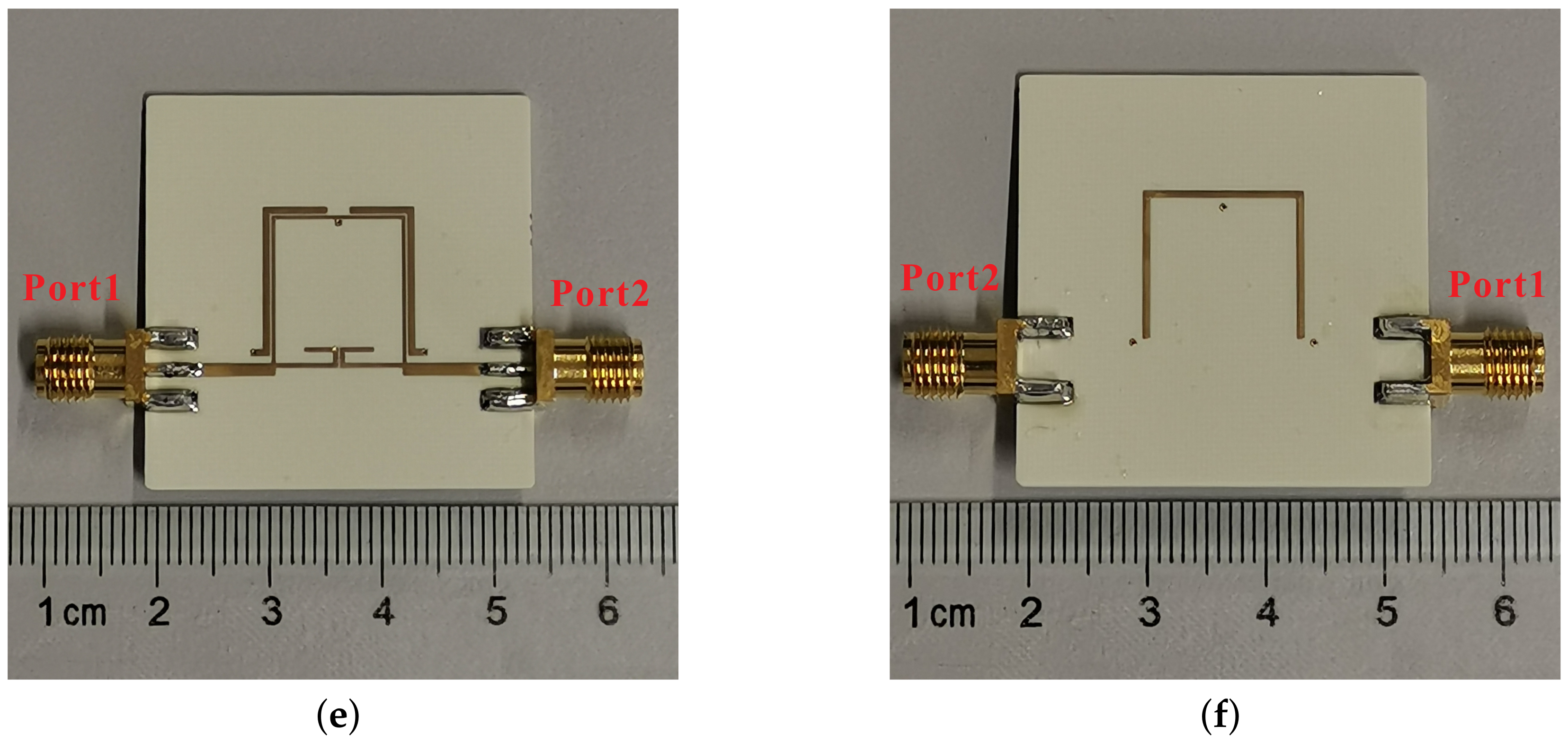
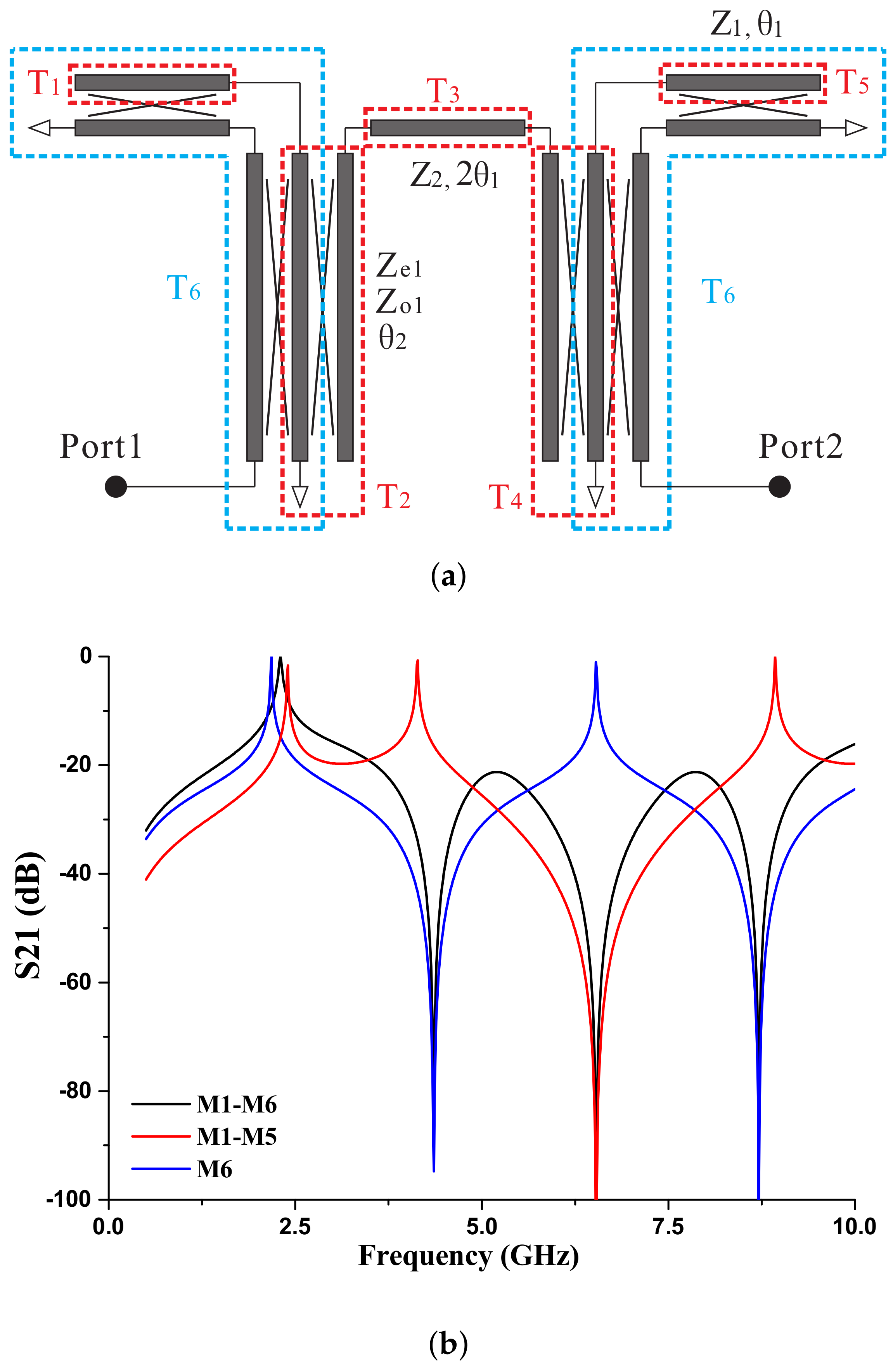
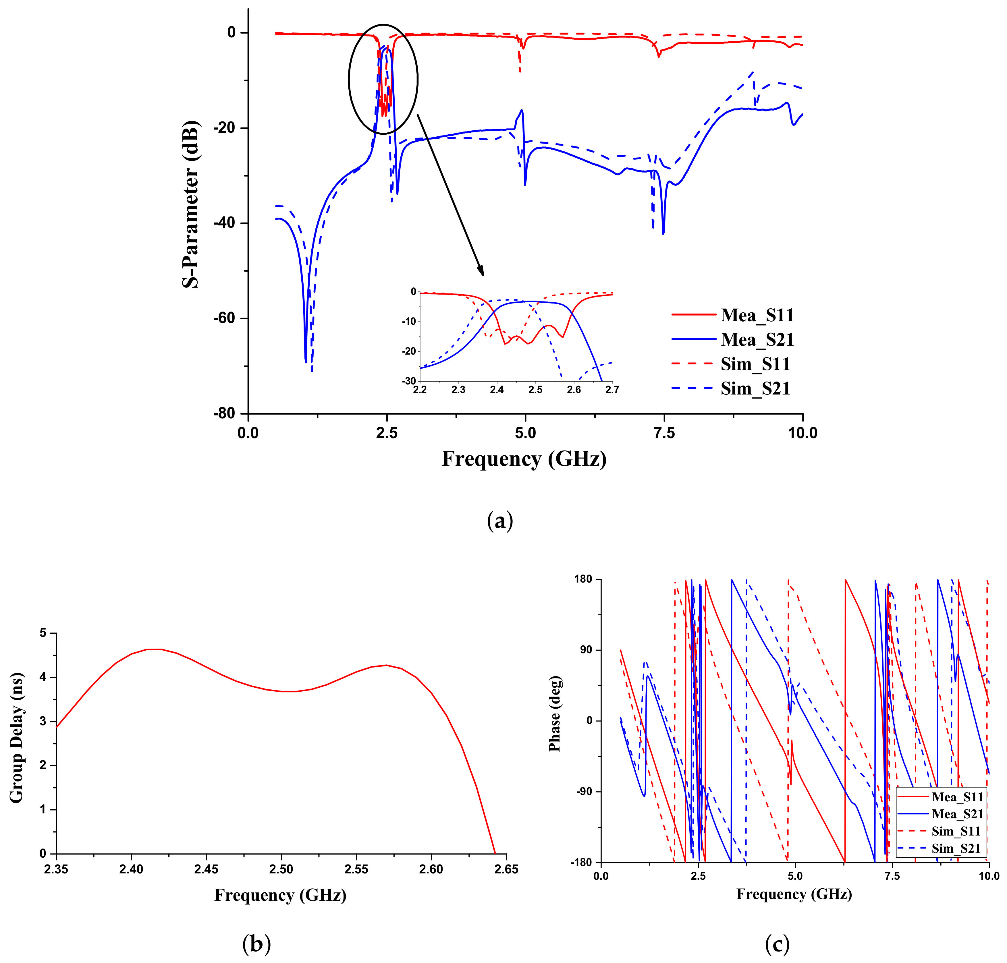
3. Simulated and Measured Results

As shown in Figure 5, the proposed BPF is designed on two RO4350B substrate with relative permittivity of 3.66 and thickness of 0.508 mm. A 0.1 mm RO4450B prepreg is used as paste layer and so the total height of the PCB is 1.116 mm (0.508 + 0.1 + 0.508). The final parameters are: W 1 = 0.3 , W 2 = 0.5 , W 3 = 0.6 , W 4 = 0.8 , W 5 = 0.4 , L 1 = 18.2 , L 2 = 13.8 , L 3 = 5.7 , L 4 = 12.7 , L 5 = 3 , L 6 = 1 , D = 2 , S 1 = S 2 = 0.2 , R = 0.15 , W 50 = 1.1 (unit: mm). To validate the design, a prototype is fabricated and measured using Keysigth ENA network analyser E5671C. The photograph of the proposed bandpass filter is shown in Figure 1.
Figure 6 illustrates the simulated and measured responses. The measured 3 dB bandwidth is from 2.39 GHz to 2.59 GHz (8.1%) centered at 2.49 GHz with return loss better than −12 dB within the passband. Due to mechanical fabrication error and permittivity difference between simulation and production, the center frequency is a little higher for the measurement results. Also the insertion loss is 3.1 dB, larger than simulated one due to 0.6 dB SMA connector loss. The positions of 5 TZs are in agreement with the simulated ones with a little shift. The depicted discrepancies could be from the fabrication tolerance in the etching process. Due to these 5 TZs, the lower sideband selectivity of the proposed BPF is calculated by 3 dB and 20 dB amplitude response with respect to its frequency point:
S e l e c t i v i t y l o w e r s i d e b a n d = | 3 20 f 3 f 20 | = 17 2.39 2.3 = 188.8 dB / GHz
and the upper sideband selectivity:
S e l e c t i v i t y u p p e r s i d e b a n d = | 3 20 f 3 f 20 | = 17 2.65 2.59 = 288.3 dB / GHz
so that the shape factor is BW 20 /BW 3 = 1.75 (BW represents bandwidth). And −15 dB suppression is from 2.64 to 8.84 GHz. The overall size is 0.2 λ g × 0.22 λ g ( λ g is the wavelength at center frequency). Table 1 tabulates the performance comparisons with some previous works. Here CF represents the center frequency of the filter, and FBW is the fractional bandwidth which is calculated by passband (3 dB bandwidth) divide center frequency BW 3 d B / f 0 , and N is the number of TZs, and metal layers are the number of metal used to form the filter. TZ@sideband is the frequency of sideband transmission zeros divide center frequency f s i d e b a n d T Z / f 0 .

4. Conclusions

A multilayer bandpass filter with high selectivity and wide stopband is proposed in this letter. TZs introduced by anti-parallel coupling network as well as discriminating coulpling between quarter- and half-wavelength resonators improve the selectivity and out-of-band suppression of the BPF. To verify the design, a prototype BPF is fabricated centered at 2.49 GHz. Both simulated and measured results manifest the performance with good selectivity and extended stopband. With these features, The proposed BPF is attractive in modern wireless system.

Author Contributions

Conceptualization, J.C. and H.C.; methodology, J.C.; software, H.C.; validation, J.C., H.C.and R.Z.; formal analysis, J.C.; investigation, H.C.; resources, R.Z.; data curation, J.C.; Writing—Original draft preparation, H.C.; Writing—Review and editing, R.Z.; funding acquisition, J.C. All authors have read and agreed to the published version of the manuscript.

Funding

This work has been supported by National Natural Science Foundation of China 62001232, 61971224 and Jiangsu Provincial Natural Science Foundation under Grants Nos. BK20180457.

Conflicts of Interest

The authors declare no conflict of interest.

References

  1. Chen, C.J. A Coupled-Line Coupling Structure for the Design of Quasi-Elliptic Bandpass Filters. IEEE Trans. Microw. Theory Tech. 2018, 66, 1921–1925. [Google Scholar] [CrossRef]
  2. Virdee, B.S.; Riaz, M.; Shukla, P.; Onadim, M.; Ouazzane, K. Wideband microstrip quasi-elliptic function bandpass filter with high out-of-band rejection. Microw. Opt. Technol. Lett. 2019, 61, 1993–1998. [Google Scholar] [CrossRef]
  3. Kim, P.; Chaudhary, G.; Jeong, Y. Wide-stopband and high selectivity step impedance resonator bandpass filter using T-network and antiparallel coupled line. IET Microw. Antennas Propag. 2019, 13, 1916–1920. [Google Scholar] [CrossRef]
  4. Deng, H.W.; Liu, F.; Xu, T.; Sun, L.; Xue, Y.F. Compact and high selectivity dual-mode microstrip BPF with frequency-dependent source-load coupling. Electron. Lett. 2018, 54, 219–221. [Google Scholar] [CrossRef]
  5. Peng, B.; Li, S.; Zhu, J.; Zhang, Q.; Deng, L.; Zeng, Q.; Gao, Y. Wideband Bandpass Filter with High Selectivity Based on Dual-Mode DGS Resonator. Microw. Opt. Technol. Lett. 2016, 58, 2300–2303. [Google Scholar] [CrossRef]
  6. Killamsetty, V.S.; Mukherjee, B. Compact Selective Bandpass Filter With Wide Stopband for TETRA Band Applications. IEEE Trans. Compon. Packag. Manuf. Technol. 2018, 8, 653–659. [Google Scholar] [CrossRef]
  7. Anwar, M.S.; Cao, Q.; Burney, S.A. High selectivity quarter-wavelength resonator bandpass filter utilizing source-load coupling. Microw. Opt. Technol. Lett. 2020, 62, 1176–1182. [Google Scholar] [CrossRef]
  8. Saghati, A.P.; Saghati, A.P.; Entesari, K. Ultra-Miniature SIW Cavity Resonators and Filters. IEEE Trans. Microw. Theory Tech. 2015, 63, 4329–4340. [Google Scholar] [CrossRef]
  9. He, Z.; You, C.J.; Leng, S.; Li, X.; Huang, Y.M. Compact Bandpass Filter with High Selectivity Using Quarter-Mode Substrate Integrated Waveguide and Coplanar Waveguide. IEEE Microw. Wirel. Compon. Lett. 2017, 27, 809–811. [Google Scholar] [CrossRef]
  10. Liu, Q.; Zhou, D.; Shi, J.; Hu, T. High-selective triple-mode SIW bandpass filter using higher-order resonant modes. Electron. Lett. 2020, 56, 37–39. [Google Scholar] [CrossRef]
  11. Zhang, F.; Xu, K.D. High-selectivity bandpass filter using six pairs of quarter-wavelength coupled lines. Electron. Lett. 2019, 55, 544–546. [Google Scholar] [CrossRef]
  12. Cameron, R.J. Advanced Coupling Matrix Synthesis Techniques for Microwave Filters. IEEE Trans. Microw. Theory Tech. 2003, 51, 1–10. [Google Scholar] [CrossRef]
  13. Muller, A.A.; Moldoveanu, A.; Asavei, V.; Sanabria-Codesal, E.; Favennec, J.F. Lossy coupling matrix filter synthesis based on hyperbolic reflections. In Proceedings of the IEEE MTT-S International Microwave Symposium (IMS), San Francisco, CA, USA, 22–27 May 2016. [Google Scholar]
  14. Muller, A.A.; Sanabria-Codesal, E.; Lucyszyn, S. Computational Cost Reduction for N+2 Order Coupling Matrix Synthesis Based on Desnanot-Jacobi Identity. IEEE Access 2016, 4, 10042–10050. [Google Scholar] [CrossRef]
  15. Snyder, R.V.; Mortazawi, A.; Hunter, I.; Bastioli, S.; Macchiarella, G.; Wu, K. Present and Future Trends in Filters and Multiplexers. IEEE Trans. Microw. Theory Tech. 2015, 63, 3324–3360. [Google Scholar] [CrossRef]
  16. Pozar, D.M. THE TRANSMISSION (ABCD) MATRIX. In Microwave Engineering; John Wiley & Sons, Inc.: Hoboken, NJ, USA, 2011; pp. 188–194. [Google Scholar]
  17. Zysman, G.I.; Johnson, A.K. Coupled transmission line networks in an inhomogeneous dielectric medium. IEEE Trans. Microw. Theory Tech. 1969, 17, 753–759. [Google Scholar] [CrossRef]
  18. Wong, M.F.; Hanna, V.F.; Picon, O.; Baudrand, H. Analysis and design of slot-coupled directional couplers between double-sided substrate microstrip lines. IEEE Trans. Microw. Theory Tech. 1991, 29, 2123–2129. [Google Scholar] [CrossRef]
  19. Li, Y.C.; Zhang, X.Y.; Xue, Q.; Baudrand, H. Bandpass Filter Using Discriminating Coupling for Extended Out-of-Band Suppression. IEEE Microw. Wirel. Compon. Lett. 2010, 20, 369–371. [Google Scholar] [CrossRef]
Figure 1. Configuration of the proposed bandpass filter (BPF) (a) Top layer. (b) Middle layer. (c) Bottom layer. (d) 3D view. (e) Front view of the proposed BPF. (f) Bottom view of the proposed BPF
Applsci 10 06807 g001aApplsci 10 06807 g001b
Figure 2. Equivalent circuit and MATLAB simulated results of resonators in upper path I. (a) Equivalent circuit of different sections in upper path I. (b) MATLAB simulated results of different sections in upper path I.
Applsci 10 06807 g002
Figure 3. Equivalent circuit of anti-parallel coupling network in lower path II.
Applsci 10 06807 g003
Figure 4. HFSS Simulated results of lower path (red line) and upper path (blue line). (a) Amplitude of S21 (dB). (b) Phase of S21 (deg)
Applsci 10 06807 g004
Figure 5. Laminate layer definition of the fabricated PCB.
Applsci 10 06807 g005
Figure 6. Simulated and measured results of the proposed BPF (solid lines: measured results; dash lines: simulated results) (a) Simulated and measured amplitude of S parameters (dB). (b) Measured group delay (ns). (c) Simulated and measured phase of S parameters (deg).
Applsci 10 06807 g006
Table 1. Performance Comparisons with previous works
RefCF ( GHz )FBW (%)NTZ@SizebandSize ( λ g * λ g )Mental Layers
[1]21020.85, 1.150.79 × 0.061
[4]2.43.530.83, 1.08-1
[7]2.753.640.89, 1.160.18×0.291
[9]8.71630.99, 1.160.29 × 0.571
[10]13.533.930.97, 1.040.84 × 0.841
This work2.488.150.84, 1.080.20 × 0.223

