Fabrication and Characterization of Biplasmonic Substrates Obtained by Picosecond Laser Pulses

 , ,
, , 
Abstract
Featured Application
Abstract
1. Introduction
2. Materials and Methods
2.1. Materials
2.2. Methods
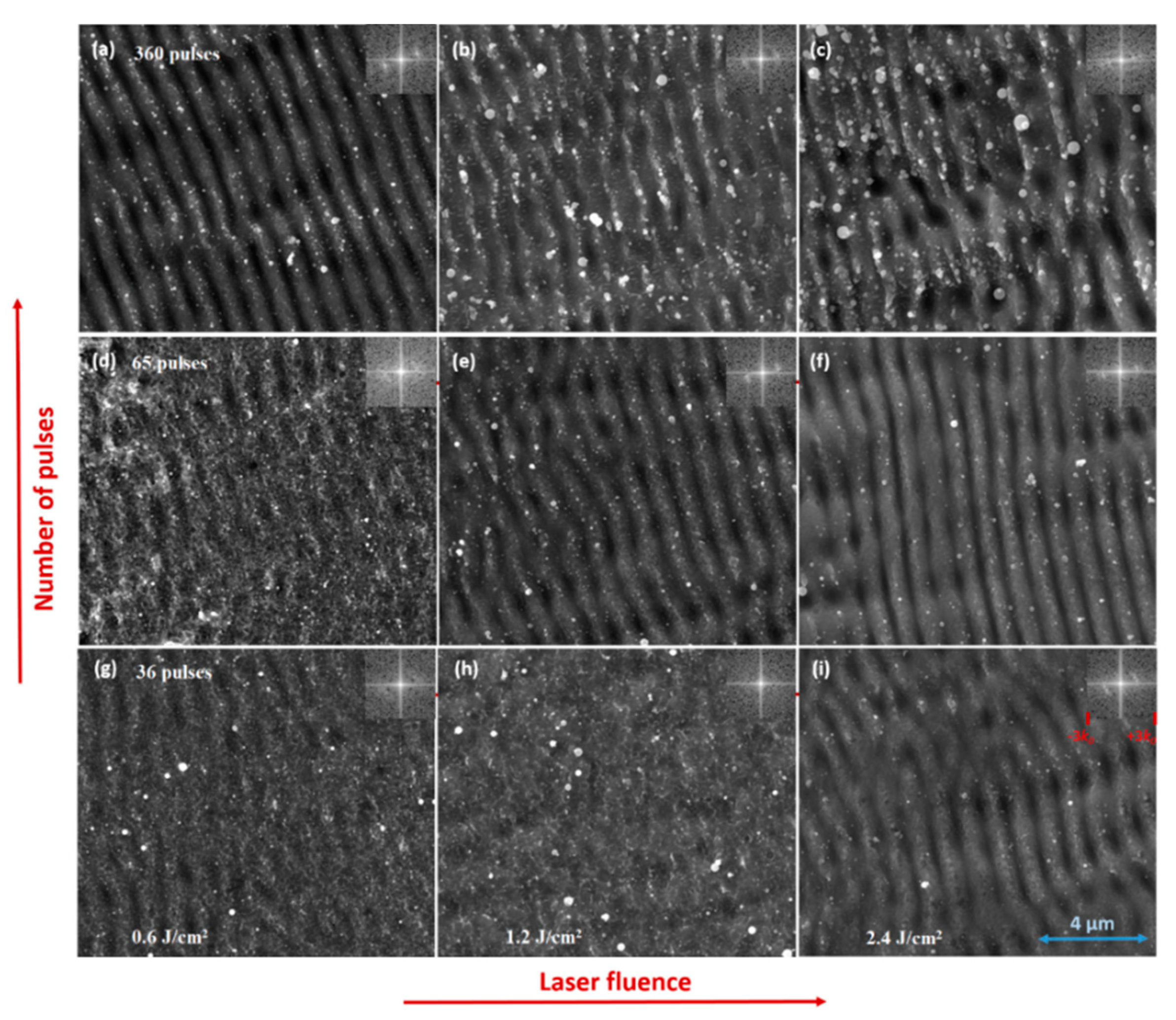
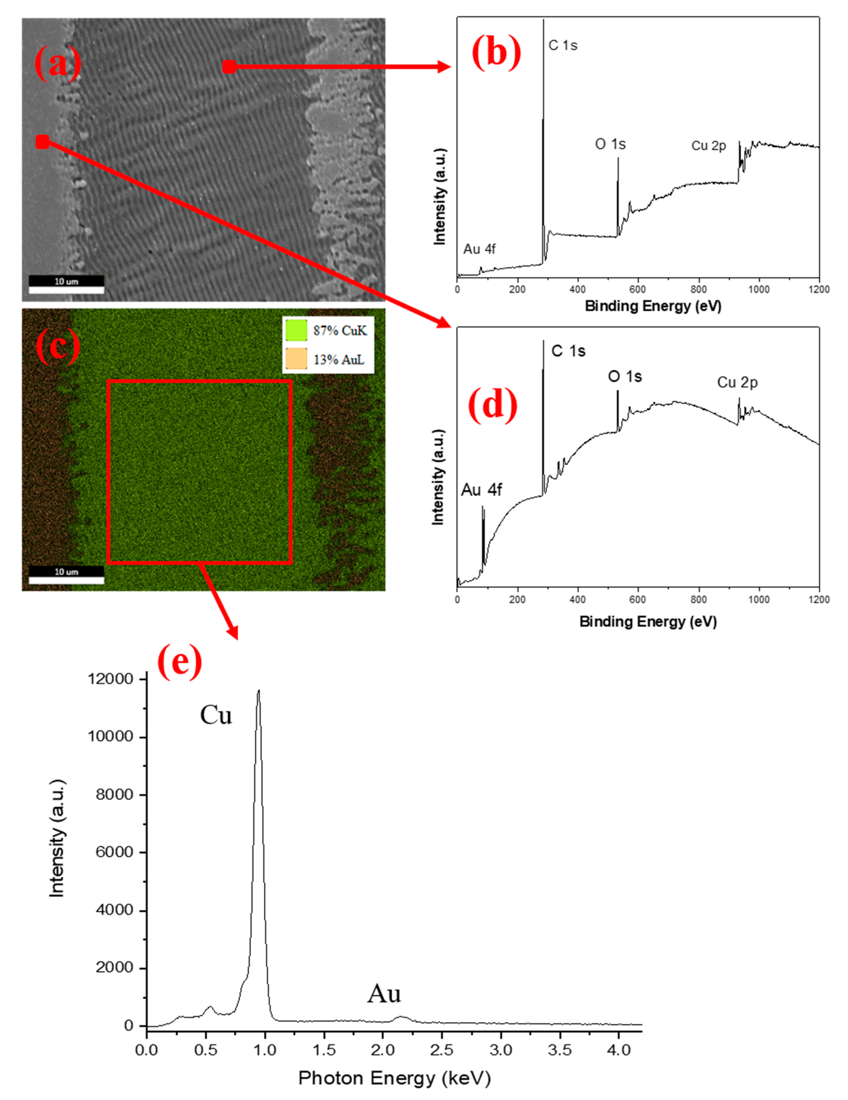
3. Results
4. Conclusions
Author Contributions
Funding
Acknowledgments
Conflicts of Interest
References
- Amer, M.S.; Dosser, L.; LeClair, S.; Maguire, J.F. Induced stresses and structural changes in silicon wafers as a result of laser micro-machining. Appl. Surf. Sci. 2002, 187, 291–296. [Google Scholar] [CrossRef]
- Sugioka, K.; Cheng, Y. Ultrafast lasers—Reliable tools for advanced materials processing. Light Sci. Appl. 2014, 3, e149. [Google Scholar] [CrossRef]
- Alan, C.; Patanjali, K. Chemical Society Reviews: Surface-enhanced Raman Scattering. Phys. Today 1998, 27, 241–250. [Google Scholar]
- Srinoi, P.; Chen, Y.-T.; Vittur, V.; Marquez, M.; Lee, T.; Srinoi, P.; Chen, Y.-T.; Vittur, V.; Marquez, M.D.; Lee, T.R. Bimetallic Nanoparticles: Enhanced Magnetic and Optical Properties for Emerging Biological Applications. Appl. Sci. 2018, 8, 1106. [Google Scholar] [CrossRef]
- Keren, S.; Zavaleta, C.; Cheng, Z.; De La Zerda, A.; Gheysens, O.; Gambhir, S.S.; Phelps, M.E. Noninvasive molecular imaging of small living subjects using Raman spectroscopy. Proc. Natl. Acad. Sci. USA 2008, 105, 5844–5849. [Google Scholar] [CrossRef]
- Wang, Q.; Zhang, C.; Gong, T.; Kong, W.; Yue, W.; Chen, W.; Xie, Z.; Su, Y.; Li, L. Large-scale diamond silver nanoparticle arrays as uniform and sensitive SERS substrates fabricated by surface plasmon lithography technology. Opt. Commun. 2019, 444, 56–62. [Google Scholar] [CrossRef]
- Kosuda, K.M.; Bingham, J.M.; Wustholz, K.L.; Van Duyne, R.P. Nanostructures and Surface-Enhanced Raman Spectroscopy. In Comprehensive Nanoscience and Technology; Elsevier: Evanston, IL, USA; Northwestern University: Evanston, IL, USA, 2010; Volume 1, ISBN 9780123743909. [Google Scholar]
- Šubr, M.; Petr, M.; Kylián, O.; Štěpánek, J.; Veis, M.; Procházka, M. Anisotropic Optical Response of Silver Nanorod Arrays: Surface Enhanced Raman Scattering Polarization and Angular Dependences Confronted with Ellipsometric Parameters. Sci. Rep. 2017, 7, 4293. [Google Scholar] [CrossRef]
- Liu, D.; Wang, Q.; Hu, J. Fabrication and characterization of highly ordered Au nanocone array-patterned glass with enhanced SERS and hydrophobicity. Appl. Surf. Sci. 2015, 356, 364–369. [Google Scholar] [CrossRef]
- Yu, Q.; Guan, P.; Qin, D.; Golden, G.; Wallace, P.M. Inverted size-dependence of surface-enhanced Raman scattering on gold nanohole and nanodisk arrays. Nano Lett. 2008, 8, 1923–1928. [Google Scholar] [CrossRef]
- Schmidl, G.; Jia, G.; Gawlik, A.; Kreusch, J.; Schmidl, F.; Dellith, J.; Dathe, A.; Lin, Z.H.; Huang, J.S.; Plentz, J. Fabrication of self-assembled spherical Gold Particles by pulsed UV Laser Treatment. Sci. Rep. 2018, 8, 11283. [Google Scholar] [CrossRef]
- Gkogkou, D.; Schreiber, B.; Shaykhutdinov, T.; Ly, H.K.; Kuhlmann, U.; Gernert, U.; Facsko, S.; Hildebrandt, P.; Esser, N.; Hinrichs, K.; et al. Polarization- and Wavelength-Dependent Surface-Enhanced Raman Spectroscopy Using Optically Anisotropic Rippled Substrates for Sensing. ACS Sens. 2016, 1, 318–323. [Google Scholar] [CrossRef]
- Abu Hatab, N.A.; Oran, J.M.; Sepaniak, M.J. Surface-enhanced Raman spectroscopy substrates created via electron beam lithography and nanotransfer printing. ACS Nano 2008, 2, 377–385. [Google Scholar] [CrossRef] [PubMed]
- Byram, C.; Moram, S.S.B.; Soma, V.R. Surface-enhanced Raman scattering studies of gold-coated ripple-like nanostructures on iron substrate achieved by femtosecond laser irradiation in water. J. Raman Spectrosc. 2019, 50, 1103–1113. [Google Scholar] [CrossRef]
- Byram, C.; Moram, S.S.B.; Soma, V.R. SERS based detection of multiple analytes from dye/explosive mixtures using picosecond laser fabricated gold nanoparticles and nanostructures. Analyst 2019, 144, 2327–2336. [Google Scholar] [CrossRef]
- Lu, L.; Zhang, J.; Jiao, L.; Guan, Y. Large-scale fabrication of nanostructure on bio-metallic substrate for surface enhanced raman and fluorescence scattering. Nanomaterials 2019, 9, 916. [Google Scholar] [CrossRef]
- Buividas, R.; Stoddart, P.R.; Juodkazis, S. Laser fabricated ripple substrates for surface-enhanced Raman scattering. Ann. Phys. 2012, 524, L5–L10. [Google Scholar] [CrossRef]
- Huang, M.; Zhao, F.; Cheng, Y.; Xu, N.; Xu, Z. Origin of laser-induced near-subwavelength ripples: Interference between surface plasmons and incident laser. ACS Nano 2009, 3, 4062–4070. [Google Scholar] [CrossRef]
- Ranno, L.; Forno, S.D.; Lischner, J. Computational design of bimetallic core-shell nanoparticles for hot-carrier photocatalysis. NPJ Comput. Mater. 2018, 4, 31. [Google Scholar] [CrossRef]
- Domke, M.; Nobile, L.; Rapp, S.; Eiselen, S.; Sotrop, J.; Huber, H.P.; Schmidt, M. Understanding thin film laser ablation: The role of the effective penetration depth and the film thickness. Phys. Procedia 2014, 56, 1007–1014. [Google Scholar] [CrossRef]
- Li, W.-H.; Li, X.-Y.; Yu, N.-T. Surface-enhanced resonance hyper-Raman scattering and surface-enhanced resonance Raman scattering of dyes adsorbed on silver electrode and silver colloid: A comparison study. Chem. Phys. Lett. 1999, 312, 28–36. [Google Scholar] [CrossRef]
- Li, G.; Li, H.; Mo, Y.; Huang, X.; Chen, L. Surface enhanced resonance Raman spectroscopy of rhodamine 6G adsorbed on silver electrode in lithium batteries. Chem. Phys. Lett. 2000, 330, 249–254. [Google Scholar] [CrossRef]
- Baia, M.; Baia, L.; Astilean, S. Gold nanostructured films deposited on polystyrene colloidal crystal templates for surface-enhanced Raman spectroscopy. Chem. Phys. Lett. 2005, 404, 3–8. [Google Scholar] [CrossRef]
- Watanabe, H.; Hayazawa, N.; Inouye, Y.; Kawata, S. DFT Vibrational Calculations of Rhodamine 6G Adsorbed on Silver: Analysis of Tip-Enhanced Raman Spectroscopy. J. Phys. Chem. B 2005, 109, 5012–5020. [Google Scholar] [CrossRef] [PubMed]
- Soejima, T.; Ohkubo, Y. Baseline Setting Method. Japan Patent 4966337B2, 4 July 2012. [Google Scholar]
- Silmeco—SERS Substrates. Available online: https://shop.silmeco.com/ (accessed on 21 March 2019).
- Schmidt, M.S.; Hübner, J.; Boisen, A. Large area fabrication of leaning silicon nanopillars for Surface Enhanced Raman Spectroscopy. Adv. Mater. 2012, 24, 11–18. [Google Scholar] [CrossRef] [PubMed]


© 2020 by the authors. Licensee MDPI, Basel, Switzerland. This article is an open access article distributed under the terms and conditions of the Creative Commons Attribution (CC BY) license (http://creativecommons.org/licenses/by/4.0/).
Share and Cite
Stochioiu, A.; Luculescu, C.; Paun, I.A.; Jinga, L.-I.; Stochioiu, C. Fabrication and Characterization of Biplasmonic Substrates Obtained by Picosecond Laser Pulses. Appl. Sci. 2020, 10, 5938. https://doi.org/10.3390/app10175938
Stochioiu A, Luculescu C, Paun IA, Jinga L-I, Stochioiu C. Fabrication and Characterization of Biplasmonic Substrates Obtained by Picosecond Laser Pulses. Applied Sciences. 2020; 10(17):5938. https://doi.org/10.3390/app10175938
Chicago/Turabian StyleStochioiu, Andrei, Catalin Luculescu, Irina Alexandra Paun, Luiza-Izabela Jinga, and Constantin Stochioiu. 2020. "Fabrication and Characterization of Biplasmonic Substrates Obtained by Picosecond Laser Pulses" Applied Sciences 10, no. 17: 5938. https://doi.org/10.3390/app10175938
APA StyleStochioiu, A., Luculescu, C., Paun, I. A., Jinga, L.-I., & Stochioiu, C. (2020). Fabrication and Characterization of Biplasmonic Substrates Obtained by Picosecond Laser Pulses. Applied Sciences, 10(17), 5938. https://doi.org/10.3390/app10175938