1. Introduction
The world of tags has evolved over the last few years. Passive tags appeared first, and are now very widespread in our society, for example, in contactless cards or as anti-theft systems. They store limited data and the reader has to be close to power and communicate with these passive tags. These characteristics mean they have to be used in a reduced physical space with a restricted amount of data. Then came active tags, which allowed communication over longer distances and greater information storage capacities. This brought a paradigm change as all the data required for an application can now be stored in the tag, instead of, for example, a remote server. Anyone with permission can access the history of a tag without the need for a server. However, they need to continuously power the elements required to perform these functions. Batteries are usually the way this is achieved, but they have to be recharged regularly. Supercapacitors are currently being used to replace them; although they have to be recharged like batteries, they have a longer life. The use of energy harvesting techniques is now widespread to provide energy in this kind of scenarios in order to convert the tag into an autonomous device.
Autonomous active tags are electronic devices that obtain, store, and transmit data from the environment in which they are placed without any interaction of any user. The difference between them and passive tags is basically the internal source of power that active tags include to feed the device, because passive tags do not need their own energy source to operate.
The main energy harvesting techniques to consider for the autonomous requirement are: radio-frequency, thermal, mechanical, and solar [
1,
2,
3,
4]. There are other energy harvesting techniques that are being developed at the present time, such as fuel cells [
5] and bio cells [
6]. All these technologies generate energy to be stored in batteries and supercapacitors. Integrating energy harvesting techniques with storage elements in active tags turns them into autonomous active tags.
Due to the evolution to an autonomous and connected world, here we are making an effort to develop a device adaptable to a great many applications that can establish a connection to other devices, is wireless and uses the energy that nature provides as much as possible. We shall now study the devices with different features and different harvesting techniques to obtain power.
Some systems use the radio-frequency technique, for example, as the energy source to monitor when food has gone bad [
7]. The system that manages the power and the data is at a distance of 6 m from the source antenna, or, as a monitor of temperature, at a distance of 50 cm, highlighting the large antenna that is needed to receive the power [
8]. This last has a feature to store energy in a supercapacitor.
Other systems use the thermal technique to obtain energy; for example, implementing a bracelet surrounded by heat sinks with a thermoelectric module (TEM) as a wearable for different applications powered by a battery [
9]. The mechanical technique is used in [
10], where a large sized system is developed using a piezoelectric combined with a triboelectric to obtain energy to power 50 LEDs (Light-Emitting Diodes) or some electronic devices such as a calculator or a temperature sensor.
A great majority of the systems use solar energy as the technique to obtain power. One of these solar systems power wireless sensor nodes to extend their life, enabling them to wake up for less time, and increase the default transmission range [
11]. The solar technique is used even in space, as satellites recollect the energy, save it in a battery and use it for transmissions [
12]. There is an animal monitoring device that uses solar energy to know their behavior and follow their route using GPS (Global Positioning System). The device stores the energy in a supercapacitor [
13]. Other systems mix more than one energy harvesting technique [
14,
15], such as solar and wind-based, in order to get enough energy to meet the demand of remote sensors and small-scale portable electronics; while solar and radio-frequency can be used to supply wireless sensor networks using dual storage with a supercapacitor and a battery. There is even a system-on-chip that implements all the techniques contemplated in this study to feed wireless sensor networks using a battery or supercapacitor [
16].
Table 1 shows an overview of the previous energy harvesting techniques, where the energy is stored, and the application of the study.
The main contribution of this paper is to ensure that an active tag can work autonomously, using power consumption management strategies and energy harvesting techniques to do so. The active tag itself is composed of a memory, a microcontroller and a transceiver. The three components together have the functionalities of saving, receiving, and transmitting data. In all these processes, the tag is able to write data in a non-volatile memory unit, which means that the processing of the data can be done in the tag. The objective is to gather enough energy to maintain the standby operation of the device and support all the wireless communication. This is achieved thanks to the integration of the energy harvesting techniques, the management of the recollected power and the low power consumption techniques, which allowed the autonomous system to be created. In other words, the creation of an autonomous active tag is based on the integration of different techniques from different fields to achieve the objective. These tags can be used in isolated places without the interaction of anybody as they recharge themselves and send the required information that the final application will need. They stay on for as long as the application needs. This will be very useful, for example, to know the state of traffic signals without staff interaction on a road, by simply getting close to the tag with a reader inside a car while driving. This is called an interaction infrastructure-vehicle, which is the application selected for testing. Another example would be for a connected house, storing information of the environmental parameters or habits.
2. Materials and Methods
A complete autonomous active tag has been developed in this work. The architecture is based on two modules, as is reflected in
Figure 1: the power module and the processing module. This figure shows the scheme of the different modules and submodules that make up the device, as well as the flow of the normal operation.
2.1. Processing Module
The processing module has four submodules: the microcontroller, the memory, the transceiver and the antenna, as can be seen above in
Figure 1. Each one will be described in its own subsection.
The main function of this module is the control over the tag operation, which includes the tasks of transmitting, receiving and saving data. All these tasks use different strategies to provide full functionality with the minimum power consumption. These techniques are based on programming the low power consumption modes of the microcontroller and the transceiver, as well as synchronizing them in conjunction with the memory EEPROM (Electrically Erasable Programmable Read-Only Memory), for a correct running. In this case, the effort to achieve the best performance is important because it will lead to a greater lifetime of the device.
The first technique is the use of a low working voltage, as low voltages usually imply less consumption and a longer lifetime. In this case, the lowest voltage that components allow is 1.8 volts. The second design decision is to select the components of the tag with less current consumption among those that fit in the other features. The third is to work in the 868 MHz Europe license-free band, which has a lower power consumption and simplified protocols. The upper one of 2.4 GHz is a more frequently used band than the 868 MHz band, so it has more interferences. In the case of the lower license-free band of 433 MHz, the 868 MHz band has a better compromise between communication range and binary rate.
The workflow of this module can be separated in two directions. The first starts in the transceiver, which receives a package through the antenna. The package is then sent to the microcontroller to be processed and, here, read or written in the EEPROM. The second follows the inverse process: the microcontroller reads the EEPROM data, processes them to form a package, which then arrives at the transceiver, which sends it to the reader that had initially requested the data.
The system stays in low power mode until data is received. In our application, performing transmissions with no prior request is not allowed because the data will not have a receiver, but this is not a real limitation of the tag. The reason for that restriction is that this behavior would squander energy and, therefore, shorten the system’s lifetime.
An Operating System has been mounted on the device in which the system has been developed. The one used is FreeRTOS (Free Real-Time Operating System), a real-time operative system kernel for embedded devices [
17]. Including an operating system adds complexity to the system as well as some overheads in the processing time and power consumption. However, this decision was taken due to the potential to greatly expand the capability of the device; specifically, by providing a firmware architecture that can enhance the software development speed through a hardware abstraction layer, multitasking management and dynamic resource management [
18].
2.1.1. Microcontroller
Our tag design includes an STM32L071C8 (M0+ cortex), a low-cost microcontroller, which has low current consumption in its maximum workload as well as built-in low power consumption modes. The maximum working frequency of 32 MHz, 192 KB for flash, 6 KB for EEPROM, and 20 KB for RAM (Random Access Memory) memory of the chip is enough to perform the tasks described in previous sections, and to accommodate the operating system.
The microcontroller is connected to the transceiver and the memory via SPI (Serial Peripheral Interface) bus, where it is the master and the others are slaves. This chip is responsible for every data transaction, for turning off and for waking up both the transceiver and the memory. Accordingly, it commands the other components and executes the process to follow.
The mode in which normal operation is developed is the active mode (default mode). Their working frequency can be configured. The microcontroller integrates low consumption modes which we will use in our tag in order to decrease the energy consumption and extend the lifetime. We use the stop mode with RTC (Real-Time Clock), which works at 32 KHz, which retains the RAM, the register contents and the real time clock.
The plan is to use the stop mode with RTC, one of the modes with lower power consumption, the majority of the implemented duty cycle, which depends on the application, except for the moments in which it is woken up by the transceiver or it needs to process and save data that have been received. The working mode changes to active mode (default mode) working at 16 MHz to reduce consumption without losing functionality because higher frequencies usually involve a higher consumption. This last mode is the one used for processing receptions and transmissions.
There are also connections via a button and a LED for programmer control, and a UART (Universal Asynchronous Receiver-Transmitter) for debugging purposes. The LED will not be assembled in the final device because it would increase the power consumption of the tag.
2.1.2. Transceiver
We select the S2LP for its low power consumption and its radio configuration parameters. This transceiver works in the following bands: 413–479 MHz, 452–527 MHz, 826–958 MHz, and 904–1055 MHz. The band selected is the 868 MHz frequency, as we have explained in the previous section, if we need to communicate with another tag or a tag reader. The distance achieved is closely related to the adaptation stage. The best performance is traduced in a tradeoff between communication range and binary rate.
The selected transceiver has a low power consumption mode called the low duty-cycle mode that allows the average power consumption to be reduced during receive operations. This mode builds a synchronized network where both transmitter and receiver can periodically switch to low power mode to reduce the average power consumption. When the transceiver is in reception mode (RX), it waits for specific bytes of the packet heading to continue reading the packet. After that, if a transmission is required, transceiver changes to transmission mode (TX). The configuration of this duty-cycling low power mode will depend on the final application of the device.
This transceiver has a data rate configuration by default of 38.4 Kbps and a maximum package size of 128 Bytes in our tag for our application. The 2-FSK (Frequency-Shift Keying) is selected because the data that we expect to arrive, which is explained in the description of the reception scenario in
Section 2.4.2, can be coded in this way. However, this modulation can be changed if the application requires it.
The transceiver is connected to the microcontroller through their SPI buses. Thanks to that, we can configure the transceiver with the characteristics that we prefer. Other features selected for our application and which are very influential in the operation of the transceiver are:
the power of the output signal: this determines the distance at which the signal is detected. We have chosen 10 dBm because this is the configuration that gives us the greatest communication range;
the sensitivity for detecting outward signals: in our case, this is around −109 dBm.
The antenna selected is external and its central frequency is 868 MHz. The connector is SMA (SubMiniature A) and is welded to the board by one of the edges.
2.1.3. Memory
The EEPROM is the M95M02, which has a capacity of 2 Mbit and works with a frequency of 5 MHz. A low power consumption EEPROM has been chosen with enough capacity to give versatility to the autonomous active tag.
The microcontroller manages the memory modes using an SPI bus communication and it has read/write access. By default, this submodule is in standby mode, which is the lowest power consumption mode that the memory has. When the microcontroller needs to perform a read/write operation, it switches the memory mode to active and returns to standby once finished.
2.2. Power Module
This module provides power supply to the system and is responsible for collecting the energy of the environment. The four submodules that form this module are: solar, mechanical, storage and regulation, and debugger. All of them will be described in their corresponding subsections.
As described in
Figure 2, our device has three energy sources: solar, mechanical, and electrical via USB (Universal Serial Bus). These correspond, respectively, to the solar, mechanical and debugger submodules. The collected energy is stored in a supercapacitor, since the batteries, which are the main alternative, have the shortest life. In addition, supercapacitors have a higher power density and faster charge time in comparison to batteries. The outputs of the energy sources are connected to the supercapacitor using Schottky diodes; so, the current of one source follows the correct path and does not interfere with the current of the other sources. After the diodes, the current of the different sources is added by connecting the current lines before they reach the supercapacitor. Finally, the energy stored in the supercapacitor is converted by a regulator into the 1.8 V needed by the processing module.
The voltage provided by the output of every energy input was set to 4.2 V. The main reason is that batteries normally use this voltage to work and, as this is a prototype, there is an option to connect a battery as an auxiliary source of power for debugging scenarios. Furthermore, 4.2 V is considered a valid voltage because of the capacity of the supercapacitor, less voltage may imply reducing the capacity and the time that the system is on, which is the opposite of what we are searching for.
To design this module, preliminary tests were developed in order to understand how techniques work in a real environment. The thermal technique was also evaluated in conjunction with the two techniques finally selected, solar and mechanical. The three techniques were tested to charge a capacitor and to turn on a LED. In the case of thermal technique, this was checked with two Peltier modules and thermal paste, but this technique was discarded due to the low voltage obtained in the capacitor. An instantaneous peak of voltage of 10 mV was raised along four days, but, mostly, the voltage was 0 V. For the other two techniques, supercapacitor has voltage values that allow to turn on the LED, continuously in the case of solar energy and occasionally in the case of mechanical energy.
2.2.1. Debugging Submodule
The debugger submodule powers the storage and regulation submodules to pass to the processing module directly. The USB port is used in these cases, as it needs a previous regulation to obtain the required 4.2 V output in both cases.
We select the BQ25606 charger, which allows an input of 5 volts and an output of 4.2 V. This charger has two outputs: the one that powers the storage submodule, which is useful for charging the supercapacitor quickly; and the one that powers the processing module after passing through the regulator submodule, bypassing the storage submodule, which is useful for testing the operation modes of the tag and programming it.
The use of this submodule was not conceived for actual application scenarios, but for testing purposes and will be discarded in the final system. This is why the architecture shown in
Figure 2 has two paths: one for collecting energy from the environment, which will be the usual working mode of the tag; and another for the debugger (USB).
2.2.2. Solar Submodule
This submodule harvests energy radiated from the sun using a solar panel. In the preliminary tests, two solar panels were tested but we selected the AM-5608CAR, with an estimated operating time of 40 years. This was chosen following two constraints: to optimize the size of the tag developed (the selected panel has a size of 60.10 mm × 41.30 mm × 1.80 mm) and the voltage range of the supercapacitor for the sake of efficiency. The other panel used in the preliminary tests (MONOCRYSTL SOLAR CELL 313070004) has a size of 70 mm × 55 mm × 1.5 mm and a voltage range greater than the one needed.
The output voltage of the solar panel is connected to a step-up DC/DC converter, which charges the supercapacitor and provides a constant charging voltage, as well as preventing damage to the supercapacitor from high fluctuations. Although this strategy causes energy losses due to the efficiency of the converters, this efficiency is considered enough for our application.
The chosen converter is the LTC3105, which is used in energy harvesting applications. This converter meets the abovementioned specifications and, moreover, has good energy efficiency thanks to the Maximum Power Point Control (MPPC), which maximizes the energy that can be extracted from any source of power. The output voltage was set to 4.2 volts, which is the charging voltage of the supercapacitor.
2.2.3. Mechanical Submodule
This submodule obtains energy from vibrations. The energy is generated through a low-cost cantilever-type vibration sensor based on a piezoelectric film (PVDF). In the preliminary tests, three piezoelectric films were tested. One of them (MSP1006) generated a very low voltage in the working tests due to it does not have a mass at one extreme, so, it was discarded before check it in the real scenario. Between the other two, MSP1007 and MSP6914 (both with the mass at one extreme), the first one reach and maintain a voltage of 50 mV during four days; the second one had an increased progression during four days and, finally, it reached a voltage of 1.023 V. This is the main reason why the 1005939-1 MSP6914 was chosen. Moreover, it has a physical size of 17.80 mm × 7.00 mm × 9.40 mm, which fits in our tag design. This piezoelectric is frequently used to monitor continuous or impulsive vibration in cars or infrastructures.
The sensor is then connected to a step-up DC/DC regulator with a smaller range of voltages than the chip in the solar module, as this type of technique generates far less energy. In addition, the converter is needed to obtain a constant charging output, as in the solar energy technique. The chosen device, the ADP5091, includes a Maximum Power Point Tracking (MPPT) control feature that keeps the input voltage ripple within a fixed range to maintain the power conversion stable. Another notable characteristic is that it has two different outputs; one that we have dedicated to the regulator submodule to power the processing module directly (called SYS), and the other to charge the supercapacitor (called BAT), both with the same output value, 4.2 V.
2.2.4. Storage and Regulation Submodule
The storage section supports both a supercapacitor and an external battery. As commented before, the use of a battery is conceived in this first prototype for actual application scenarios with testing purposes.
The supercapacitor has to support a voltage of at least 4.2 V, which is the output voltage of the submodules connected: solar, mechanical and debugger. We have reached a compromise between lifetime, size and cost. Considering these three factors, we have chosen one that has an estimated operating life of 10 years with 1 Farad of capacity, measurements of 17.00 mm × 8.50 mm × 12.00 mm, and an affordable price. The maximum stored energy is 4.2 mWh, 15.12 J. However, it can easily be replaced by another supercapacitor with a different capacity and similar measurements if a specific application requires it. The space reserved for a battery connector is for the auxiliary battery mentioned before.
In the regulation section, the input comes from the supercapacitor (and battery if connected), where the necessary minimum voltage for the regulator to work is 2.5 V. The output voltage of the regulator powers the processing module with a fixed value of 1.8 V and an efficiency of around 87.5%.
2.3. Physical System and Package
In this section, the developed device is shown. The tag board (
Figure 3a) has a size of 47.5 mm × 51.1 mm, including the supercapacitor that extends it by 12 mm in height.
The tag cover (
Figure 3b) has a size of 57 mm × 63 mm × 19 mm. It is separated in two compartments, one for the tag board (lower) and other for the solar panel (upper). The thin plane that divides them has an opening in the middle for the wires that connect the solar panel to the board. There are two more openings, one for the piezoelectric component and the other for the antenna.
2.4. Application and Scenarios
There are many possible scenarios that could be used to test this autonomous active tag, but we decided to validate the design of our device by saving information in the tag related to road maintenance, thanks to our collaboration with a company specialized in this topic. The collaborative project with the company consists of developing intelligent tags (our autonomous active tag) for the identification, monitoring and traceability of road materials.
We tested our system in a real environment without a battery. The specific application consists of attaching the device to a road sign with medium/low traffic running at a velocity of 50–80 km per hour, which means that it is exposed to weather conditions. In addition, this application can provide us with insights into its potential application in autonomous driving communications vehicle to vehicle (V2V) and vehicle to infrastructure (V2I), etc., which are topics with a great importance these days. These applications make the idea of autonomous active tags necessary as it is impossible to develop a passive tag for these conditions, where there is no close communication with the reader.
2.4.1. Power Module Scenario
The tag is placed with piezoelectric pointing to the road with the objective of obtaining as much oscillations as possible with the highest effect. With this background, we are able to check both the solar and the mechanical energy harvesting modules. Testing inside the lab does not give us the opportunity to check how energy harvesting techniques really work.
Based on the application explained before, it is expected to obtain how both energy harvesting modules work, the time the device needs to charge and discharge the supercapacitor, and if it is capable of receiving and transmitting packages with the harvested energy. This energy is collected in the supercapacitor.
Solar energy depends on the hours of daylight, although it is also important to know how much energy is captured when the tag is in a shady place during the day. The supercapacitor charge has been measured for several days to check these two scenarios.
Mechanical energy depends on the amount of energy generated by the oscillation of the piezoelectric when a car passes next to the tag with different speeds. That energy was not measured with any external system. We have checked that the energy obtained from the wind caused by passing cars through the piezoelectric film, since the vibration associated to the ground, and transferred to the traffic sign, cannot be measured with this device. The mechanical module was tested with the tag in the same place. At this point, the solar panel is disconnected to isolate the techniques and obtain a measure related only to the mechanical module. This module has two outputs, as has been previously commented, BAT (connected to the supercapacitor) and SYS (connected to the regulator). They were monitored for several days.
The tag starts to work when the voltage in the supercapacitor reaches 2.7 V, which goes against the 2.5 V of the theoreticians; this is due to component tolerances. That fact has been checked thanks to a LED that turns on when the system starts to work. With the energy of both techniques, the power module has to power the processing module to stay on and to transmit and receive packages. In the final version, the LED will not be assembled due to the question of consumption.
2.4.2. Processing Module Scenarios
There are different scenarios in processing module relating to the consumption of the module in order to discover whether the operations modes of our application are supported by the power module. The supercapacitor is the source of energy and it is where the current consumption is to be checked. The device turns off when the voltage in the supercapacitor is lower than 2.7 V. Power consumption was measured with a moving coil ammeter and a B2902A Precision Source/Measure Unit [
19].
•Low power consumption scenario
This is the main tag mode as it is the most usual scenario along the tag’s lifetime. For that reason, we optimized consumption in this mode, so it has the lowest power consumption with respect to the others. There are periodic peaks in consumption when the transceiver changes from sleep mode to reception mode. The duty-cycle is 50% for a period of 1 s, which is higher than what our application needs, but is useful for evaluating the consumption of the reception and sleep modes. The microcontroller stays in the stop mode with RTC. EEPROM stays in standby mode because no read/write operation is used in this scenario.
In this scenario, the EEPROM, the transceiver and the microcontroller are in low power consumption modes, as has been explained in the description of this test’s setup. We use the name “low power mode” to refer to this configuration. The transceiver wakes up in reception mode during 0.5 s every 1 s, where the transition switches between reception mode and sleep mode. The expected consumption, according to their datasheets, are between 34.5 µA and 41.5 µA in sleep mode and 7 mA in the peaks of reception just for the transceiver. The consumption in stop mode is 0.8 µA for the microcontroller.
Since it is the mode in which the tag stays the longest, it is important to know how much time it can be on while the previously fully charged supercapacitor is discharging, and without any source of power. In order to do so, the current consumption has to be measured with the objective of optimizing it.
•Transmission scenario
In this scenario, the microcontroller reads data from the EEPROM and uses the transceiver to send them to a hypothetical reader. Tests are carried out for one datum and for all data available in the EEPROM. This test allows the transmission power consumption to be isolated. The microcontroller uses the active mode continuously, so we can measure the transmissions consumption. The transceiver switches to transmission mode (TX) when the microcontroller wants to send a package, which occurs every second in this scenario. The EEPROM switches to active mode when performing read operations and stays in standby mode the rest of the time.
First, it sends one datum, which is formed by 2 bytes of payload, and then it sends a data package of maximum length, which is formed by 128 bytes of payload, at 38.4 Kbps.
The theoretical current draw needed to complete the transmissions is of 11.5 mA for transmission mode (TX) in the transceiver, 3 mA for the use of the EEPROM and in the order of 0.87 milliamperes for the microcontroller. The data are transmitted periodically at a rate of 1 package per 1 s.
•Reception scenario
In this scenario, the data reach the transceiver and then pass to the microcontroller, which processes them to understand the purpose of the package. Following that, it uses the EEPROM to accomplish the specified task. Then, the microcontroller sends a response containing the requested data or a received acknowledgement (ACK). This is the configuration that best fits with our application case, because, a transmission is performed after every reception. The microcontroller the uses active mode all the time for processing the receptions and transmissions as it is the best way to measure the consumption of package reception. The transceiver switches between reception, sleep and transmission modes. The EEPROM also switches between standby and active modes.
The transceiver is configured to be in continuous reception mode throughout these tests. In order to test this mode, there are four alternative commands that a reader can send to our tag: read one datum from EEPROM, read all data from EEPROM, read data saved at a specific date, and store a datum in the EEPROM. These commands explain the cases that are the most similar to the cases of our application: the tag receives a command, processes it and, if required, transmits an answer. The value in the supercapacitor for the measures is 4.2 V.
“Read one” datum from EEPROM: a reader system requires the last datum saved in the tag. The transceiver receives a package from a reader with a “read one” command and sends it to the microcontroller, which performs a read operation in the EEPROM. Thereafter, the datum is transmitted back to the reader.
“Read all” data command from EEPROM: here there are three transactions, because the transceiver is not able to send all the available data in one packet. The process is the same as for transmitting all the data in transmission scenario for the first transaction of this command. This first transaction sends all possible bytes. The second transaction sends the bytes that could not be sent in the previous transmission. The last transaction is to confirm that the transmission is ended, and this means that this is a package with the lowest size, 2 bytes.
“Read date”: here, the tag stores information from different days. This command retrieves the information in the tag associated to a specific date. The transceiver changes from reception mode to sleep mode. EEPROM searches for the specific date, after which the date found reaches the microcontroller again, and the latter sends the date to the transceiver.
“Write”: here a reader wants to write a datum in the EEPROM of the tag. The process is as follows: the transceiver detects a command, changes from reception to sleep, the command is processed in the microcontroller, it reaches the EEPROM, and after an examination of where to save the datum, it is written. Then, the microcontroller checks that everything was correct and changes the transceiver to reception mode again. This command does not have an acknowledgement transmission packet; if we want to know if it has been saved correctly, we have to send a “read date” command or “read one” datum command.
3. Results
The results have been divided into two groups. The first is focused on the energy harvesting module, while the second is related to the aggregated power consumption of the tag.
3.1. Energy Harvesting Module
We first check the solar energy and then the mechanical energy. The tag turns on when the voltage in the supercapacitor reaches 2.7 V.
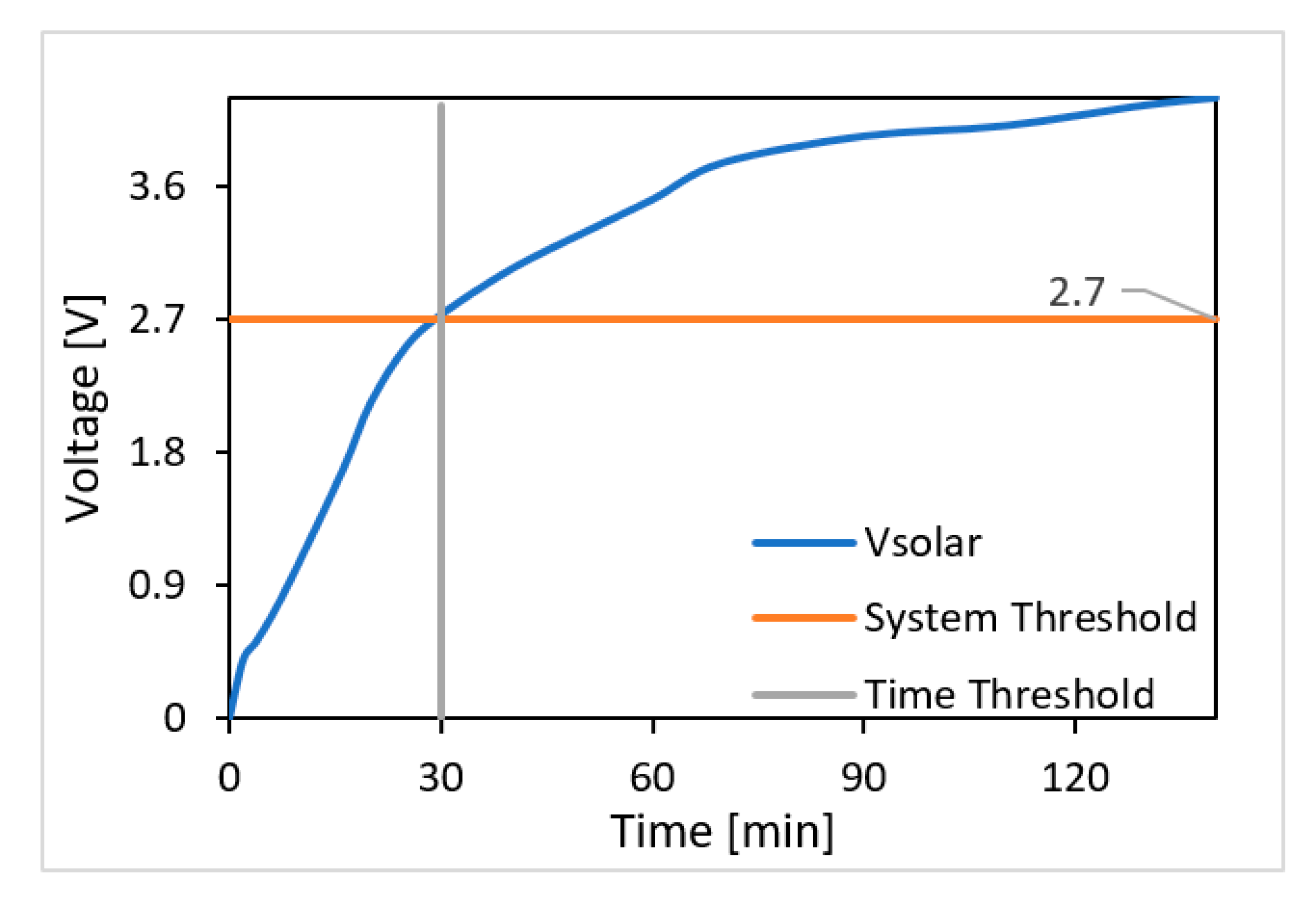
Figure 4 shows the time it takes for the solar module to charge the supercapacitor on a sunny day. The vertical grey line in 30 min and the horizontal orange line in 2.7 V indicate the time and voltage, respectfully, needed to turn on the device. This means that the device must be exposed to the sun for 30 min before it turns on because this is the time needed to reach 2.7 V. The highest value for the supercapacitor is 4.2 volts, which is maintained after being reached.
There are four graphics in
Figure 5, which show the drop of voltage throughout the day in a shady place for several days. The first shows the drop during the night, the next two show the drop during some hours with daylight, and the last is a zoom of the curve of the last picture. The horizontal orange line is the threshold at which the system is on, which is checked when the LED turns on and, as is already known, happens at 2.7 V. The blue line is a square curve that represents when the system turns on with “1”, and when system turns off with “0”.
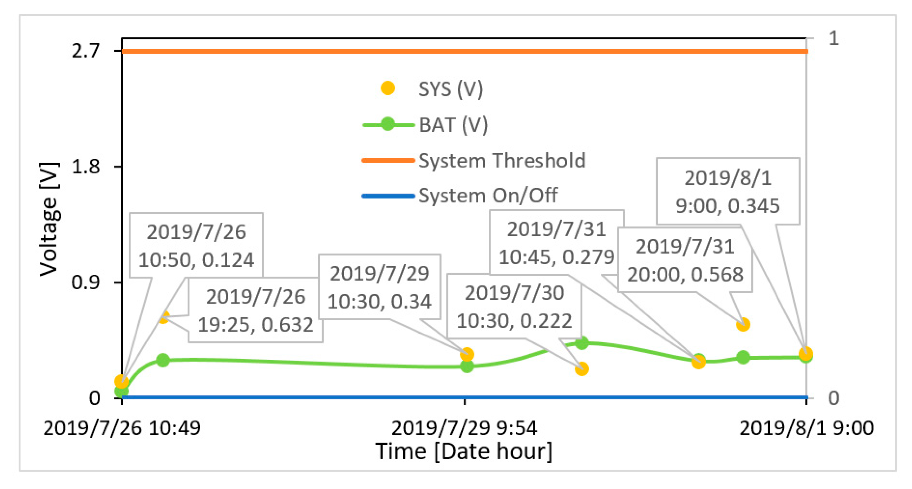
The mechanical module was tested with the tag in the same place for several days, and the charge measurements of the supercapacitor are reflected in
Figure 6. SYS is represented by points because it collected a lot of energy with every car that passed; but then, if no cars passed, the voltage dropped quickly, so a continuous signal would, in this case, not be real. In BAT, the voltage is maintained for longer because it is saved in the supercapacitor, so the line in the graphic is continuous. The threshold voltage to turn on the tag is represented by the horizontal orange line.
3.2. Complete Tag
Now, the results of testing the processing module with the supercapacitor as the source of energy are shown. The device turns off when the voltage in the supercapacitor is 2.7 V, as is commented below.
3.2.1. Low Power Consumption Scenario
The results of this test scenario are shown in
Figure 7. In
Figure 7a, the voltage drop over time can be seen, and is represented until the working limit of 2.7 V.
Figure 7b shows the current associated to the low power mode and
Figure 7c shows the transitions associated to the current when this scenario is running.
With a voltage of 4.2 V in the supercapacitor, the consumption in reception mode is around 7 mA and the low power mode is around 31.85 µA, which, considering the theoretical values, are the expected values. In terms of energy, taking into account that, in our test, the time in low power mode is 0.5 s, the energy needed for the low power mode is 66.89 µJ. The peaks of reception use 14.7 mJ for the other 0.5 s.
3.2.2. Transmission Scenario
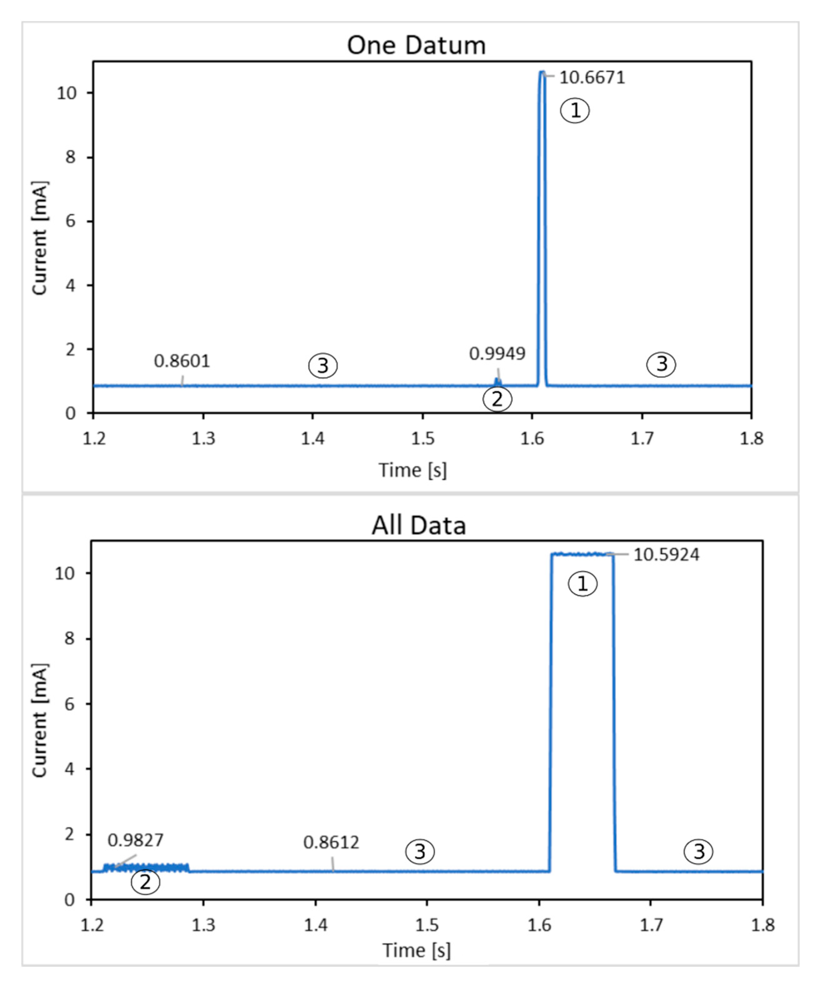
The data are transmitted periodically at a rate of one package per second.
Figure 8 displays the currents for transmitting one datum and a data package with 4.2 V in the supercapacitor. The lower consumption line pertains to the microcontroller due to its continuous active mode. The time needed to perform the transmission of a data package is higher than that needed to perform a transmission of one datum. In addition, the consumption for both graphics are similar for each element, as can be seen in the values of the figure.
The time needed to complete one of these transmissions is approximately 50 milliseconds for a package with a simple datum and 450 milliseconds for a data package of maximum length, as can be seen in
Figure 8.
The associated energy to transmit one datum starts with the peak in the EEPROM. The value is calculated with the sum of the EEPROM energy, 16.7 µJ, the transceiver energy, 127.9 µJ, and the microcontroller energy between the last two, 313.6 µJ. The total is 458.2 µJ for one datum.
In the case of all data it is calculated in the same way than for one datum. The values are: 272.4 µJ for the EEPROM, 1.17 mJ for the transceiver and 2.54 mJ for the microcontroller. The total is 3.98 mJ for all data.
3.2.3. Reception Scenario
In this scenario, the transceiver stays in reception mode and the microcontroller in the active mode for all commands. The current consumption for the transceiver in reception mode is 7.6 mA and for the EEPROM in active mode is 0.99 mA in all cases. The value in the supercapacitor for the measurements is 4.2 V.
First, the “read one” datum from EEPROM, represented in the upper graphic of
Figure 9. The time required for the whole operation is approximately 100 milliseconds. The associated energy of this command, since the moment that transceiver changes their mode, is: 12.5 µJ for the EEPROM, 268.8 µJ for the transceiver and 317.9 µJ for the microcontroller; a total of 599.2 µJ.
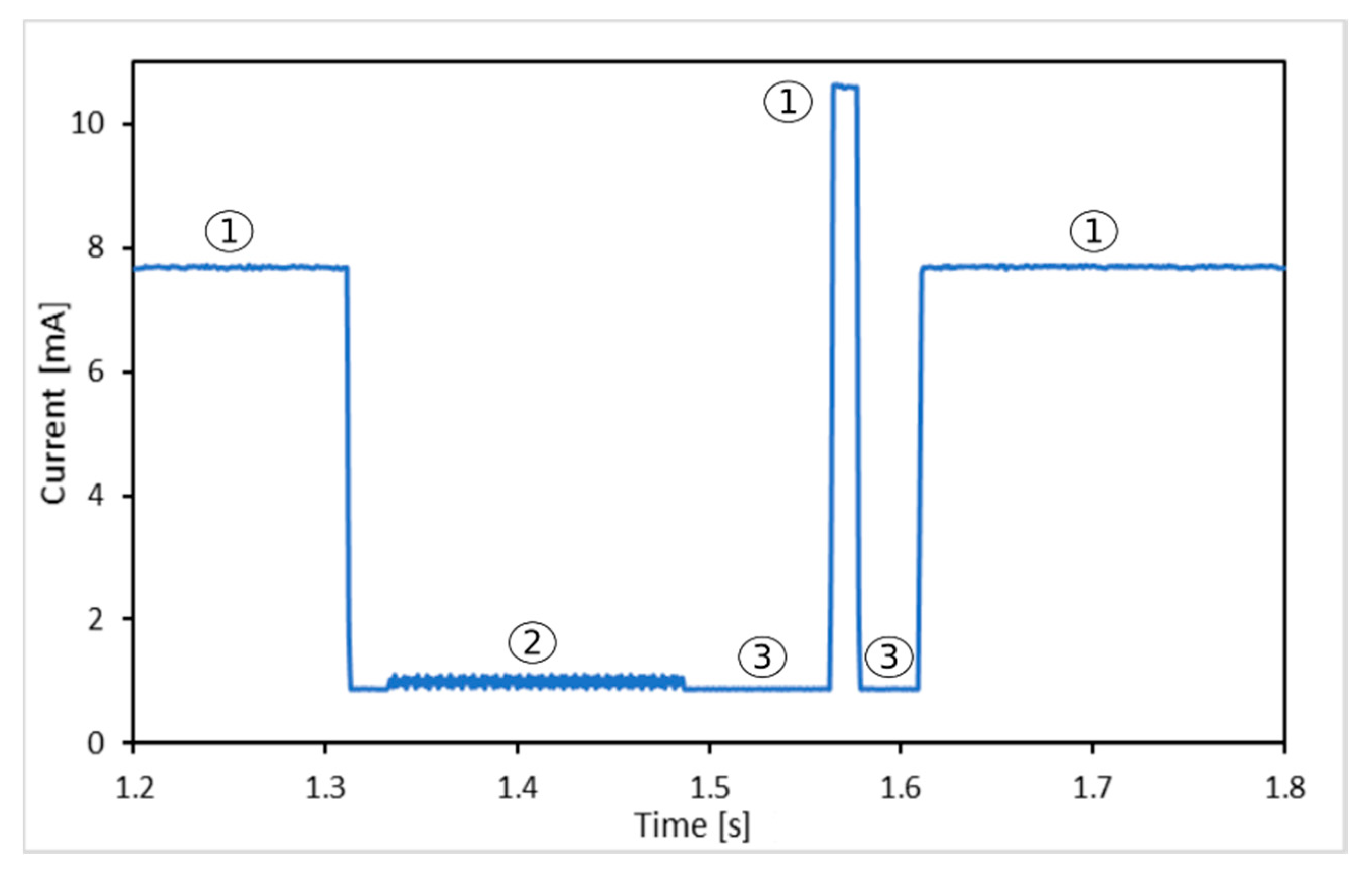
Second, the reception of the “read all data” command from EEPROM, as can be seen in the lower graphic of
Figure 9. The current consumption is the same as that previously commented for EEPROM, around 0.99 mA, and for the transceiver in every transmission, around 10.6 mA, for the three that this read all data command requires. The time spent in the complete command is around 2.2 s. The associated energy to the command, considering the three packets needed to complete it, are: first transmission: 311.75 µJ for the EEPROM, 2.54 mJ for the transceiver, and 1.37 mJ for the microcontroller; second transmission: 228.7 µJ for the EEPROM, 1.96 mJ for the transceiver, and 1.1 mJ for the microcontroller; third transmission: 0 J for the EEPROM, 0.22 mJ for the transceiver, and 0.3 mJ for the microcontroller. The energy needed between transmissions are 19.79 mJ and 18.22 mJ. The wasted energy for this command is 46.04 mJ.
Third, “read date”,
Figure 10. The consumption is around 0.99 mA for EEPROM and 10.6 mA for transmission, as in previous commands. The time for this command is around 300 milliseconds. In this case, the associated energy, since the point that the transceiver changes the mode, as in the other commands is: 636.2 µJ for the EEPROM, 623.3 µJ for the transceiver, and 467.7 µJ for the microcontroller; energy of 1.73 mJ in total.
Finally, the last implemented command is “write”. The entire process is shown in
Figure 11. The total command time is around 157 milliseconds. The associated energy is 567.6 µJ in total, 70.7 µJ for the EEPROM, and 496.9 µJ for the microcontroller.
4. Discussion
As shown in the results obtained in a real scenario, solar energy is dominant over mechanical, since it obtains more energy in an environment that is always changing and is unpredictable. This technique is the bottleneck of our device because the weather cannot be estimated accurately, so the amount of energy obtained cannot be predicted, it is, that is the point with the most uncertainty. In the shady zones, the device might not work continuously due to all the hours of sunlight the device is in the shade. Consequently, for the final device, it is important to minimize or eliminate the hours in which the device is in a shady zone. However, the limiting case of solar energy comes from the voltage drop during the night, as can be checked in
Figure 4. This means that if we want the device to stay on continuously, it will be important to characterize those conditions in future implementations because this application is related to an enclosed framework, where the sun is needed for a positive energy balance. If the weather of the place where the tag is implemented is usually cloudy, or the days are short during a great part of the year, this solution will not be optimal, although a previous study must be done to corroborate this. These conditions can be considered as the constraints of the work since the conditions limit the energy obtained to work. Focusing on the board, there is no concrete limit for consumption, energy or size, the work pursuit the lowest power consumption, the most energy obtained, and the smallest size (as a portability and environmental matter).
Nevertheless, for mechanical energy, it can be seen that the system is not capable of working in those environmental conditions. The maximum values of collected mechanical energy (in SYS), which are probably due to an increase in road traffic, are not enough to turn on the system if this technique were the only one working in the device. When a vehicle passes near the tag, the voltage in the supercapacitor increases and then drops quickly. The average collected energy is not enough to charge the supercapacitor. The same applies to the BAT output, although the voltage is maintained longer for BAT, because this output is connected to the supercapacitor. So, the contribution of this technique to the charge and running of the system is very low. A higher inflow of cars and with higher speeds is necessary to allow the system to use only this technique as the main technology and to consider an option to include it in future versions. In a final device, for this application, mechanical energy will not be included. However, for other applications, it can be very interesting to consider this energy. Consequently, whether to include it or not should be valued depending on the scenario.
As for the processing module, it is shown that the consumption is adequate for applications such as the one at hand. The energy consumption peaks correspond to transmissions and receptions, which can be sustained by the energy collected in the supercapacitor, as the system is still working after these said peaks. Consequently, the device will remain on over time for whatever scenario. Staying in one scenario or another is variable and depends on the application. Such new applications may require a different supercapacitor, or only one of the two available energy harvesting modules, etc. Including a battery can cause a malfunction due to the fact that it is not capable of handling transmission and reception peaks as well as the supercapacitor. Furthermore, it requires a long time to charge and decreases the lifetime of the system because it has fewer cycles. Therefore, a battery should not be included in the next designs.
For this first prototype, in the low power consumption scenario of this application explained above, with the supercapacitor fully charged and no external source of power, the tag is able to function autonomously for 7 min, as can be checked in
Figure 7a. When the tag is placed on the traffic sign, with the energy harvesting modules connected. An autonomy of 10 h is achieved, and this is a parameter needed to characterize this device and really prove that it is autonomous. This is due mainly to solar energy, which can recharge the supercapacitor after the peaks of reception that are acceptable to the tag. However, it has to be considered that it depends on the environment and the application. The device, for this application, will work during daylight hours where the dominant mode is the low power consumption scenario with a duty cycling of 50%. However, the duty cycling can be reduced to 0.2%, which means that the consumption is 25 times less and thus increases the lifetime. This value for duty cycling is considered the optimal value for the device because it is the lowest value for which the transceiver is able to work correctly. Therefore, in the final application, this will be the value for the reception mode. This tag prototype turns off during the night, but the previous change in reception values and the option to replace the supercapacitor with a larger one will give the tag full autonomy for the whole day, although a study should be done. If there is enough energy, the scenarios work regardless of the time of day.
The usability of this tag as a self-powered device can be guaranteed thanks to
Figure 5, where the device supports every peak of the transceiver and is able to continue working. Assuming the change in the duty cycling and the solar source power, the autonomy and viability of using this device as the final self-powered device will have to be checked again.
The abovementioned points highlight the need for a specific solar panel, piezoelectric, and supercapacitor, as well as the configuration of the built-in low power consumption modes according to the end application for an optimal optimization of the device. This also requires a prior study of the conditions of the set-up location, under what conditions the application will be used and which requirements the tag will need. This prior work will allow the maximum exploitation of the energy harvesting submodules and the regulation and storage submodule to obtain the best performance regarding energy and lifetime. Although no comparison has been done to check the optimization of the processing module, we have made an effort to find the best configuration of the different components in order to achieve the minimum consumption according to the manufacturer’s information.
This study is performed to cover the autonomous active tags applications, which have a mode called low power consumption, where the consumption is as low as 31.85 µA (66.89 µJ), with peaks of 7 milliamperes for reception (14.7 mJ), which is a good low consumption.
Taking into account the energy that the supercapacitor is available to store when is full charged and looking at the energy requirements of the device in every scenario, it is clear that the energy balance is positive. The command that needs more energy is “all data” in reception scenario due mainly to the energy wasted between transactions, something that has to be checked for the final application. Moreover, the reception peaks have a high energy consumption, this point supports the previous idea of reducing the duty cycle.
The tag could be used in almost every environment initially considered, which turns this device into a useful system. However, depending on the requirements of the working modes, the time it is alive will be different. Furthermore, the consumption of the components could be reduced and the supercapacitor can be replaced if the energy requirement of this application does not fit the one needed for the new application, so the useful time would be longer.
The tag case prevents it being damaged by dust or water. The sensitivity of the device is the same as all electronic circuits; in the presence of such extreme weather conditions as high temperatures or humidity, over time, the tag can be damaged. Nevertheless, it is the task of the mechanical encapsulation to prevent this from happening.
The complete tag only has installation costs, since maintenance is not contemplated. The design of the tag has been conceived to give it a longer lifetime. However, in the case of incorrect operation, the tag will be replaced because the installation is easy and our tag is scalable. This means that our tags do not need any maintenance. Taking into account the materials and the cost of the board, one tag costs approximately 50 euros, not including the labor costs. Mass production would reduce the cost of the tag.
5. Conclusions
Autonomous active tags powered by a supercapacitor and solar and mechanical energy harvesting modules, capable of working independently for storing, transmitting and receiving information are viable for one application made from a project with a company. Consequently, this can be extrapolated to other applications, such as those related to V2I or smart houses. The tag has been tested in an outdoor scenario that fits our purposes and, given the results, we conclude that some parameters depend on the application, which are related to the different modes in which the transceiver, the microcontroller and the EEPROM can operate, and to the energy requirements that are basically based on a solar panel and supercapacitor. In addition, the use of a supercapacitor instead of a battery gives the tag a longer independent life.
There is a great uncertainty in the amount of energy that is available in every moment as this energy depends on external factors as the sun or the cars. So, the different modules and the integration of them have been developed to work in the best possible way to obtain the larger quantity of energy and to use it to the tag has a greater autonomy.
As has been said before, possible applications are not only roads and traffic signs but every environmental situation, such as the roof or a window of a house, or even a car. In an environmental situation, there are such variables as the temperature that can be saved to keep a record of the variations. Perhaps this information could be sent to another device in the communication range or to a reader that comes for the data. It could be the same inside a house, to monitor the temperature of different rooms, or to automatically control and monitor some elements like the air conditioning, the doors or even electrical appliances. All these are examples of what is now known as an IoT (Internet of Things) node. However, in our case, it is not necessary to plug it into the node to get power or change the battery when it is depleted.
On the other hand, scenarios where there is a heavy load would be difficult to support, even with a great supercapacitor.
As there is no other tag with the features and functions presented in this work, we consider that this solution is competitive and affordable for this application. The autonomy is defined, a parameter that other studies do not usually contemplate, and which we consider to be an important value to characterize the system, improve it and really know that it is autonomous. The integration of the different techniques is a good way to improve the functionality and scope of this work for a real environment.


