Article

Cascaded Nanorod Arrays for Ultrabroadband, Omnidirectional and Polarization-Insensitive Absorption

1
Department of Photoelectric Information Science and Engineering, School of Science, Jiangnan University, Wuxi 214122, China
2
Jiangsu Provincial Research Center of Light Industrial Optoelectronic Engineering and Technology, Jiangnan University, Wuxi 214122, China
*
Author to whom correspondence should be addressed.
Appl. Sci. 2020, 10(11), 3878; https://doi.org/10.3390/app10113878
Submission received: 8 May 2020 / Revised: 31 May 2020 / Accepted: 1 June 2020 / Published: 3 June 2020
(This article belongs to the Special Issue Active Nano Optics)

Abstract

:
An ultrabroadband, omnidirectional, and polarization-insensitive absorber based on cascaded nanorod arrays (CNAs) is numerically demonstrated, and an average absorptivity of 98.2% with a relative absorption bandwidth (RAB) of 149.8% can be achieved in the 0.38–2.65 μm wavelength range. The proposed CNA-based absorber requires only several pairs of multilayers to achieve excellent absorption performance. More significantly, the physical mechanism for this intriguing ultrabroadband absorption results from the synergistic effect of localized surface plasmon (LSP) and plasmonic resonant cavity (PRC) modes, which is fundamentally different from the tapered metal/dielectric multilayer-based absorbers associated with the slow-light mode. We investigated the absorption properties of the CNA-based metasurface by using the impedance theory, which indicates that the impedance of the structure matches well with the impedance of the free space from the visible to near-infrared wavelength range. In addition, the absorption properties of the CNA-based metasurface are robust to the variation of the structural parameters and the metal/dielectric materials, and ultrabroadband absorption performance can be maintained within 0–60° for both TM and TE modes.

Graphical Abstract

1. Introduction

Plasmonic absorbers can function as crucial components for various applications such as sensing [1,2], photodectors [3], thermal emitters [4,5], photovoltaics [6,7], etc. In the past decade, the metal-insulator-metal (MIM) nanopatterned structures are the main schemes to achieve perfect light absorption enhancement [8]. In this configuration, strong electromagnetic coupling could be excited between the metallic pattern and the metallic substrate in a small wavelength range due to magnetic or electric resonance. By choosing different shapes of metal patterns such as strip [9,10], square [11,12], hole [13], disk [14] and # [15], perfect absorption can be obtained as impedance matching is satisfied at a specific wavelength. However, the resonant characteristics of the conventional MIM absorbers result in narrow bandwidths, which may limit their applications in the fields of IR cloaking, solar cells, and imaging. To meet the demand of broadband absorption, some broadband absorbers have been proposed by using the concept of a superlattice. By integrating multi-sized resonators such as strips [16,17], squares [18,19,20,21], disks [22,23], and crosses [24,25] into the unit cell, or using multi-thickness metasurfaces [26,27], multi-band or broadband absorption can be obtained due to the overlapping of multiple resonance frequencies. Unfortunately, the bandwidths of these absorbers are limited by the possible number of resonators that can be integrated into the subwavelength superlattice.
In recent years, hyperbolic metamaterials (HMMs) have become an active research area due to exotic hyperbolic dispersion, which originates from one of the principal components of their electric or magnetic effective tensor having the opposite sign to the other two principal components [28]. It has been shown that HMMs can be used to improve light absorption due to their high-wavevector propagating modes and enhanced photonic density of states [29,30]. In general, a thin-film multilayer consisting of alternating metal/dielectric layers will give rise to hyperbolic dispersion because the layer thicknesses can be ignorable compared with the operating wavelength. By using hyperbolic metal/dielectric multilayers [31,32], nanostrips [33], or nanopillars [34], light absorption can be efficiently enhanced in a small wavelength region. To broaden the absorption bandwidth, more complicated HMM nanostructures with graded metal/dielectric patterns, such as sawtooths [35,36,37,38,39,40], pyramids [41,42,43], and nano-cones [44,45,46,47] are required. Similarly, by integrating multi-sized, graded HMM patterns into the unit cell, the absorption bandwidth of the graded HMM absorbers can be further expanded [48,49]. Generally, the physical basis for the intriguing ultrabroadband absorption of these HMM-based absorbers is associated with the slow-light effect. As the incident light is coupled into the taped HMM-based waveguide, the group velocity of the waveguide mode at different wavelengths will be reduced dramatically at their corresponding critical widths, which enables the collective excitation of slow-light waveguide modes over a broad wavelength region, also known as the trapped rainbow phenomenon [50,51]. Although the achieved absorption results of the HMM-based absorbers are remarkable, their fabrication process is quite challenging due to the graded metal/dielectric patterns with a large number of film stacks. Furthermore, despite the elaborate study of nanostructured plasmonic absorbers, absorption performance that combines the advantages of high absorption efficiency, ultrabroad bandwidth, and omnidirectional characteristics is still highly desired.
Inspired by these earlier works, here we demonstrate a novel ultrabroadband, omnidirectional, and polarization-insensitive absorber based on cascaded nanorod arrays (CNAs). The CNA-based absorber requires only several metal/dielectric stacks, and an average absorptivity of 98.2% with a relative absorption bandwidth (RAB) of 149.8% can be achieved in the 0.38–2.65 μm wavelength range. The physical mechanism for ultrabroadband light absorption of the CNA-based absorber results from localized surface plasmon (LSP) mode, plasmonic resonant cavity (PRC) mode, and their hybrid modes, which is fundamentally different from the tapered metal/dielectric multilayer-based absorbers associated with the slow-light mode. In addition, the absorption characteristics of the CNA-based absorber are robust to the variation of the structural parameters and the metal/dielectric materials, and omnidirectional absorption performance can be realized due to high angular tolerance for both TM and TE polarizations in the range of 0–60°.

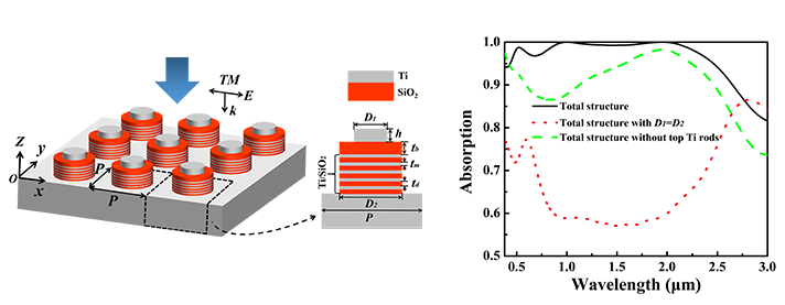
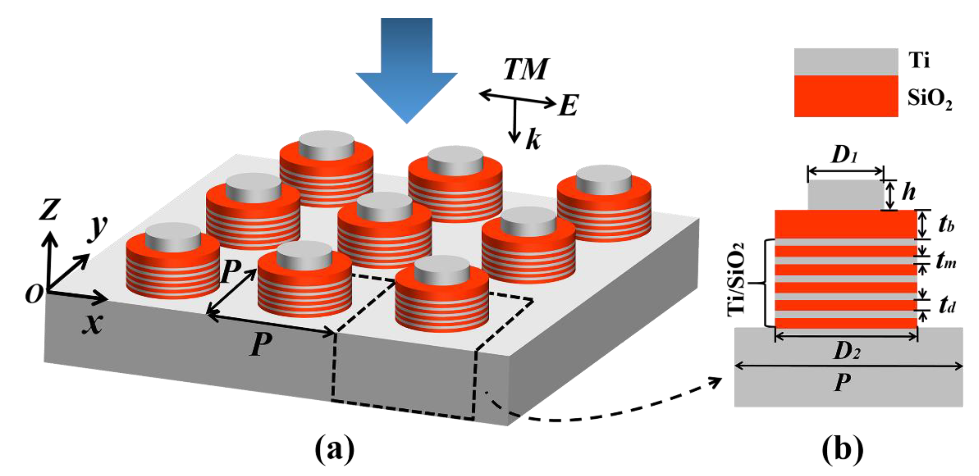
2. Structure and Design

Figure 1 shows the schematic map of the CNA-based metasurface under the TM (electric field along x-axis) wave illumination. The unit cell of the CNAs consists of two types of nanorods. One is the top metal (Ti) nanorod with height h and smaller diameter D1, the other is the bottom metal/dielectric (Ti/SiO2) multilayer nanorods with larger diameter D2, and these two types of nanorods are separated by a dielectric (SiO2) buffer layer with thickness tb. The number of the alternating Ti/SiO2 pairs (N) of the multilayer nanorods is 5; the thickness of each Ti and SiO2 film of the multilayer nanorods are tm and td, respectively. P is the period in the x and y directions. The background is air. The thickness of Ti substrate is chosen as 200 nm to block the light transmission. The refractive index of SiO2 is 1.47, and the dielectric constant of Ti is obtained from Palik [52].
For the CNA-based metasurface at normal incidence, whether a diffraction order propagates or not in the background can be written as [53]
m 2 + n 2 < P 2 / λ 2
where m and n are the diffracted orders along the x and y directions, respectively. λ is the wavelength in free space. To ensure ultrabroadband absorption, a subwavelength unit cell with P < λ should be chosen to avoid the energy transfer via high-order diffraction.
In simulations, we adopted the three-dimensional finite-difference time-domain (FDTD) method to analyze the absorption performance of the CNA-based metasurface. The absorption of total structure can be simplified as A = 1 − R due to the optically thick Ti substrate, where R is the reflection of the structure. Moreover, the absorption of different parts of the structure can be extracted by integrating power dissipation of every single layer [12,54,55]:
α ( λ ) = 1 2 ε 0 ω Im ε ( ω ) V | E | 2 d V
where ε0 is the permittivity of vacuum, ω is the angular frequency, ε denotes the relative dielectric permittivity of each layer, Imε(ω) is the imaginary part of ε, E denotes the amplitude of electric field, and the integral is over the desired part of a unit.
In addition, the average absorption within the operating wavelength region is used to evaluate the overall absorption performance of the CNA-based absorber, which can be calculated as
A a v = 1 λ L λ S λ S λ L A ( λ ) d λ
where λL and λS are the larger and smaller limits of a wavelength region with absorptivity higher than 90%. Furthermore, to compare the absorption bandwidth of the CNA-based absorber with that of other types of broadband absorbers, the RAB is introduced, which is generally defined as RAB = 2(λLλS)/(λLλS) [56].

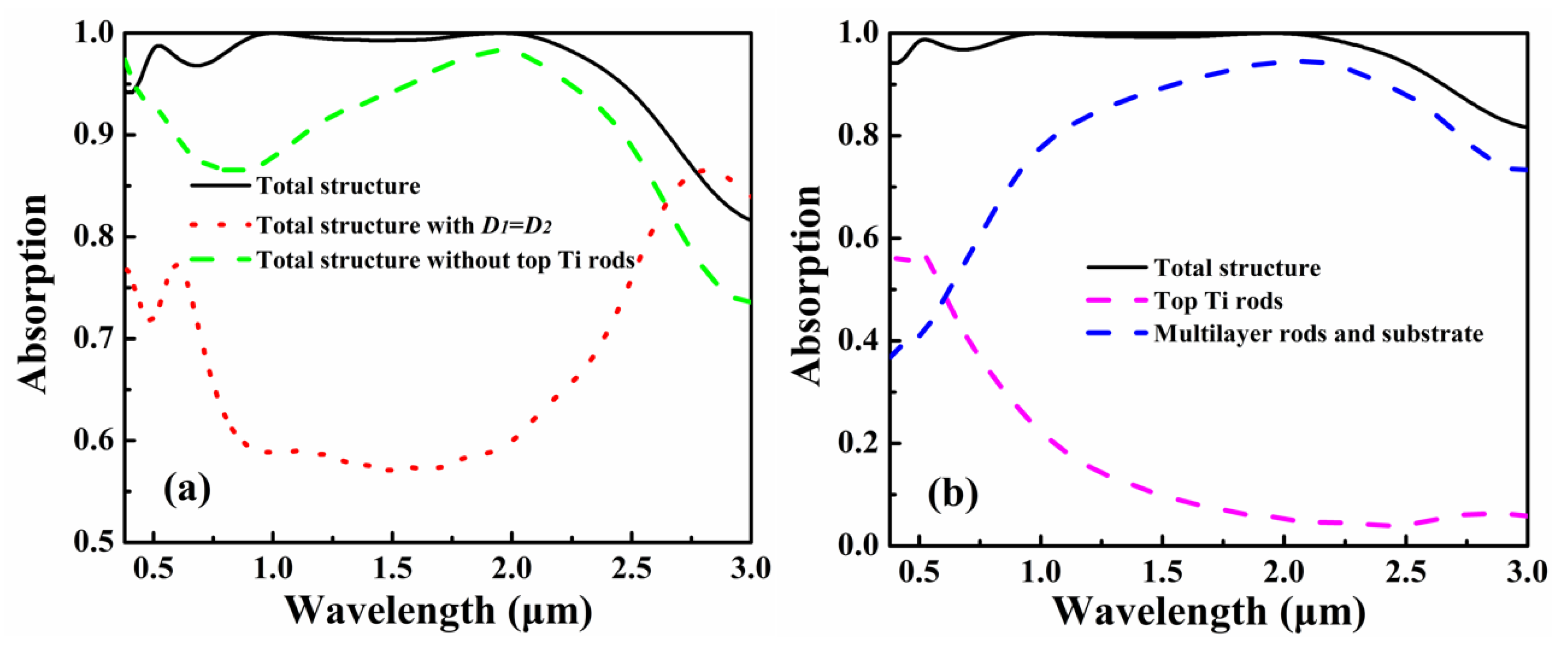
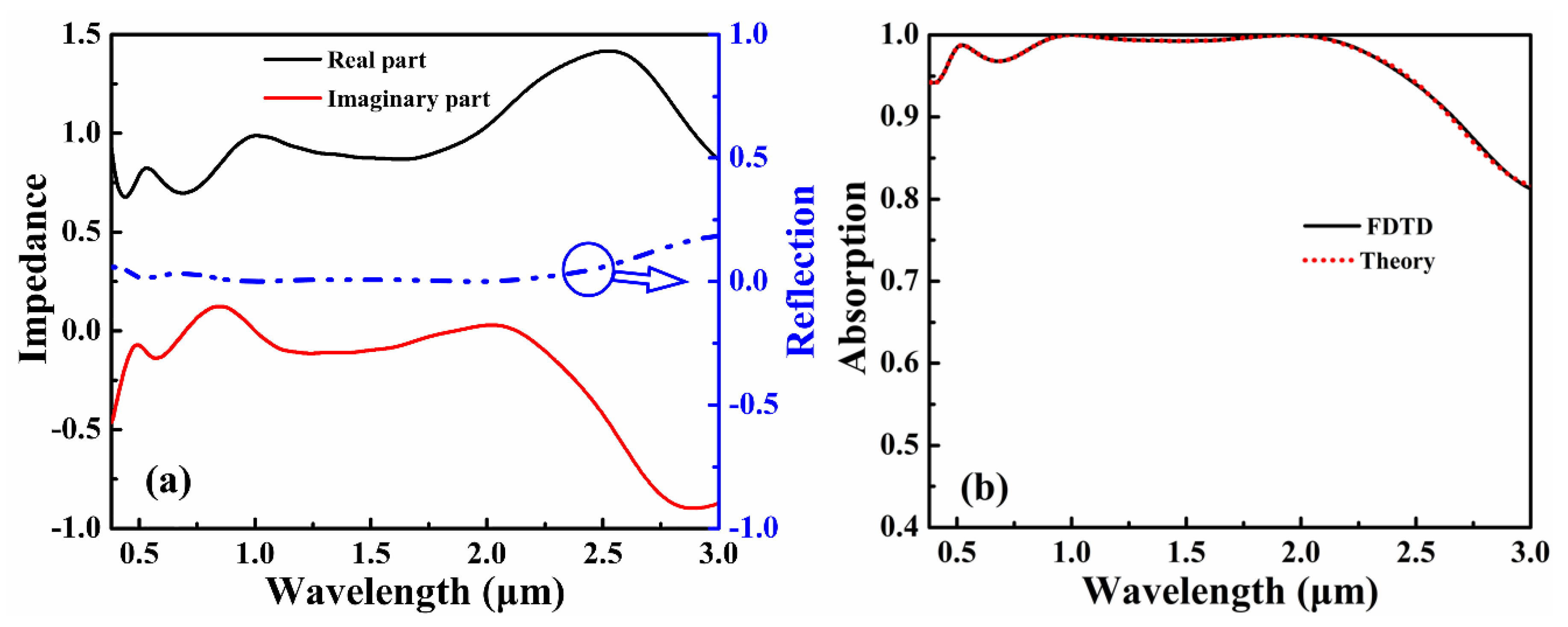
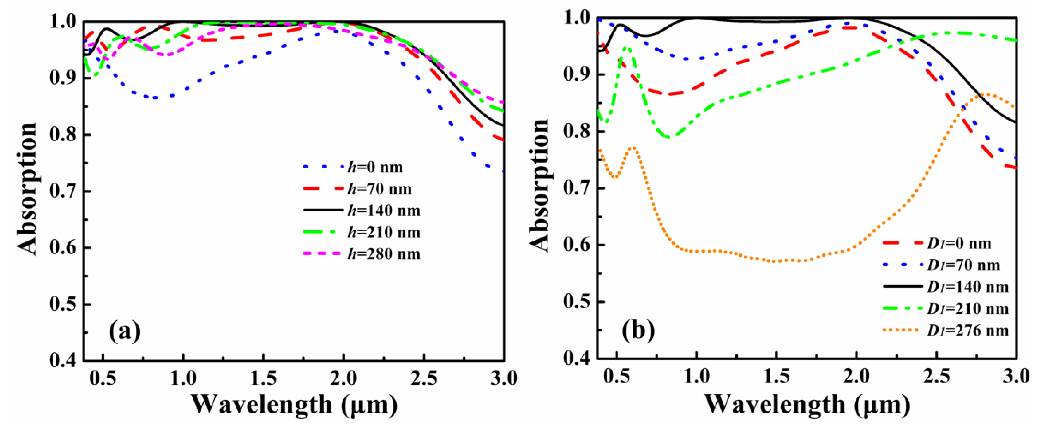
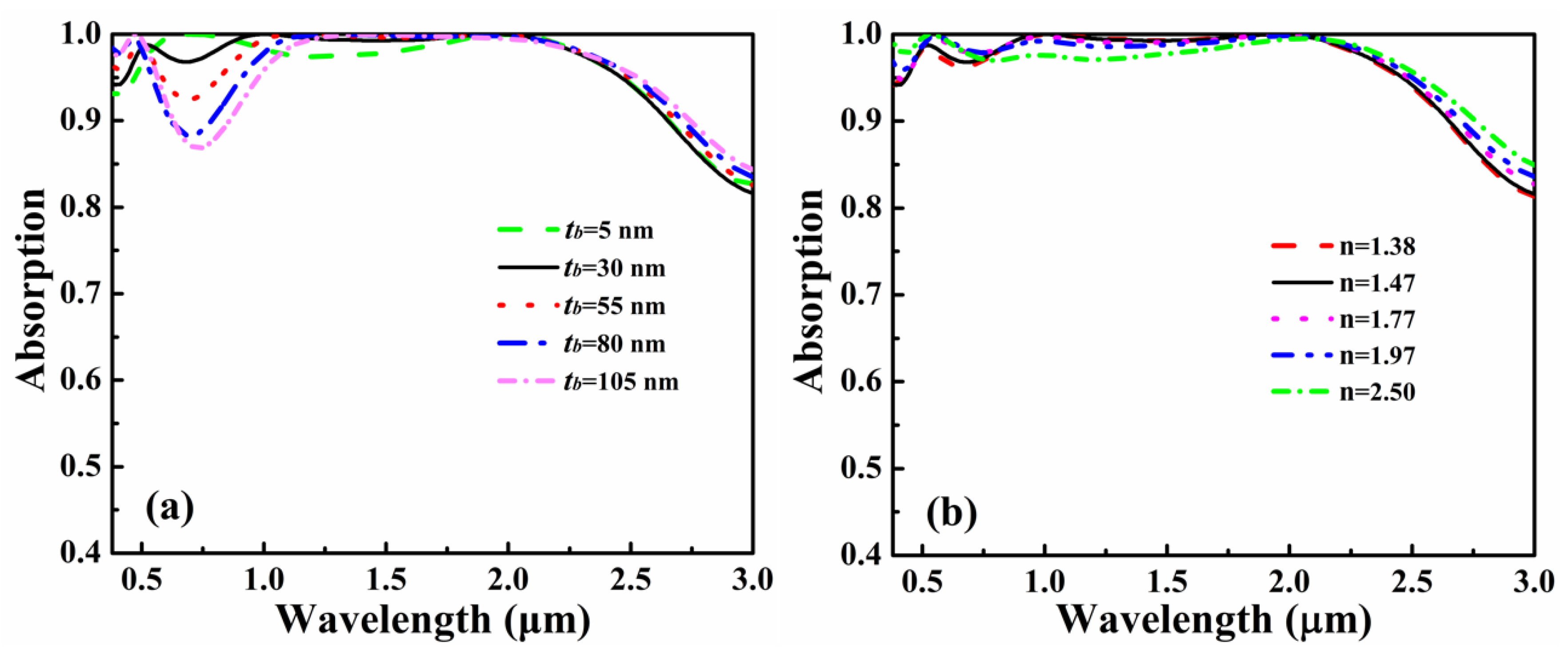
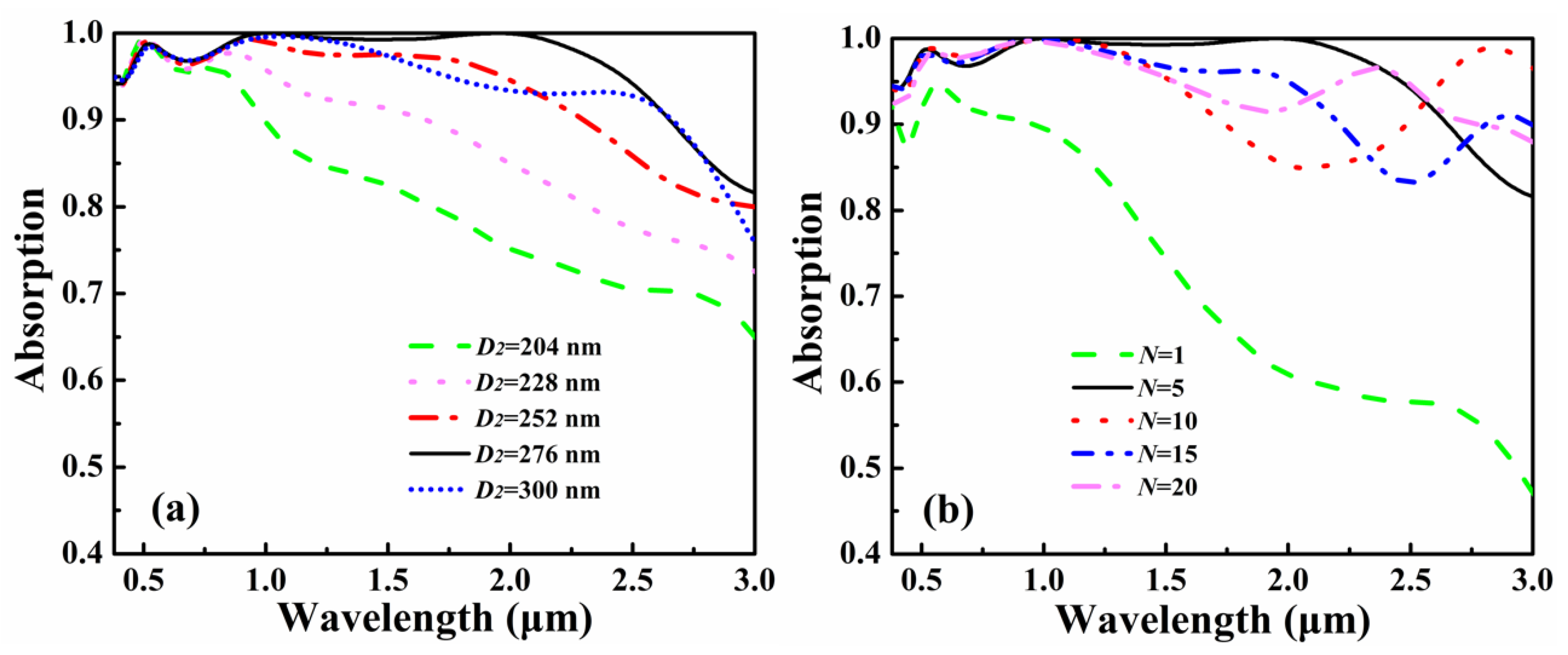
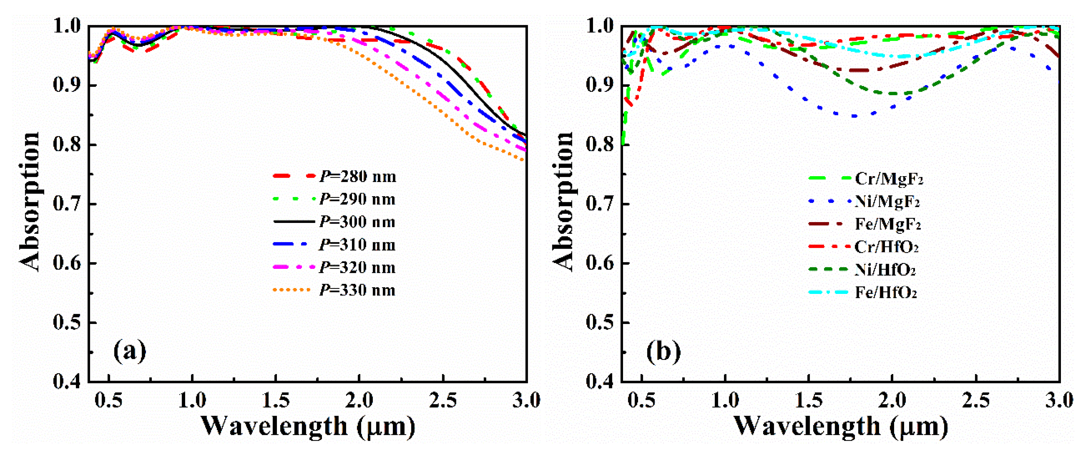
3. Absorption Performance Analysis

Figure 2 shows the absorption performance of different CNA-based structures. As indicated in Figure 2a, ultrabroadband absorption enhancement can be obtained for the CNA-based absorber from the visible to the near-infrared region, and three absorption peaks occurred at the locations of 0.524 μm, 1.001 μm, and 1.952 μm. An average absorptivity with Aav = 98.2% and RAB = 149.8% can be achieved in the 0.38–2.65 μm wavelength range. Note the RAB of the CNA-based absorber is larger than many types of broadband absorbers such as multi-sized MIM absorbers [16,17,18,19,20,21,22,23,24,25], multi-thickness absorbers [26,27], and graded HMM absorbers [35,36,37,38,39,40,41,45,46,47]. The RAB of the CNA-based absorber is also comparable with that of multi-sized graded HMM absorbers [48,49]. Specifically, compared with the similar structure of 3 × 3 cascading metal-dielectric pairs, in which the ultrabroadband absorption results from the overlapping of the magnetic resonances of three subunit cells [57], the absorption performance (i.e., RAB, average absorptivity, polarization and angle independent features) of the CNA-based absorber is better because it combines the advantages of LSP and PRC within a comparatively simple and low-cost configuration. However, for the CNA-based structure with D1 = D2, the broadband absorption performance of the structure is out of function, and the absorption band with absorptivity above 90% disappears completely in the whole spectral wavelength region. In particular, for the CNA-based structure without top Ti nanorods, the absorption of the structure is significantly reduced in the shorter wavelength region. In Figure 2b, we calculate the contributions of the top Ti nanorods and the rest of the CNA-based metasurface to total light trapping. As shown in Figure 2b, the absorption of the CNA-based absorber mainly results from the multilayer nanorods and substrate, yet a non-ignorable amount of absorption originates from the top Ti nanorods in the region of 0.38–1.5 μm. Therefore, the top Ti nanorods are essential for the absorption enhancement of CNA-based absorbers in the short wavelength region.
To better understand the physical mechanism of the ultrabroadband absorption enhancement of the CNA-based metasurface, the distributions of electric field and energy flows are investigated at the locations of three absorption peaks. As indicated in Figure 3a, for the short wavelength of 0.524 μm, the electric field is enhanced mainly around the corner of the top Ti nanorods, exhibiting the features of localized surface plasmon (LSP) mode [58,59]. In addition, the distribution of the Poynting vector shows that energy of the incident light primarily flows and dissipates around the surface of the top Ti nanorods, resulting in the absorption enhancement of the short wavelength. As can be seen in Figure 3c, for the long wavelength of 1.952 μm, the electric field is mainly enhanced and localized in the narrow cavities formed by the adjacent multilayer nanorods, showing the features of plasmonic resonant cavity (PRC) mode [60,61,62]. The energy flow of the incident light propagates along the −z direction, and the energy of light is mainly confined and consumed by the narrow cavities and the metallic substrate. As shown in Figure 3b, for the middle wavelength of 1.001 μm, the electric field is enhanced by the top Ti nanorods and the narrow cavities simultaneously, and the energy flows are trapped by both of them, indicating the hybrid LSP and PRC modes. Therefore, the ultrabroadband absorption of the CNA-based metasurface originates from the synergistic effect of the LSP and PRC modes. It is interesting to note that although several metal/dielectric multilayers are required for the CNA-based absorber, its physical mechanism for ultrabroadband absorption is fundamentally different from the tapered metal/dielectric multilayer-based absorbers associated with the intrinsically slow-light mode [35,36,37,38,39,40,41,42,43,44,45,46,47,48,49]. That is, these metal/dielectric multilayer-based absorbers can be equivalent to the anisotropic metamaterials with tapered width, and each metal/dielectric/metal layer acts as an independent slow light waveguide to stop and consume the light energy of a particular wavelength.
In order to figure out the link between the ultrabroadband absorption performance and the related electromagnetic parameters of the CNA-based metasurface, we also investigate the input impedances of the structure by using the impedance theory. By using the impedance theory [63,64], the impedance Z of the CNA-based metasurface can be expressed as
Z = ± ( 1 + S 11 ) 2 S 21 2 ( 1 S 11 ) 2 S 21 2
S 11 = S 22 = i 2 ( 1 Z Z ) sin ( n k d )
S 21 = S 12 = 1 cos ( n k d ) i 2 ( Z + 1 2 ) sin ( n k d )
where S11, S21, S12, and S22 are S parameters; and n, k, and d are the effective refractive index, the wave vector, and thickness of the structure, respectively. Therefore, the relation between the theoretically calculated reflection of CNA-based structure and the impedance Z can be simplified as R = [(ZZ0)/(Z + Z0)]2, where Z0 is the impedance of free space.
Figure 4a shows the reflection response and impedance of the CNA-based metasurface. The parameters are the same as those in Figure 2b. As shown in Figure 4a, the real part of Z approaches one and the imaginary part of Z tends to zero in the wavelength range of 0.38–2.5 μm, resulting in the ultrabroadband antireflection with R ≈ 0 in this wavelength region. Figure 4b shows the FDTD and the theoretical results of the absorption response of the CNA-based metasurface. Herein, the theoretical results are calculated by using the retrieved input impedances, which show excellent agreement with the FDTD results.

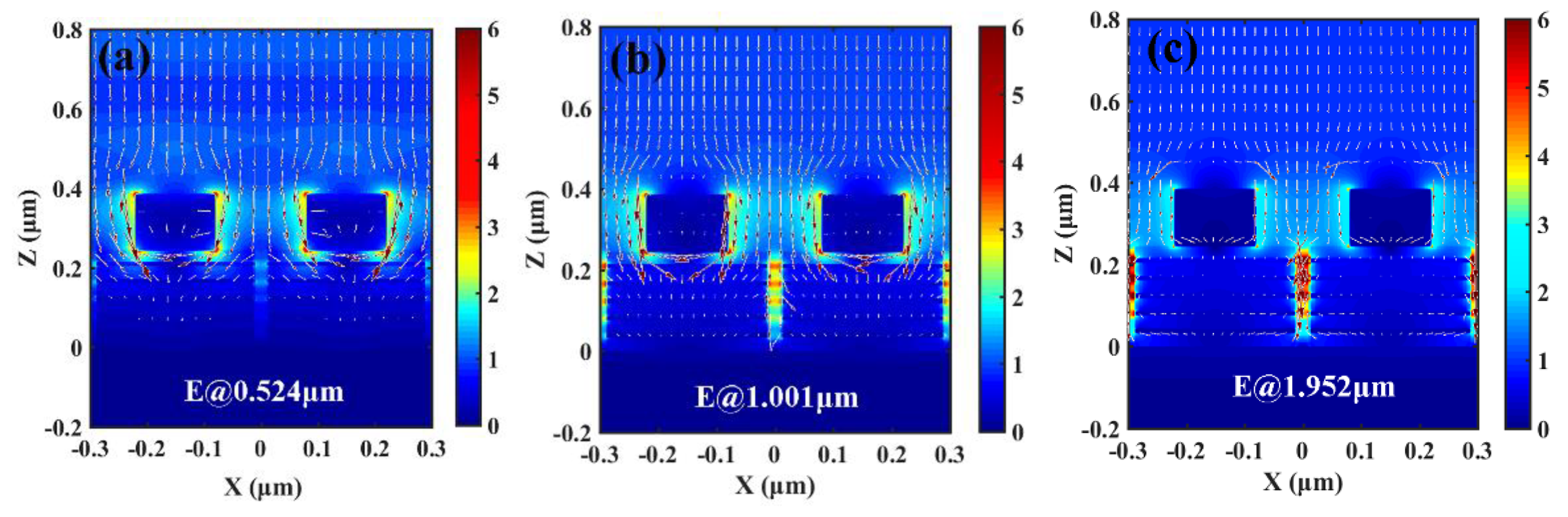
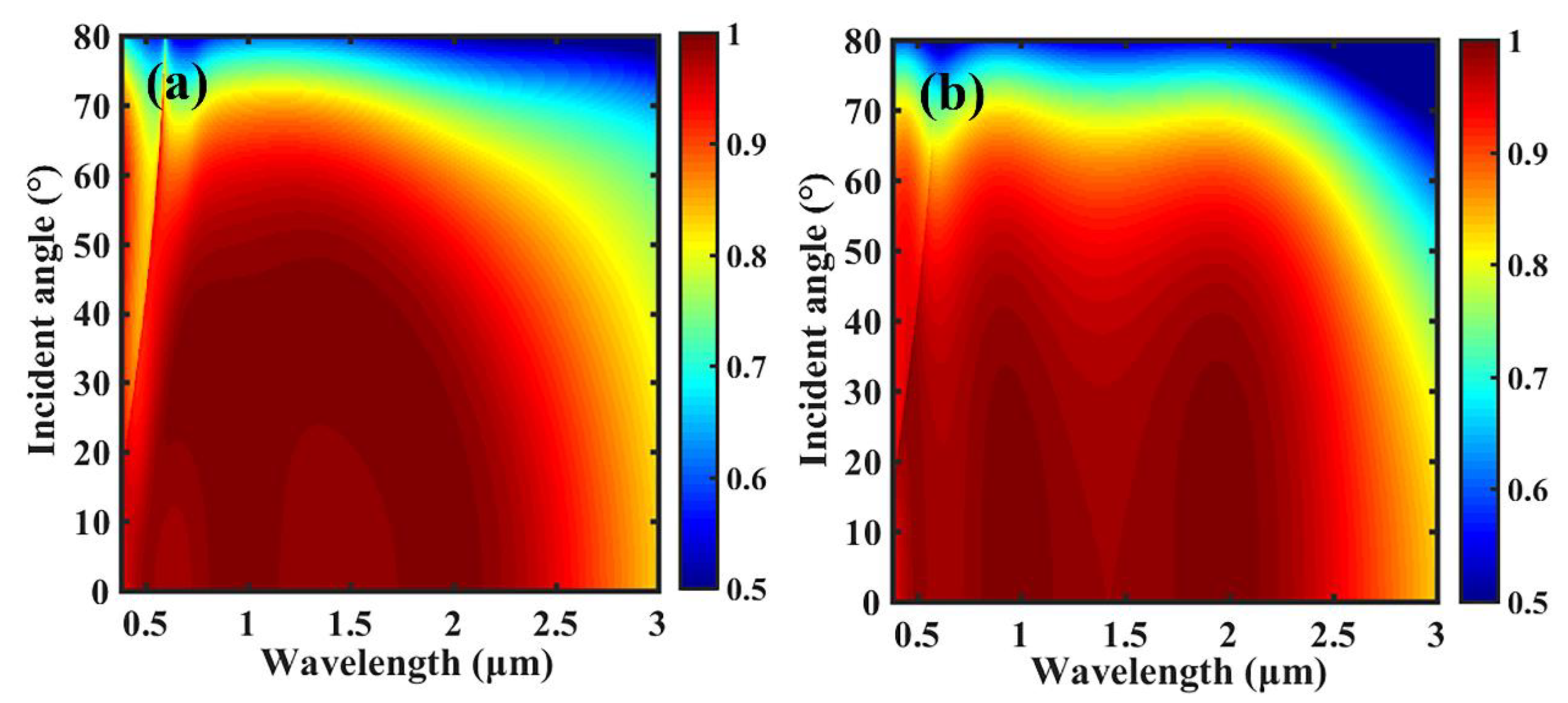
4. Results and Discussions

To further evaluate the robustness of the absorption performance of the CNA-based absorber, we first investigated the influence of the height and diameter of the top Ti nanorods on absorption spectra of the CNA-based metasurface. As indicated in Figure 5a, the absorption performance of the CNA-based metasurface is almost immune to the variation of the height of the top Ti nanorods, and ultralbroadband absorption can be maintained unless the top Ti nanorods are totally eliminated. As seen in Figure 5b, the overall absorption of the CNA-based metasurface can be improved with the increase of the diameter of the top Ti nanorods, and the absorption performance will be saturated as D1 = 140 nm. Increasing the diameter of the top Ti nanorods will deteriorate the absorption performance of the structure as D1 > 140 nm, and the ultrabroadband absorption performance will be cancelled as D1 = D2 = 276 nm. However, excellent absorption performance of the structure can be maintained around D1 = 100 nm even when the diameter of the top Ti nanorods has been changed dramatically.
Figure 6 shows the influence of the buffer layer on absorption performance of the CNA-based metasurface. As shown in Figure 6a, the variation of tb almost does not change the absorption performance of the structure in the longer wavelength region, but the absorption in the shorter wavelength region will be slightly altered as tb is varied. Because the absorption enhancement of the longer wavelength primarily results from the PRC mode confined between the multilayer nanorods, the absorption performance is almost independent of tb. However, the variation of tb will affect the electromagnetic coupling between the top Ti nanorods and the multilayer nanorods, and the LSP mode confined by the top Ti nanorods will be slightly changed as well. As a result, the corresponding absorption will be slightly altered as tb is varied. In Figure 6b, it can be seen that the absorption of the CNA-based metasurface is insensitive to the variation of the refractive index of the buffer layer. Here, although five arbitrary dielectric materials, such as MgF2 (n = 1.38), SiO2 (n = 1.47), Al2O3 (n = 1.77), HfO2 (n = 1.97) and TiO2 (n = 2.50), are used as the buffer layer, the ultrabroadband absorption of the structure can be maintained in the whole wavelength region. As can be seen in Figure 3, because the electric field related to absorption wavelength is highly confined by the top Ti nanorods and the cavities of the adjacent multilayer nanorods, the variation of the refractive index of the buffer layer has little influence on the absorption performance of the CNA-based metasurface. This will facilitate the selection of materials in application.
Figure 7 shows the influence of the multilayer nanorods on absorption performance of the CNA-based metasurface. As indicated in Figure 7a, the absorption of the structure can be enhanced with the increase of D2 in the longer wavelength region, and its absorption will be saturated as D2 = 276 nm. In particular, as D2 is increased to 300 nm (D2 = P), the narrow cavities that can support the PRC mode between the neighboring multilayer nanorods disappear. Thus, the absorption is reduced in the longer wavelength region. In Figure 7b, it can be seen that there is no obvious absorption enhancement for the longer wavelength as N = 1; this is because the thickness of the multilayer nanorods is too small to support the PRC mode. Perfect absorption performance of the structure can be achieved with N = 5, and further increasing N will cause a decrease of the overall absorption in the longer wavelength region. Because the increase of N will increase the overall reflection of the structure, and the absorption of the structure is reduced as well, there is a trade-off between the absorption performance and the number of the multilayer nanorods. Note the absorption mechanism of the CNA-based metasurface is different from those of HMM-based absorbers [33,34], in which the absorption is improved by increasing the number of the metal/dielectric stacks. In fact, the CNA-based metasurface required only several film stacks to achieve the ultrabroadband absorption. Thus, it is also an ultracompact absorber with a total thickness of 385 nm as N = 5.
Figure 8 shows the influence of period and material on the absorption performance of the CNA-based metasurface. As shown in Figure 8a, the absorption performance is robust to the variation of the period, and ultrabroadband features are retained even when the period is significantly altered. However, the variation of the period will change the width of the cavity between the neighboring multilayer nanorods, and the PRC mode confined in the cavity will be affected as well, thus the absorption in the longer wavelength is slightly altered as P is varied. In Figure 8b, three different metallic materials (Cr, Ni, Fe) and two different dielectric materials (MgF2, HfO2) are selected to evaluate the absorption performance of the CNA-based metasurface; the dielectric constants of Cr, Ni, and Fe were obtained from Palik [52]. As shown in Figure 8b, ultrabroadband absorption performance can be maintained even if different metal/dielectric materials are chosen with the structural parameters kept the same. Therefore, the CNA-based metasurface may provide a general architecture to realize ultrabroadband absorption with high absorption efficiency based on low-cost metallic materials.
Finally, we evaluate the angular robustness of the proposed CNA-based absorber. As shown in Figure 9, the CNA-based absorber exhibits a nearly omnidirectional absorption performance for both the TM and TE (electric field along y-axis) polarizations. For the TM polarization, ultrabroadband absorption enhancement can be kept almost the same even if the incident angle is significantly altered, and an average absorptivity of 87.6% can be achieved in the range of 0.38–2.65 μm even if the incident angle is increased to 60°. In particular, for the TE mode, the average absorptivity can be kept at 90.0% in the range of 0.38–2.65 μm as the incident angle is increased to 60°. For the TE-polarized incident wave, its tangential component of the electric field is always equal to the total electric field for different incident angles, and it has a stronger contribution to match the tangential fields at the interfaces of the CNA-based absorber compared with the TM polarization, which may be responsible for the better angular response. Since any oblique incident waves can be decomposed into TM and TE modes, the results indicate that the proposed structure can function as an omnidirectional absorber due to its high angular tolerance for both TM and TE modes in the range of 0–60°.

5. Conclusions

An ultrabroadband, omnidirectional, and polarization-insensitive absorber based on CNAs is numerically demonstrated, which consists of the top Ti nanorods and the bottom Ti/SiO2 multilayer nanorods separated by a SiO2 buffer layer. The physical mechanism for ultrabroadband absorption of the proposed absorber results from the synergistic effect of the LSP and PRC modes, which is completely different from those HMM-based absorbers associated with the slow-light mode. The CNA-based absorber requires only several film stacks, and an average absorptivity of 98.2% with RAB = 149.8% can be achieved in the 0.38–2.65 μm wavelength range. According to the impedance theory, the impedance of the structure matches well with the impedance of the free space from the visible to the near-infrared spectral range. It is remarkable that the absorption performance of the CNA-based absorber is robust to the variations of the structural parameters such as thickness and diameter of the top Ti nanorods, thickness and refractive index of the buffer layer, diameter and number of the Ti/SiO2 stacks, period, and the metal/dielectric materials. In addition, the CNA-based absorber exhibits omnidirectional independence for both TM and TE polarizations in the range of 0–60°. This design strategy and architecture may provide an alternative scheme towards ultrabroadband absorption and might find applications in photoelectric detection, optical imaging, and photovoltaic solar energy conversion.

Author Contributions

In this work, X.W. and T.S. conceived the idea, simulated the design, optimized the structural parameters, and drafted the manuscript; H.Q. and G.L. discussed the idea and checked the data; X.Y. and Y.W. checked the manuscript. All authors have read and agreed to the published version of the manuscript.

Funding

This research work was supported by the National Natural Science Foundation of China (Grant No. 61975153), and Fundamental Research Funds for the Central Universities (Grant No. JUSRP21935).

Conflicts of Interest

The authors declare no conflict of interest.

References

  1. Yong, Z.D.; Zhang, S.L.; Gong, C.S.; He, S.L. Narrow band perfect absorber for maximum localized magnetic and electric field enhancement and sensing applications. Sci. Rep. 2016, 6, 24063. [Google Scholar] [CrossRef] [PubMed] [Green Version]
  2. Meng, L.J.; Zhao, D.; Ruan, Z.C.; Li, Q.; Yang, Y.Q.; Qiu, M. Optimized grating as an ultra-narrow band absorber or plasmonic sensor. Opt. Lett. 2014, 39, 1137. [Google Scholar] [CrossRef] [PubMed]
  3. Yang, Z.Q.; Du, K.; Lu, F.F.; Pang, Y.; Hua, S.J.; Gan, X.T.; Zhang, W.D.; Chua, S.J.; Mei, T. Silica nanocone array as a template for fabricating a plasmon induced hot electron photodetector. Photonics Res. 2019, 7, 294–299. [Google Scholar] [CrossRef]
  4. Gong, Y.k.; Wang, Z.B.; Li, K.; Uggalla, L.; Huang, J.G.; Copner, N.; Zhou, Y.; Qiao, D.; Zhu, J.Y. Highly efficient and broadband mid-infrared metamaterial thermal emitter for optical gas sensing. Opt. Lett. 2017, 42, 4537–4540. [Google Scholar] [CrossRef]
  5. Mason, J.A.; Smith, S.; Wasserman, D. Strong absorption and selective thermal emission from a midinfrared metamaterial. Appl. Phys. Lett. 2011, 98, 241105. [Google Scholar] [CrossRef] [Green Version]
  6. Vora, A.; Gwamuri, J.; Pala, N.; Kulkarni, A.; Pearce, J.M.; Güney, D.Ö. Exchanging ohmic losses in metamaterial absorbers with useful optical absorption for photovoltaics. Sci. Rep. 2014, 4, 4901. [Google Scholar] [CrossRef] [Green Version]
  7. Hägglund, C.; Zeltzer, G.; Ruiz, R.; Wangperawong, A.; Roelofs, K.E.; Bent, S.F. Strong coupling of plasmon and nanocavity modes for dual-band, near-perfect absorbers and ultrathin photovoltaics. ACS Photonics 2016, 3, 456–463. [Google Scholar] [CrossRef] [Green Version]
  8. Landy, N.I.; Sajuyigbe, S.; Mock, J.J.; Smith, D.R.; Padilla, W.J. Perfect metamaterial absorber. Phys. Rev. Lett. 2008, 100, 207402. [Google Scholar] [CrossRef]
  9. Lee, B.J.; Wang, L.P.; Zhang, Z.M. Coherent thermal emission by excitation of magnetic polaritons between periodic strips and a metallic film. Opt. Express 2008, 16, 11328–11336. [Google Scholar] [CrossRef]
  10. Liao, Y.L.; Zhao, Y. Absorption manipulation in a narrowband infrared absorber based on the hybridization of gap plasmon and Fabry-Perot resonance. Plasmonics 2015, 10, 1219–1223. [Google Scholar] [CrossRef]
  11. Hao, J.M.; Wang, J.; Liu, X.L.; Padilla, W.J.; Zhou, L.; Qiu, M. High performance optical absorber based on a plasmonic metamaterial. Appl. Phys. Lett. 2010, 96, 251104. [Google Scholar] [CrossRef]
  12. Hao, J.M.; Zhou, L.; Qiu, M. Nearly total absorption of light and heat generation by plasmonicmetamaterials. Phys. Rev. B 2011, 83, 165107. [Google Scholar] [CrossRef]
  13. Fang, Z.Y.; Zhen, Y.R.; Fan, L.R.; Zhu, X.; Nordlander, P. Tunable wide-angle plasmonic perfect absorber at visible frequencies. Phys. Rev. B 2012, 85, 245401. [Google Scholar] [CrossRef]
  14. Liu, N.; Mesch, M.; Weiss, T.; Hentschel, M.; Giessen, H. Infrared perfect absorber and its application as plasmonic sensor. Nano Lett. 2010, 10, 2342–2348. [Google Scholar] [CrossRef]
  15. Cheng, H.; Chen, S.Q.; Yang, H.F.; Li, J.J.; An, X.; Gu, C.Z.; Tian, J.G. A polarization insensitive and wide-angle dual-band nearly perfect absorber in the infrared regime. J. Opt. 2012, 14, 085102. [Google Scholar] [CrossRef]
  16. Wu, C.H.; Shvets, G. Design of metamaterial surfaces with broad-band absorbance. Opt. Lett. 2012, 37, 308–310. [Google Scholar] [CrossRef] [Green Version]
  17. Cui, Y.X.; Xu, J.; Fung, K.H.; Jin, Y.; Kumar, A.; He, S.L.; Fang, N.X. A thin film broadband absorber based on multi-sized nanoantennas. Appl. Phys. Lett. 2011, 99, 253101. [Google Scholar] [CrossRef]
  18. Hu, C.G.; Liu, L.Y.; Zhao, Z.Y.; Chen, X.N.; Luo, X.G. Mixed plasmons coupling for expanding the bandwidth of near-perfect absorption at visible frequencies. Opt. Express 2009, 17, 16745–16749. [Google Scholar] [CrossRef]
  19. Hendrickson, J.; Guo, J.P.; Zhang, B.Y.; Buchwald, W.; Soref, R. Wideband perfect light absorber at midwave infrared using multiplexed metal structures. Opt. Lett. 2012, 37, 371–373. [Google Scholar] [CrossRef]
  20. Wang, H.; Wang, L.P. Perfect selective metamaterial solar absorbers. Opt. Express 2013, 21, A1078–A1093. [Google Scholar] [CrossRef]
  21. Lefebvre, A.; Costantini, D.; Doyen, I.; Levesque, Q.; Lorent, E.; Jacolin, D.; Greffet, J.J.; Boutami, S.; Benisty, H. CMOS compatible metal-insulator-metal plasmonic perfect absorbers. Opt. Mater. Express 2016, 6, 2389–2396. [Google Scholar] [CrossRef] [Green Version]
  22. Cheng, C.W.; Abbas, M.N.; Chiu, C.W.; Lai, K.T.; Shih, M.H.; Chang, Y.C. Wide-angle polarization independent infrared broadband absorbers based on metallic multisized disk arrays. Opt. Express 2012, 20, 10376–10381. [Google Scholar] [CrossRef]
  23. Liu, Z.Q.; Liu, G.Q.; Liu, X.S.; Wang, Y.; Fu, G.L. Titanium resonators based ultra-broadband perfect light absorber. Opt. Mater. 2018, 83, 118–123. [Google Scholar] [CrossRef]
  24. Liu, X.L.; Tyler, T.; Starr, T.; Starr, A.F.; Jokerst, N.M.; Padilla, W.J. Taming the blackbody with metamaterials. Phys. Rev. Lett. 2011, 107, 045901. [Google Scholar] [CrossRef] [Green Version]
  25. Li, Z.G.; Stan, L.; Czaplewski, D.A.; Yang, X.D.; Gao, J. Wavelength-selective mid-infrared metamaterial absorbers with multiple tungsten cross resonators. Opt. Express 2018, 26, 5616–5631. [Google Scholar] [CrossRef] [Green Version]
  26. Ghobadi, A.; Dereshgi, S.A.; Hajian, H.; Bozok, B.; Butun, B.; Ozbay, E. Ultra-broadband, wide angle absorber utilizing metal insulator multilayers stack with a multi-thickness metal surface texture. Sci. Rep. 2017, 7, 4755. [Google Scholar] [CrossRef]
  27. Sang, T.; Gao, J.; Yin, X.; Qi, H.L.; Wang, L.; Jiao, H.F. Angle-insensitive broadband absorption enhancement of graphene using a multi-grooved metasurface. Nanoscale Res. Lett. 2019, 14, 105. [Google Scholar] [CrossRef] [Green Version]
  28. Poddubny, A.; Iorsh, I.; Belov, P.; Kivshar, Y. Hyperbolic metamaterials. Nat. Photonics 2013, 7, 948. [Google Scholar] [CrossRef]
  29. Zhukovsky, S.V.; Kidwai, O.; Sipe, J.E. Physical nature of volume plasmonpolaritons in hyperbolic metamaterials. Opt. Express 2013, 21, 14982–14987. [Google Scholar] [CrossRef] [Green Version]
  30. Shekhar, P.; Atkinson, J.; Jacob, Z. Hyperbolic metamaterials: Fundamentals and applications. Nano Converg. 2014, 1, 14. [Google Scholar] [CrossRef]
  31. Xiang, Y.J.; Dai, X.Y.; Guo, J.; Zhang, H.; Wen, S.C.; Tang, D.Y. Critical coupling with graphene-based hyperbolic metamaterials. Sci. Rep. 2014, 4, 5483. [Google Scholar] [CrossRef] [Green Version]
  32. Sreekanth, K.V.; Alapan, Y.; Elkabbash, M.; Ilker, E.; Hinczewski, M.; Gurkan, U.A.; Luca, A.D.; Strangi, G. Extreme sensitivity biosensing platform based on hyperbolic metamaterials. Nat. Mater. 2016, 15, 621–627. [Google Scholar] [CrossRef] [PubMed] [Green Version]
  33. Qi, H.L.; Sang, T.; Wang, L.; Yin, X.; Wang, J.C.; Wang, Y.K. Dual-band light absorption enhancement in hyperbolic rectangular array. Appl. Sci. 2019, 9, 2011. [Google Scholar] [CrossRef] [Green Version]
  34. Cao, S.; Yu, W.; Wang, T.; Xu, Z.; Wang, C.; Fu, Y.; Liu, Y. Two-dimensional subwavelength meta-nanopillar array for efficient visible light absorption. Appl. Phys. Lett. 2013, 102, 161109. [Google Scholar] [CrossRef]
  35. Cui, Y.X.; Fung, K.H.; Xu, J.; Ma, H.; Jin, Y.; He, S.L.; Fang, N.X. Ultrabroadband light absorption by a sawtooth anisotropic metamaterial slab. Nano Lett. 2012, 12, 1443–1447. [Google Scholar] [CrossRef] [Green Version]
  36. Hu, H.F.; Ji, D.X.; Zeng, X.; Liu, K.; Gan, Q.Q. Rainbow trapping in hyperbolic metamaterial waveguide. Sci. Rep. 2013, 3, 1249. [Google Scholar] [CrossRef]
  37. Ji, D.X.; Song, H.M.; Zeng, X.; Hu, H.F.; Liu, K.; Zhang, N.; Gan, Q.Q. Broadband absorption engineering of hyperbolic metafilm patterns. Sci. Rep. 2014, 4, 4498. [Google Scholar] [CrossRef] [Green Version]
  38. Zhou, J.; Kaplan, A.F.; Chen, L.; Guo, L.J. Experiment and theory of the broadband absorption by a tapered hyperbolic metamaterial array. ACS Photonics 2014, 1, 618–624. [Google Scholar] [CrossRef]
  39. Wu, J. Broadband light absorption by tapered metal-dielectric multilayered grating structures. Opt. Commun. 2016, 365, 93–98. [Google Scholar] [CrossRef]
  40. Li, Y.L.; An, B.; Li, L.Z.; Gao, J. Broadband LWIR and MWIR absorber by trapezoid multilayered grating and SiO2 hybrid structure. Opt. Quant. Electron. 2018, 50, 459. [Google Scholar] [CrossRef]
  41. Long, C.; Yin, S.; Wang, W.; Li, W.; Zhu, J.F.; Guan, J.G. Broadening the absorption bandwidth of metamaterial absorbers by transverse magnetic harmonics of 210 mode. Sci. Rep. 2016, 6, 21431. [Google Scholar] [CrossRef] [Green Version]
  42. Liang, Q.Q.; Wang, T.S.; Lu, Z.W.; Sun, Q.; Fu, Y.Q.; Yu, W.X. Metamaterial-based two dimensional plasmonic subwavelength structures offer the broadest waveband light harvesting. Adv. Opt. Mater. 2013, 1, 43–49. [Google Scholar] [CrossRef]
  43. Ding, F.; Jin, Y.; Li, B.R.; Cheng, H.; Mo, L.; He, S.L. Ultrabroadband strong light absorption based on thin multilayered metamaterials. Laser Photonics Rev. 2014, 8, 946–953. [Google Scholar] [CrossRef]
  44. Lin, Y.Y.; Cui, Y.X.; Ding, F.; Fung, K.H.; Ji, T.; Li, D.D.; Hao, Y.Y. Tungsten based anisotropic metamaterial as an ultra-broadband absorber. Opt. Mater. Express 2017, 7, 606–617. [Google Scholar] [CrossRef] [Green Version]
  45. Hu, S.; Yang, H.L.; Huang, X.J.; Liu, D. Metamaterial-based frustum of cones array nanostructure for efficient absorber in the solar spectral band. Appl. Phys. A 2014, 117, 1375–1380. [Google Scholar] [CrossRef]
  46. Hoa, N.T.Q.; Tung, P.D.; Lam, P.H.; Dung, N.D.; Quang, N.H. Numerical study of an ultrabroadband, wide-angle, polarization-insensitivity metamaterial absorber in the visible region. J. Electron. Mater. 2018, 47, 2634–2639. [Google Scholar] [CrossRef]
  47. Hu, S.; Yang, S.Y.; Liu, Z.; Quan, B.G.; Li, J.J.; Gu, C.Z. Broadband and polarization-insensitive absorption based on a set of multisized Fabry–Perot-like resonators. J. Phys. Chem. C 2019, 123, 13856–13862. [Google Scholar] [CrossRef]
  48. Yin, X.; Chen, L.; Li, X. Ultra-broadband super light absorber based on multi-sized tapered hyperbolic metamaterial waveguide arrays. J. Lightwave Technol. 2015, 33, 3704–3710. [Google Scholar] [CrossRef]
  49. Yin, X.; Long, C.; Li, J.H.; Zhu, H.; Chen, L.; Guan, J.G.; Li, X. Ultra-wideband microwave absorber by connecting multiple absorption bands of two different-sized hyperbolic metamaterial waveguide arrays. Sci. Rep. 2015, 5, 15367. [Google Scholar] [CrossRef] [Green Version]
  50. Tsakmakidis, K.L.; Boardman, A.D.; Hess, O. ‘Trapped rainbow’ storage of light in metamaterials. Nature 2007, 450, 397–401. [Google Scholar] [CrossRef]
  51. Smolyaninova, V.N.; Smolyaninov, I.I.; Kildishev, A.V.; Shalaev, V.M. Experimental observation of the trapped rainbow. Appl. Phys. Lett. 2010, 96, 211121. [Google Scholar] [CrossRef] [Green Version]
  52. Palik, E.D. Handbook of Optical Constants of Solids; Academic Press: New York, NY, USA, 1998. [Google Scholar]
  53. Zhou, J.Y.; Sang, T.; Li, J.L.; Wang, R.; Wang, L.; Wang, B.X.; Wang, Y.K. Modal analysis on resonant excitation of two-dimensional waveguide grating filters. Opt. Commun. 2017, 405, 350–354. [Google Scholar] [CrossRef]
  54. Wu, J. Absorption enhancement in thin-film solar cells based on periodically chirped structure. Sol. Energy 2018, 165, 85–89. [Google Scholar] [CrossRef]
  55. Deng, G.S.; Song, X.L.; Dereshgi, S.A.; Xu, H.Q.; Aydin, K. Tunable multi-wavelength absorption in mid-IR region based on a hybrid patterned graphene-hBN structure. Opt. Express 2019, 27, 23576–23584. [Google Scholar] [CrossRef]
  56. Hoa, N.T.Q.; Lam, P.H.; Tung, P.D.; Tuan, T.S.; Nguyen, H. Numerical study of a wide-angle and polarization-insensitive ultrabroadband metamaterial absorber in visible and near-infrared region. IEEE Photonics J. 2019, 11, 4600208. [Google Scholar] [CrossRef]
  57. He, X.J.; Yan, S.T.; Lu, G.J.; Zhang, Q.F.; Wu, F.M.; Jiang, J.X. An ultra-broadband polarization-independent perfect absorber for solar spectrum. RSC Adv. 2015, 5, 61955–61959. [Google Scholar] [CrossRef]
  58. Krenn, J.R.; Weeber, J.C.; Dereux, A.; Bourillot, E.; Goudonnet, J.P. Direct observation of localized surface plasmon coupling. Phys. Rev. B 1999, 60, 5029–5033. [Google Scholar] [CrossRef]
  59. Ghobadi, A.; Hajian, H.; Gokbayrak, M.; Dereshgi, S.A.; Toprak, A.; Butun, B.; Ozbay, E. Visible light nearly perfect absorber: An optimum unit cell arrangement for near absolute polarization insensitivity. Opt. Express 2017, 25, 27624–27634. [Google Scholar] [CrossRef]
  60. Chanda, D.; Shigeta, K.; Truong, T.; Lui, E.; Mihi, A.; Schulmerich, M.; Braun, P.V.; Bhargava, R.; Rogers, J.A. Coupling of plasmonic and optical cavity modes in quasi-three-dimensional plasmonic crystals. Nat. Commun. 2011, 2, 479. [Google Scholar] [CrossRef] [Green Version]
  61. Song, H.J.; Zang, J.X.; Fei, G.T.; Wang, J.F.; Jiang, K.; Wang, P.; Lu, Y.H.; Iorsh, I.; Xu, W.; Jia, J.H.; et al. Near-field coupling and resonant cavity modes in plasmonicnanorodmetamaterials. Nanotechnology 2016, 27, 415708. [Google Scholar] [CrossRef] [Green Version]
  62. Wang, J.F.; Zhang, C.; Zhang, J.X.; Song, H.J.; Wang, P.; Lu, Y.H.; Fei, G.T.; Xu, W.; Xu, W.; Zhang, L.D.; et al. Hybrid plasmonic cavity modes in arrays of gold nanotubes. Adv. Opt. Mater. 2017, 5, 1600731. [Google Scholar] [CrossRef] [Green Version]
  63. Smith, D.R.; Vier, D.C.; Koschny, T.; Soukoulis, C.M. Electromagnetic parameter retrieval from inhomogeneous metamaterials. Phys. Rev. E 2005, 71, 036617. [Google Scholar] [CrossRef] [Green Version]
  64. Yin, X.; Sang, T.; Qi, H.L.; Li, G.Q.; Wang, X.; Wang, J.C.; Wang, Y.K. Symmetry-broken square silicon patches for ultra-narrowband light absorption. Sci. Rep. 2019, 9, 17477. [Google Scholar] [CrossRef]
Figure 1. (a) Sketch map of the CNA-based metasurface for ultrabroadband light absorption. (b) A unit cell of the CNA-based metasurface.
Applsci 10 03878 g001
Figure 2. Absorption performance of different CNA-based structures. The parameters are: P = 300 nm, N = 5, h = 140 nm, tb = 30 nm, tm = 10 nm, td = 33 nm, D1 = 140 nm, and D2 = 276 nm. (a) Absorption of total structure, total structure with D1 = D2 = 276 nm, and total structure without Ti rods. (b) Absorption of CNA-based absorber, and absorption distributions of different parts of the structure.
Applsci 10 03878 g002
Figure 3. Electric field and Poynting vector distributions of CNA-based absorber at three resonance absorption peaks. (a) λ = 0.524 μm; (b) λ = 1.001 μm; (c) λ = 1.952 μm. The parameters are the same as those in Figure 2b, the arrows indicate the Poynting vector direction.
Applsci 10 03878 g003
Figure 4. (a) Impedance and reflection curves of the CNA-based metasurface. (b) FDTD result and theoretical results of absorption spectral of the CNA-based metasurface.
Applsci 10 03878 g004
Figure 5. Influence of the top Ti nanorods on absorption performance of the CNA-based metasurface. Other parameters are the same as those in Figure 2b. (a) Absorption as a function of the height of the top Ti nanorods. (b) Absorption as a function of the diameter of the top Ti nanorods.
Applsci 10 03878 g005
Figure 6. Influence of buffer layer on absorption performance of the CNA-based metasurface. Other parameters are the same as those in Figure 2b. (a) Absorption as a function of the thickness of buffer layer. (b) Absorption as a function of the refractive index of buffer layer.
Applsci 10 03878 g006
Figure 7. Influence of multilayer nanorods on absorption performance of the CNA-based metasurface. Other parameters are the same as those in Figure 2b. (a) Absorption as a function of the diameter of multilayer nanorods. (b) Absorption as a function of the number of film pairs of multilayer nanorods.
Applsci 10 03878 g007
Figure 8. Influence of period and material on absorption performance of the CNA-based metasurface. Other parameters are the same as those in Figure 2b. (a) Absorption as a function of the period. (b) Absorption as a function of different metal/dielectric materials.
Applsci 10 03878 g008
Figure 9. Absorption of the CNA-based metasurface as a function of the incidence angle for (a) TM and (b) TE modes. Other parameters are the same as those in Figure 2b.
Applsci 10 03878 g009

