Article

Hybrid Resonant Converter with Three Half-Bridge Legs for Wide Voltage Operation

Department of Electrical Engineering, National Yunlin University of Science and Technology, Yunlin 640, Taiwan
*
Author to whom correspondence should be addressed.
Appl. Sci. 2020, 10(1), 310; https://doi.org/10.3390/app10010310
Submission received: 13 November 2019 / Revised: 27 December 2019 / Accepted: 30 December 2019 / Published: 31 December 2019
(This article belongs to the Special Issue Resonant Converter in Power Electronics Technology)

Abstract

:
This paper studied a hybrid resonant converter with three half bridge legs for wide input voltage operation. Compared to the conventional resonant converters with narrow voltage operation, the presented converter can achieve wider voltage operation. On the basis of the proper switching status of power switches, the developed converter can operate at half-bridge resonant circuit under high input voltage range and the other two full-bridge resonant circuits under medium and low input voltage ranges. Each resonant circuit has a 2:1 (Vin,max = 2Vin,min) input voltage operation range. Therefore, the developed converter can achieve an 8:1 (Vin,max = 8Vin,min) wide voltage operation. The main advantage of the studied converter is the single-stage direct current (DC)/DC power conversion instead of the two-stage power conversion to achieve wide voltage operation. Because the equivalent resonant tank of the adopted converter is controlled by frequency modulation, the soft switching operation on power switches or rectifier diodes can be realized to improve circuit efficiency. The performance of the proposed circuit was confirmed and verified by experiments with a laboratory circuit.

1. Introduction

Power electronic converters with high efficiency are developed for consumer electronics, battery chargers, telecommunication power units, direct current (DC) nano-grid power conversions, internet of things (IOT) power units, and renewable energy conversions. Soft switching techniques for flyback circuits, full bridge converters, and half bridge converters [1,2,3,4,5,6,7] have been developed to improve the converter efficiency and eliminate the switching losses. Phase-shift pulse-width modulation (PSPWM) full bridge converter [1,2] uses the phase angle control between the lagging-leg switches and leading-leg switches to control the load voltage and also achieve soft switching operation. However, the lagging-leg switches are hard switching operation at the light load. The high circulating current loss at low duty cycle case is the other drawback. Soft switching flybacks have been discussed in [3,4] for low power applications. Active clamp converter was discussed in [5] to reduce voltage spike on power switches by using active clamp and switch. However, the rectifier diodes have unbalanced voltage and current stresses on the output side. Resonant converters discussed in [6,7,8] can achieve low switching losses on power semiconductors. However, the output or input voltage range of the resonant converter is limited due to its low voltage gain of the series resonant circuit characteristics.
For solar photovoltaic or fuel cell systems [9,10,11,12,13], the output voltage of a solar panel depends on the geographical location and solar intensity. Therefore, the output voltage range of solar panel is wide variation. Power converters with wide input voltage operation have been discussed and developed in [9,10,11,12] for fuel cell and solar power converters with the series or parallel connected structure to extend the input voltage range. Full bridge resonant converter with one alternating current (AC) switch and two isolated transformers was developed in [13] to have a wide voltage operation range (Vin,max = 4Vin,min). However, the control algorithm is much more complicated due to four equivalent sub-circuit topologies. The power converters with wide voltage operation are also demanded for the power units in the outdoor LED lighting systems, battery chargers in electric vehicles, and railway vehicles. Due to the variable parallel or series connection of several LED strings for output lighting system, the power converters with variable output voltage are normally implemented. For railway low power supplies, the input voltages of DC converters are between 24 and 110 V for the braking system, electric door system, lighting system, and motor drive controller. For electric vehicle (EV) systems, the output voltage of battery charger is variable from 210 to 450 V. Therefore, DC converters with wide voltage range output is required for EV applications. To achieve wide voltage range output, the two-stage DC converters [14,15,16] based on the non-isolated DC/DC converter in the first-stage and the isolated DC converter in the second-stage are the simplest way to accomplish wide voltage operation. The main disadvantage of the two-stage converters is low circuit efficiency. Parallel- or series-connected converters [9,17] were developed to have wide voltage operations. However, a large number of circuit components are needed in these circuit topologies. Series resonant converters published in [18,19,20,21] have a wide voltage range operation such as Vin,max = 4Vin,min or Vo,max = 4Vo,min. By the proper control of power switches, the resonant converter can be operated at the half or full bridge circuit topology. Therefore, the resonant converters with 4:1, that is, Vin,max = 4Vin,min, wide voltage range operation are achieved. However, the voltage operation range of these circuit topologies is less than 4, that is, Vin,max ≤ 4Vin,min. If the much wider voltage range is requested, such as Vin,max ≥ 4Vin,min in solar panel applications or wide voltage variation systems, then these circuit topologies cannot be operated well.
A new resonant converter with a three converter legs structure and a variable turns ratio of transformer is presented in this study, having a wide voltage range operation. On the basis of the switching status of active switches, the proposed resonant converter has three equivalent sub-circuits to implement 8:1 (Vin,max = 8Vin,min) wide voltage range operation such as 50–400 V. If Vin (input voltage) is under low voltage range from 50 to 100 V, the sub-circuit with the full bridge circuit topology and low turns ratio transformer is operated to have high voltage gain. If Vin is under medium voltage range from 100 to 200 V, then the sub-circuit with full bridge circuit topology and high turns ratio transformer is operated to decrease the voltage gain in order to control the load voltage. If Vin is under the high voltage range from 200 to 400 V, then the sub-circuit with the half bridge circuit topology and high turns ratio is operated to further reduce the voltage gain. Three equivalent sub-circuits in the proposed converter were selected by two Schmitt voltage comparators with reference input voltages at 100 and 200 V. Therefore, the half bridge circuit topology or full-bridge circuit topology with two different turns ratios can be selected on the input side to accomplish wide input voltage operation. The circuit topology and control algorithm of the presented converter are easy to implement when compared to the conventional wide voltage range converters with two-stage circuit topologies and hybrid converters in [9,10,11,12,13,14,15,16,17,18,19,20,21]. Because the resonant circuit of the presented DC converter is controlled under the frequency modulation and the input impedance of resonant tank is always at the inductive load operation, active switches are naturally turned on at zero voltage switching operation. Finally, the design procedures and experiments are presented and confirmed with a 480 W laboratory circuit.

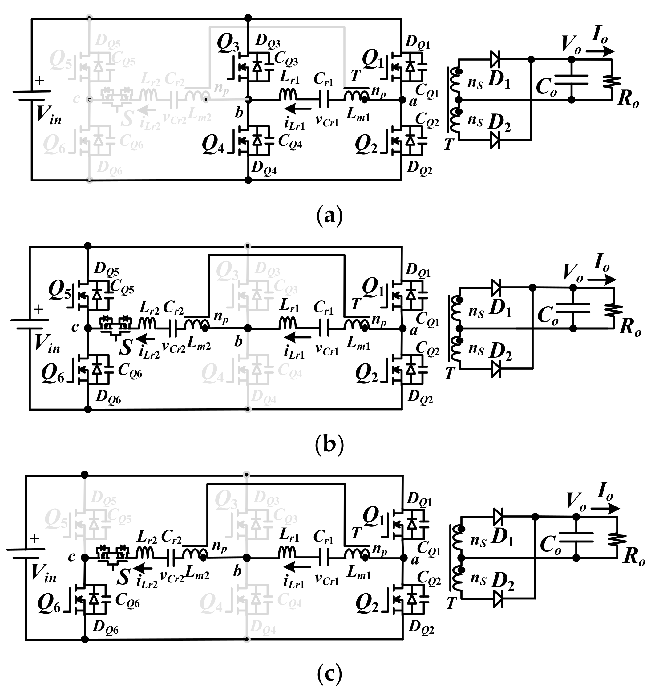
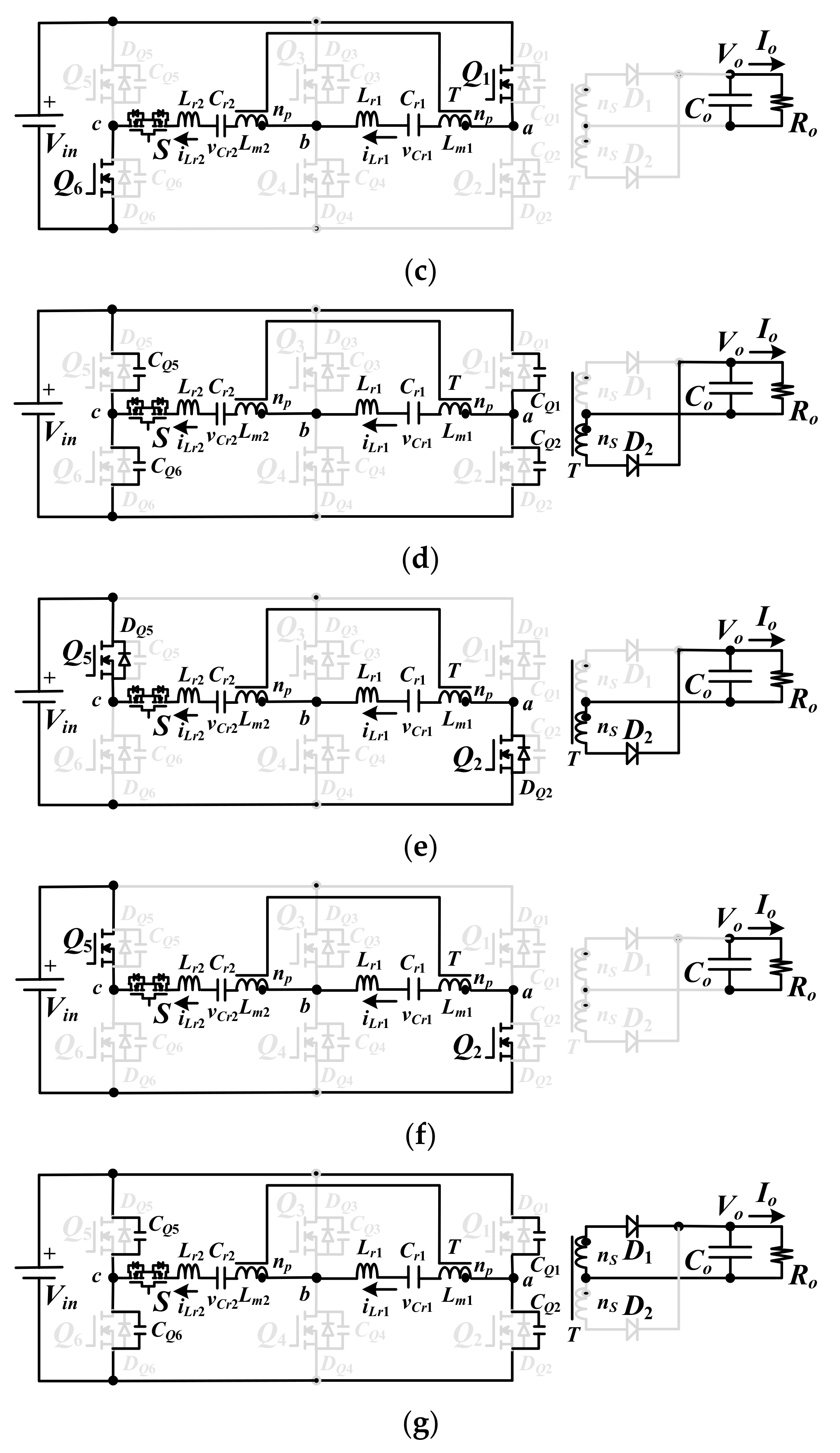
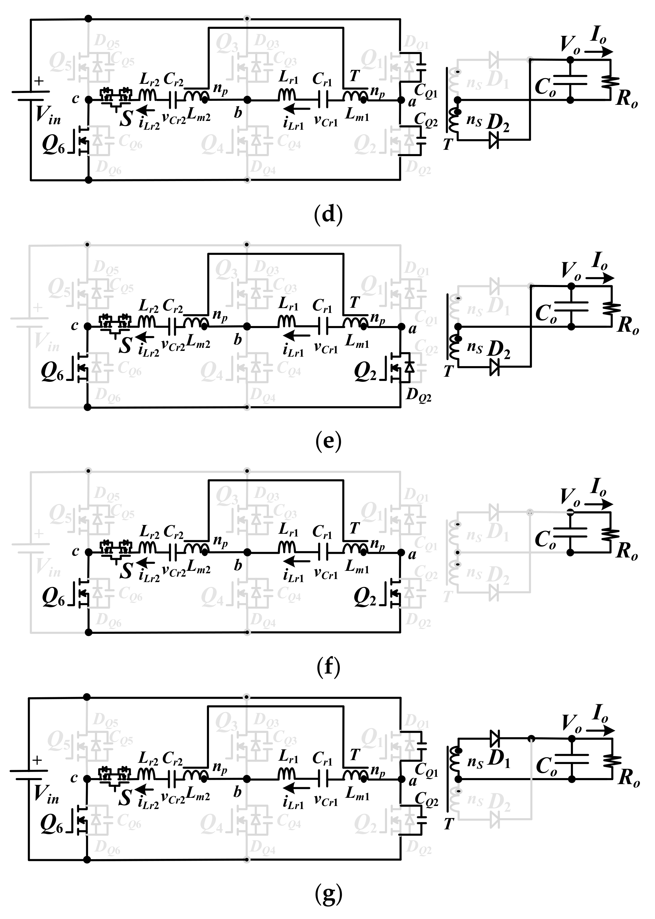
2. Circuit Structure and Principle of Operation

The circuit schematic of the developed circuit topology with wide voltage operation is shown in Figure 1. Three half-bridge legs (Q1–Q6) are used on the input side and one center-taped rectifier is used on the output side. Two resonant circuits (Lr1, Cr1, Lr2 and Cr2) with one AC power switch S are used to accomplish series resonant operation with soft switching behavior for power switches. Vin (Vo) is the input (output) voltage and Ro is the output resistor. Transformer T has two primary and secondary winding sets with np and ns winding turns, respectively. According to the switching states of Q1–Q6 and S, the developed converter can be operated under three input voltage ranges: Vin,L = Vin,max/8–Vin,max/4, Vin,M = Vin,max/4–Vin,max/2 and Vin,H = Vin,max/2–Vin,max, as shown in Figure 2. Figure 2a gives the equivalent resonant circuit if Vin is under the low voltage range Vin,L. To achieve the higher voltage gain in the proposed converter, Q5, Q6, and S are off. Only a full-bridge converter with Q1–Q4, Lr1, Cr1, and T with np primary turns are operated on the input-side. The DC voltage gain of the resonant circuit in Figure 2a is Vo/Vin,L = GL(f)ns/np, where GL(f) is the voltage gain of the proposed converter in Figure 2a. Figure 2b illustrates the equivalent circuit if Vin is under the medium voltage range Vin,M. In the medium voltage range, Q3 and Q4 are off. The resonant tank includes Lr1, Cr1, Lr2, Cr2, and transformer T with 2np primary winding turns. The series resonant frequency of this equivalent circuit is also f r = 1 / 2 π L r 1 C r 1 due to Cr1 = Cr2 and Lr1 = Lr2. The DC voltage gain of the resonant circuit shown in Figure 2b is Vo/Vin,M = GM(f)ns/(2np) due to the primary turns being 2np instead of np, where GM(f) is the voltage gain of the proposed converter in Figure 2b. Figure 2c provides the equivalent circuit if Vin is under the high voltage range Vin,H. In high voltage range, Q3, Q4, and Q5 are off and S and Q6 are on. The half-bridge resonant converter with the components Q1, Q2, Lr1, Cr1, Lr2, Cr2, and transformer T with 2np primary winding turns is operated to achieve lower voltage gain. The series resonant frequency of this equivalent circuit is f r = 1 / 2 π L r 1 C r 1 with Lr1 = Lr2 and Cr1 = Cr2. Compared to the equivalent circuit in Figure 2b, the fundamental input voltage is Vin/2 in Figure 2c instead of Vin in Figure 2b. The DC voltage gain of the equivalent circuit in Figure 2c is Vo/Vin,H = GH(f)ns/(4np), where GH(f) is the voltage gain of the proposed converter in Figure 2c. Compared to the DC voltage gain under three different input voltage gains, it observes that Vo/Vin,L = 2(Vo/Vin,M) = 4(Vo/Vin,H) if GL(f) = GM(f) = GH(f). Thus, the voltage gain of resonant circuit in Figure 2a is the largest compared to the resonant circuits in Figure 2b,c. Power switches Q1–Q6 and S can be properly controlled from three equivalent circuits, as shown in Figure 2 to have 8:1 (Vin,max = 8Vin,min) wide voltage range operation.

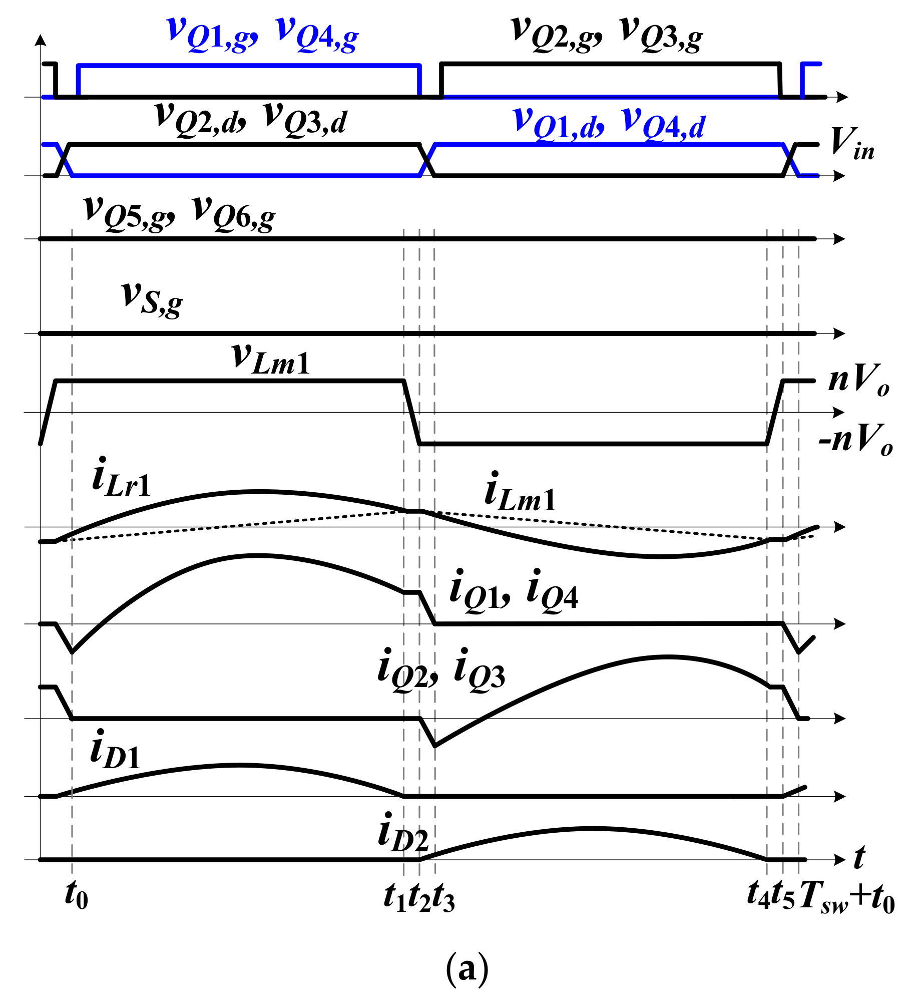
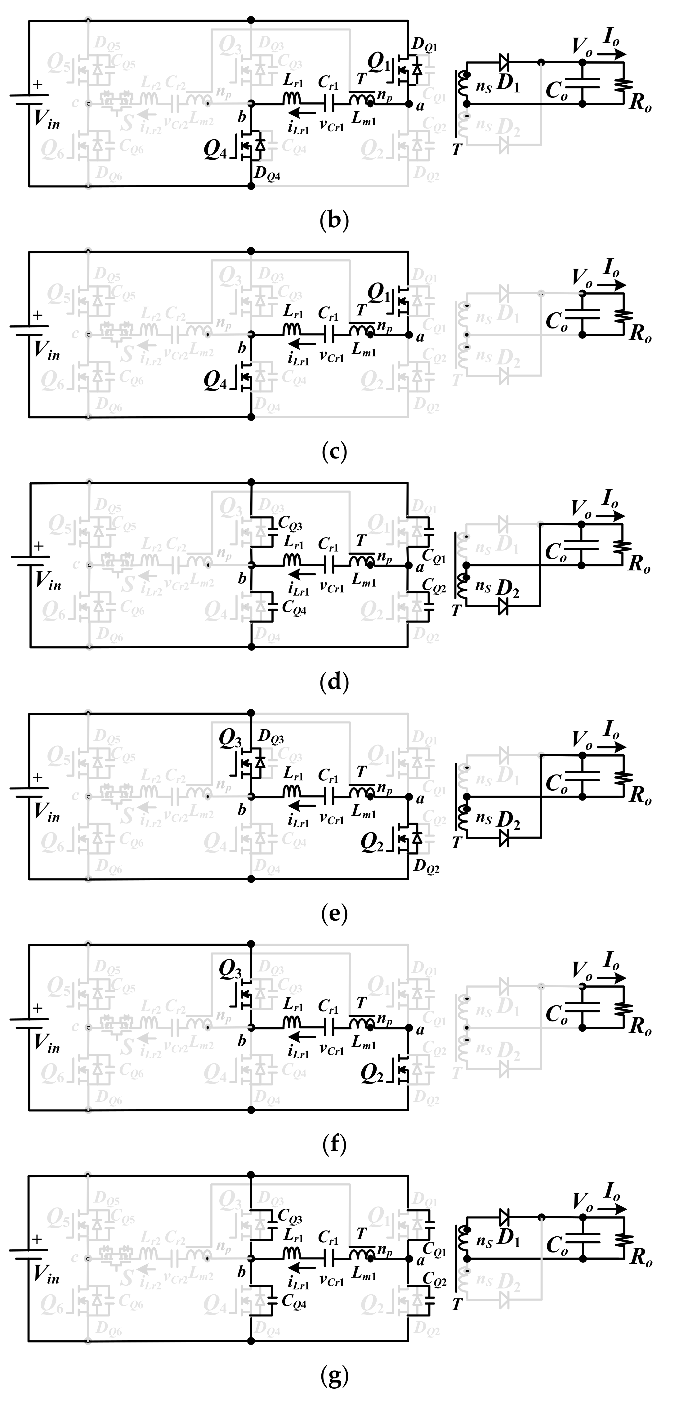
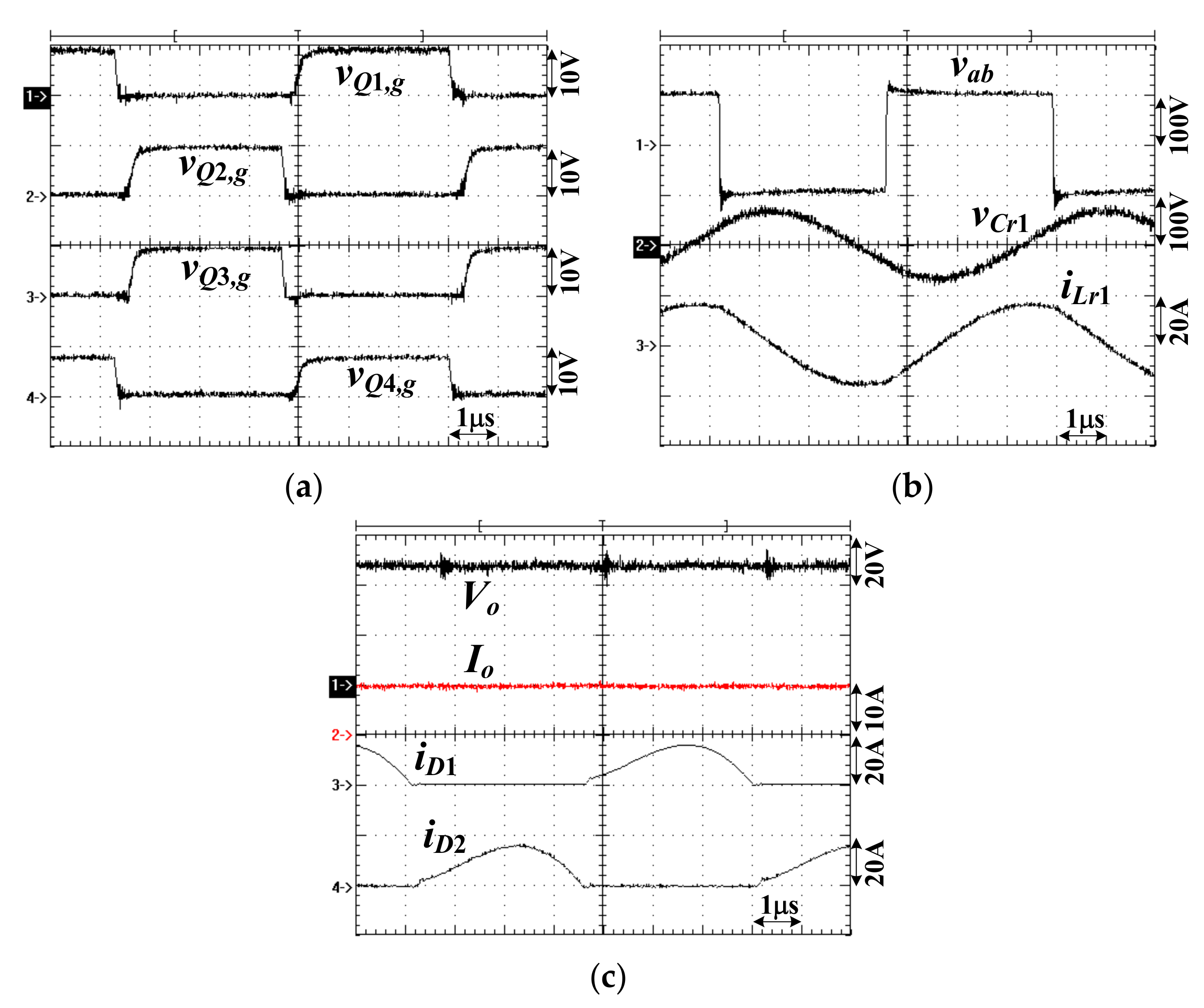
2.1. Low Input Voltage Range (S, Q5, and Q6 off, Vin,L = Vin,max/8–Vin,max/4)

If the input voltage Vin is between Vin,max/8 and Vin,max/4, S, Q5, and Q6 are turned off and only Q1–Q4 are operated to realize the high voltage gain shown in Figure 2a compared to the other two equivalent circuits (Figure 2b,c). The input-side is a full-bridge resonant converter and the output-side is a center-tapped diode rectifier. The DC voltage gain for low input voltage range is Vo/Vin,L = GL(f)ns/np. The theoretical pulse-width modulation (PWM) waveforms and the equivalent circuits for six operating states are provided in Figure 3 if fsw (switching frequency) is less than fr (series resonant frequency).
State 1 [t0t1]: At t = t0, vCQ1 = vCQ4 = 0. Then DQ1 and DQ4 are conducting due to iLr1(t0) < 0. Q1 and Q4 turn on after t0 to have soft switching operation. In this time interval, Lr and Cr are naturally resonant to deliver power to the load side. Because the diode D1 is conducting, the magnetizing voltage vLm1 = nVo, where n = np/ns, and iLm1 increases.
State2 [t1t2]: If fsw < fr, then iD1 decreases to zero at time t1 and D1 is reverse biased without the reverse recovery current. In this state, Lr1, Lm1, and Cr1 are naturally resonant with the resonant frequency f p = 1 / 2 π ( L r 1 + L m 1 ) C r 1 .
State 3 [t2t3]: At time t2, Q1 and Q4 turn off. CQ1 (CQ2) and CQ4 (CQ3) are charged (discharged) due to iLr1(t2) being positive. In this state, D2 is forward biased due to iLr1 < iLm1 and the magnetizing voltage vLm1 equals −nVo.
State4 [t3t4]: At time t3, vCQ2 = vCQ3 = 0. DQ2 and DQ3 are conducting owing to iLr1(t3) > 0. Q2 and Q3 turn on after t3 to realize the soft switching operation. In this time interval, Lr and Cr are naturally resonant to deliver power to load side. Because the diode D2 is forward biased on the secondary side, the magnetizing voltage vLm1 =nVo and iLm1 decreases.
State5 [t4t5]: At time t4, iD2 is decreased to zero so that D2 is off. In this state, Lr1, Lm1, and Cr1 are naturally resonant.
State 6 [t5Tsw + t0]: At time t5, power switches Q2 and Q3 are turned off. CQ1 (CQ2) and CQ4 (CQ3) are discharged (charged) due to iLr1(t5) is negative. In this state, D1 is forward biased owing to iLr1 > iLm1 and the magnetizing voltage vLm1 = nVo and iLm1 increases. At Tsw + t0, vCQ1 = vCQ4 = 0 and the converter goes to state 1 for the next switching period.

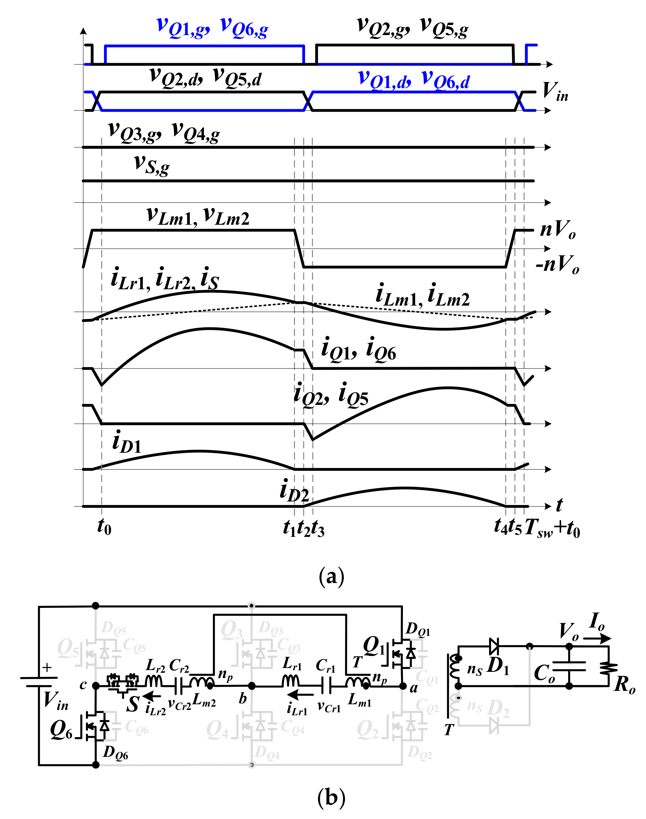
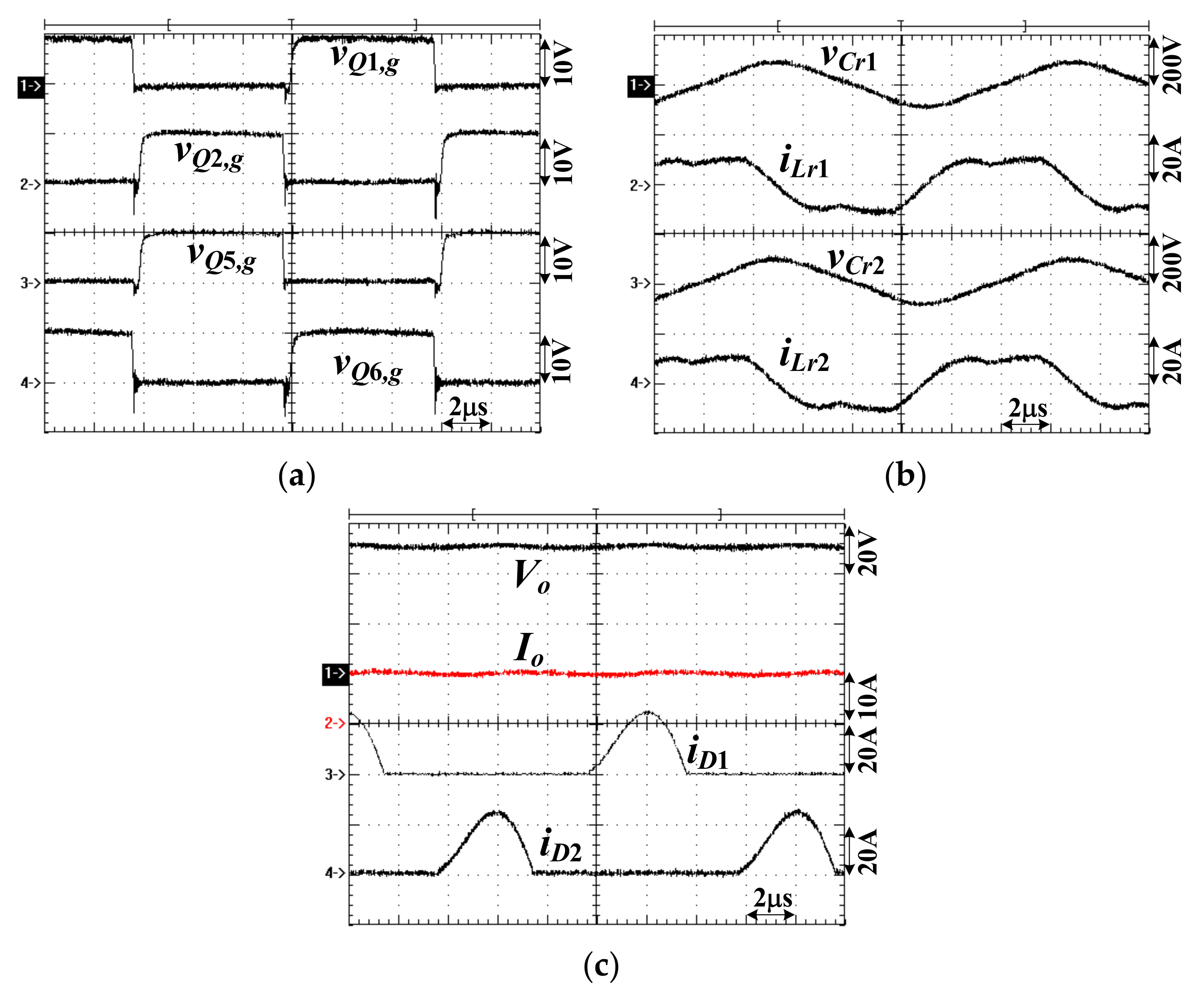
2.2. Medium Input Voltage Range (Q3 and Q4 off, Vin,M = Vin,max/4–Vin,max/2)

The proposed converter for the medium input voltage (Vin = Vin,max/4–Vin,max/2) operation is illustrated in Figure 2b. Under the medium voltage range, power switches Q3 and Q4 turn off and AC switch S is always on. The full-bridge resonant circuit is adopted on the input-side with the resonant components Lr1, Lr2, Cr1, Cr2, and transformer T with 2np primary winding turns. Because Cr1 = Cr2 and Lr1 = Lr2, the series resonant frequencies at the medium input voltage operation (Figure 2b) and the low input voltage operation (Figure 2a) are identical. The DC voltage gain for the medium voltage range is Vo/Vin,M = GM(f)ns/(2np). Comparing the DC voltage gains for low and medium voltage ranges, one can observe that Vo/Vin,L = 2(Vo/Vin,M) under GL(f) = GM(f). This means the proposed converter has less DC voltage gain at the medium input voltage range operation. The theoretical PWM waveforms and the equivalent circuits are given in Figure 4.
State 1 [t0t1]: At time t0, the capacitor voltages of vCQ1 and vCQ6 are zero. DQ1 and DQ6 are forward biased due to iLr1(t0) being negative. Q1 and Q6 can turn on after t0 to achieve zero-voltage switching. In this state, Cr1, Cr2, Lr1, and Lr2 are naturally resonant with series resonant frequency f r = 1 / 2 π L r 1 C r 1 due to Lr1 = Lr2 and Cr1 = Cr2, and the energy is transferred from Vin to Ro. Due to D1 being forward biased, the magnetizing voltage vLm1 = vLm2 = (np/ns)Vo and iLm1 and iLm2 increase.
State2 [t1t2]: If fsw (the switching frequency) < fr (series resonant frequency), then iLm1 = iLr1 and iLm2 = iLr2 at t = t1. Thus, D1 is off without reverse recovery current loss. In this state, the circuit components Cr1, Lr1, Cr2, Lr2, Lm1, and Lm2 are naturally resonant.
State 3 [t2t3]: Power switches Q1 and Q6 turn off at t = t2. CQ1 and CQ6 are charged and CQ2 and CQ5 are discharged due to iLr1(t2) > 0. Because iLr1 < iLm1 after t2, the diode D2 is forward biased.
State 4 [t3t4]:vCQ2 and vCQ5 are decreased to zero at t = t3. Because iLr1(t3) > 0, the body diodes DQ2 and DQ5 are conducting. Q2 and Q5 can be turned on after t3 to have zero-voltage switching. In this state, Cr1, Lr1, Cr2, and Lr2 are naturally resonant with series resonant frequency f r = 1 / 2 π L r 1 C r 1 and the energy is transferred from Vin to Ro. Due to D2 being forward biased, the magnetizing voltage vLm1 = vLm2 = −(np/ns)Vo and iLm1 and iLm2 decrease in state 4.
State5 [t4t5]: At time t4, iLm1 equals iLr1 and iLm2 equals iLr2. Therefore, D2 becomes off. Hence, the components Lr1, Lr2, Cr1, Cr2 Lm1, and Lm2 are naturally resonant.
State 6 [t5Tsw + t0]: Power switches Q2 and Q5 are turned off at t = t5. CQ1 (CQ2) and CQ6 (CQ5) are discharged (charged) due to iLr1(t5) < 0. Because iLr1(t5) is greater than iLm1(t5), the diode D1 is forward biased. At t = Tsw+t0, vCQ1 = vCQ6 = 0.

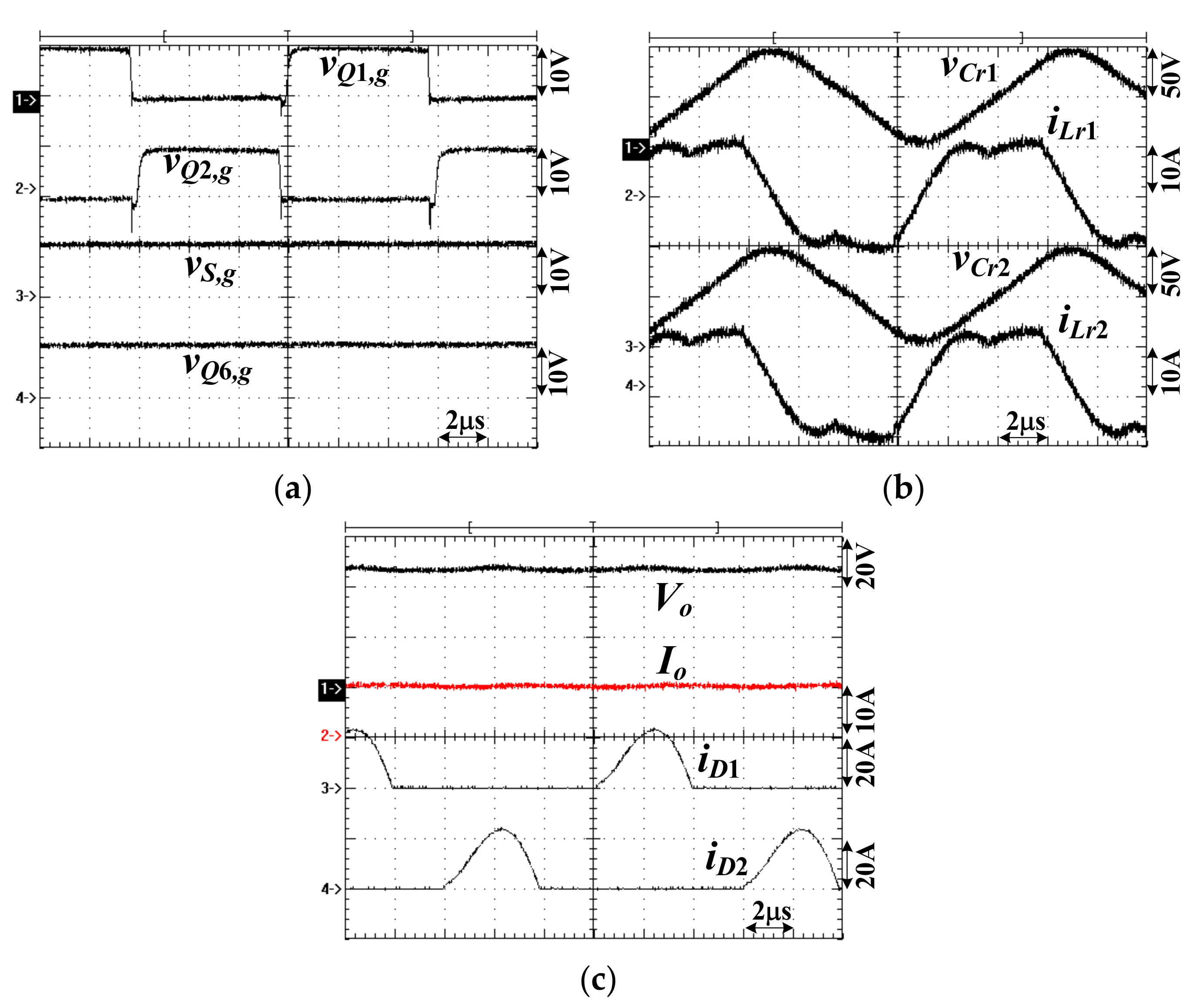
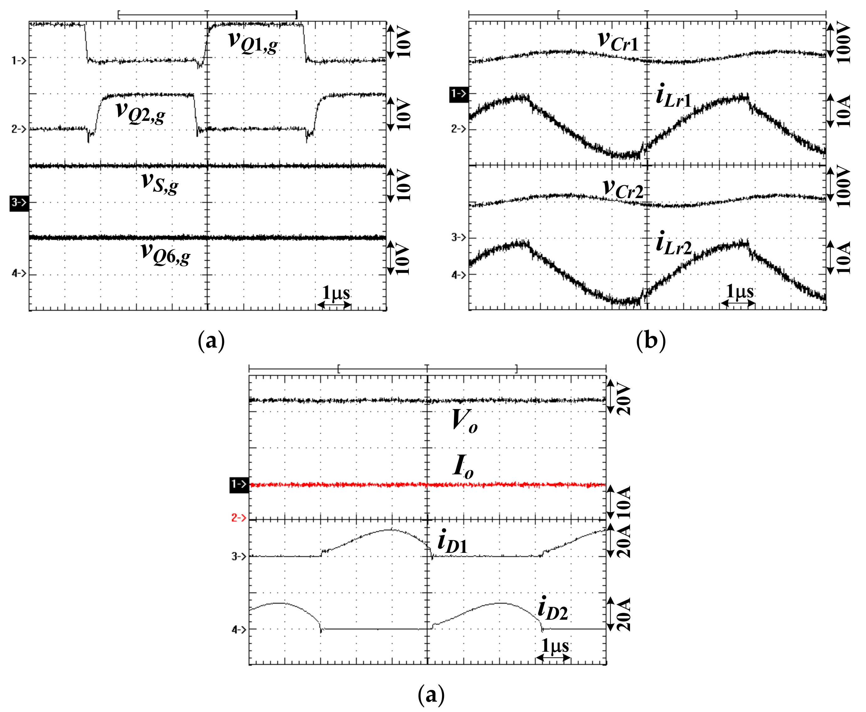
2.3. High Input Voltage Range (Q3–Q4 off, Vin,H = Vin,max/2–Vin,max)

Figure 2c shows the sub-circuit when Vin is in the high voltage range (Vin,max/2–Vin,max). Power switches Q3Q5 are turned off, and S and Q6 are always on. The half-bridge resonant circuit with the components Lr1, Lr2, Cr1, Cr2, and transformer T with 2np primary winding turns is operated to regulate the load voltage. Because Cr1 = Cr2 and Lr1 = Lr2, the series resonant frequencies for three input voltage ranges in Figure 2 are identical. The DC voltage gain in the high input voltage range is Vo/Vin,H = GH(f)ns/(4np). Comparing the DC voltage gains for three different input voltage ranges, it is observable that Vo/Vin,L = 2(Vo/Vin,M) = 4(Vo/Vin,H) if GL(f) = GM(f) = GH(f). The theoretical PWM waveforms and the equivalent circuits in a switching cycle for high input voltage range are shown in Figure 5.
State 1 [t0t1]: CQ1 is discharged to zero voltage at t = t0. Due to iLr1(t0) being negative, the body diode DQ1 is forward. Q1 can turn on after t0 to realize zero-voltage switching. Because iLr1(t0) > iLm1, D1 is conducting and vLm1 = vLm2 = nVo and iLm1 and iLm2 increase. Cr1, Cr2, Lr1 and Lr2, are resonant with resonant frequency f r = 1 / 2 π L r 1 C r 1 in this state.
State 2 [t1t2]: At time t1, iLr1 = iLm1 and iLr2 = iLm2. The rectifier diode D1 becomes off. Lm1, Lm2, Lr1, Lr2, Cr1, and Cr2 are resonant in this state.
State 3 [t2t3]: Q1 is turned off at t = t2. Due to iLr1 being positive, CQ1 (CQ2) is charged (discharged). The rectifier diode D2 is forward biased due to iLr1(t2) < iLm1(t2).
State4 [t3t4]: vCQ2 = 0 at t = t3. Owing to iLr1(t3) being positive, the body diode DQ2 is forward. Power switch Q2 can turn on after t3 to achieve zero-voltage switching. D2 is conducting owing to iLr1(t3) < iLm1(t3). Thus, vLm1 = vLm2 = −nVo and iLm1 and iLm2 decrease. Cr1, Cr2, Lr1, and Lr2 are resonant in this state.
State5 [t4t5]: At t = t4, iLr1 equals iLm1 and iLr2 equals iLm2. Then, the rectifier diode D2 becomes off. In this time interval, Lm1, Lm2, Lr1, Lr2, Cr1, and Cr2 are resonant.
State 6 [t5Tsw + t0]: Q2 turns off at t5. Because iLr1 is negative, CQ1 is discharged and CQ2 is charged. Due to iLr1(t5) > iLm1(t5), the rectifier diode D1 is forward biased. At time Tsw + t0, CQ1 is discharged to zero voltage.

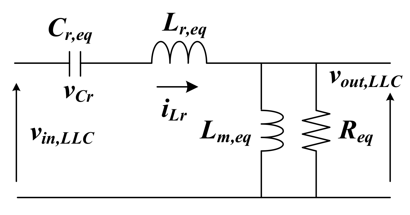
3. Circuit Characteristics

The presented circuit is controlled by frequency modulation. The input voltage Vin has a variation between 50 and 400 V and the output voltage Vo is regulated at 48 V. The fundamental harmonic analysis (FHA) proposed by [22] is selected to calculate the voltage transfer function in the proposed converter by frequency modulation. When 50 V ≤ Vin < 100 V (low voltage range), only Q1Q4 are operated (Figure 2a) to achieve high voltage gain. The square voltage waveform with voltage values of ±Vin is obtained on the leg voltage vab. If 100 V ≤ Vin < 200 V (medium voltage range), then only power switches Q1, Q2, Q5, and Q6 are controlled to control load voltage, and AC switch S is always on (Figure 2b). The square waveform with voltage values of ±Vin is obtained on the leg voltage vac. If 200 V ≤ Vin ≤ 400 V (high voltage range), then only Q1 and Q2 are operated to control the load voltage, and switches S and Q6 are always on (Figure 2c). The square waveform with voltage values of 0 and Vin is obtained on the leg voltage vac. The fundamental root mean square (rms) values of the leg voltages vab,rms (in the low voltage range) and vac,rms (in the medium and high voltage ranges) are calculated as:
v a b , r m s = 2 2 V i n ,   50   V   V i n < 100   V ,
v a c , r m s = 2 2 V i n ,   100   V   V i n < 200   V   2 V i n ,   200   V   V i n < 400   V .
The turns ratio of transformer T under low input voltage range is n1 = np/ns. However, the turn-ratio of transformer T under medium and high input voltage ranges is n2 = 2np/ns = 2n1. The fundamental rms magnetizing voltage vLm,rms under different input voltage ranges is expressed as
v L m , r m s = 2 2 n 1 V o ,   50   V   V i n < 100   V   2 2 n 2 V o = 4 2 n 1 V o ,   100   V   V i n < 400   V .
The relationship between the AC equivalent resistor Req on the input-side and the DC load resistor Ro is obtained in Equation (4):
R e q = 8 n 1 2 R o π 2 , 50   V   V i n < 100   V   8 n 2 2 R o π 2 = 32 n 1 2 R o π 2 , 100   V   V i n < 400   V .
Figure 6 shows the corresponding resonant tank of the presented circuit. The voltage transfer function of the corresponding resonant tank is derived and expressed in Equation (5):
G a c = v o u t , L L C v i n , L L C = 1 / 1 + f n 2 1 l n f n 2 2 + x 2 f n 1 f n 2 = n 1 V o V i n ,   50   V   V i n < 100   V 2 n 1 V o V i n ,   100   V   V i n < 200   V 4 n 1 V o V i n ,   200   V   V i n < 400   V ,
where x = L r , e q / C r , e q / R e q is the quality factor where Lr,eq = Lr1 and Cr,eq = Cr1 for low input voltage range and Lr,eq = Lr1 + Lr2 = 2Lr1 and Cr,eq = Cr1 × Cr2 / (Cr1 + Cr2) = Cr1/2 for medium and high input voltage ranges; fn = fsw/fr is the frequency ratio, and ln = Lm,eq/Lr,eq is the inductor ratio. According to Equation (5), the DC load voltage Vo can be further rewritten as
V o = V i n / m 1 + f n 2 1 l n f n 2 2 + x 2 f n 1 f n 2 ,
where m = n1, if 50 V ≤ Vin < 100 V; 2n1, if 100 V ≤ Vin < 200 V; or 4n1, if 200 V ≤ Vin < 400 V. On the basis of the actual input voltage value, the switching states of Q1Q6 and S can be properly controlled. From Equation (6), the developed circuit has high voltage gain under low input voltage range. On the other hand, the converter has low voltage gain under high input voltage range.

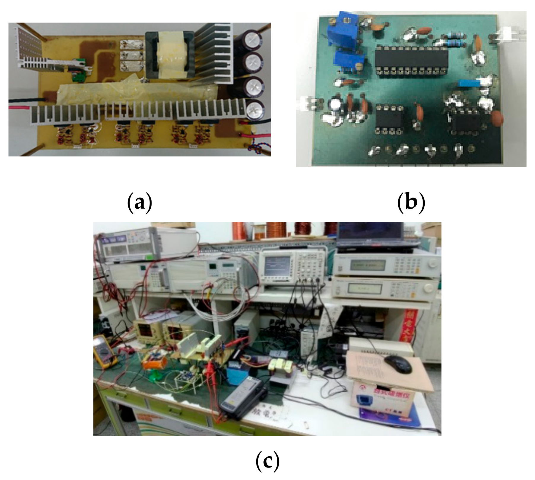
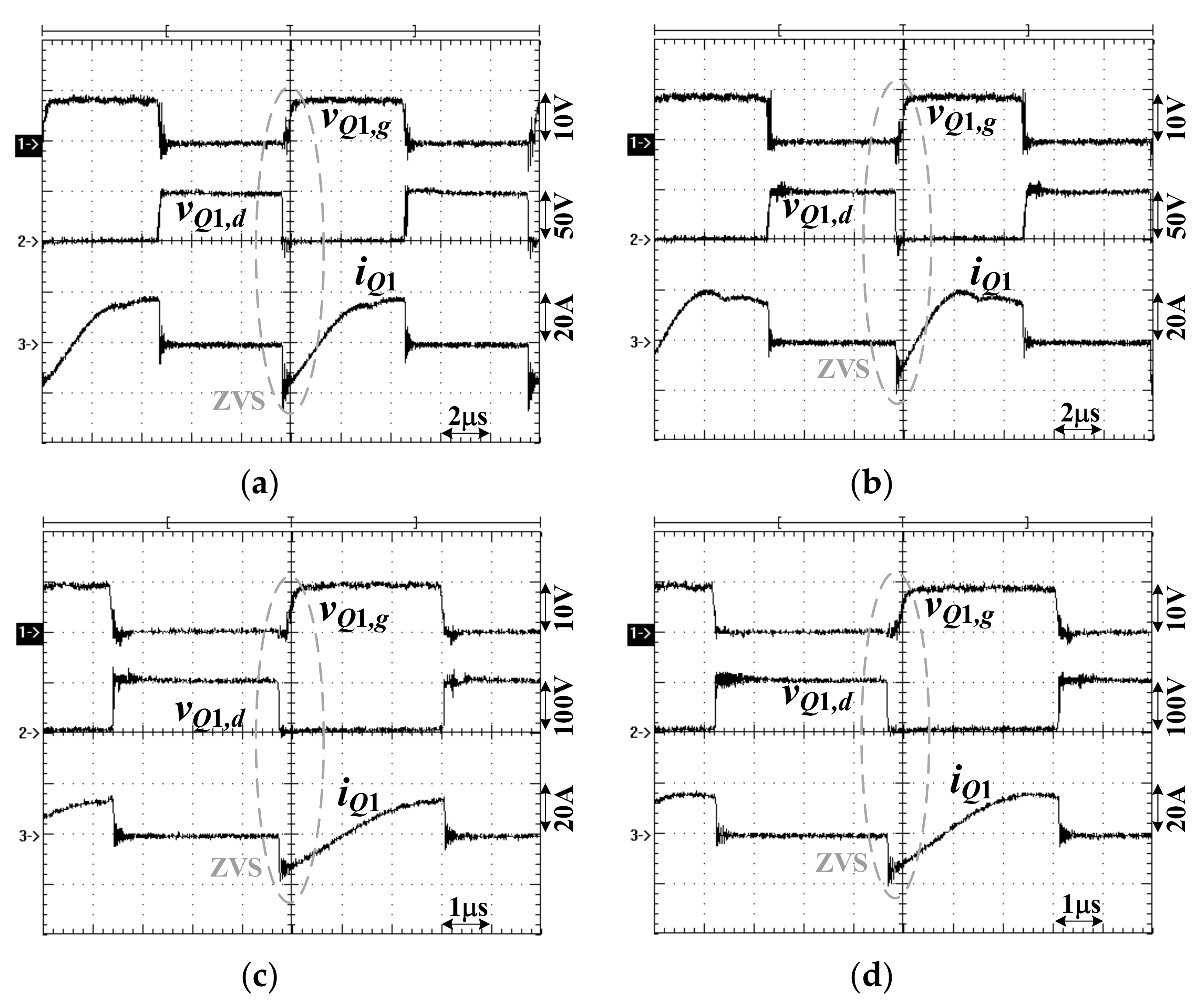
4. Design Procedures and Test Results

The design procedures and test results of the presented circuit are verified in this section. A laboratory circuit was built and the electric specifications were Vin = 50–400 V, Vo = 48 V, and Io,max = 10 A. The series resonant frequency was designed at 150 kHz. Due to Lr1 = Lr2 and Cr1 = Cr2, the series resonant frequencies for all three equivalent circuits shown in Figure 2 were identical and designed at 150 kHz. According to the voltage transfer function in Equation (5), the gain curves of the developed resonant converter with different input voltage ranges are given in Figure 7. The transition voltage Vin,tran 1 between the low and medium input voltage ranges was designed at 100 V with ±5 V voltage tolerance. Similarly, the transition voltage Vin,tran 2 between the medium and high input voltage ranges was designed at 200 V with ±5 V voltage tolerance. From Equation (6), one can observe that the voltage gain at the high input voltage range was about two (four) times of the voltage gain at the medium (low) input voltage range. The design procedures for three equivalent resonant circuits were almost identical. Therefore, the prototype circuit was designed at the low input voltage range to simplify the design consideration. The minimum voltage gain Gac,min at the series resonant frequency was designed as unity and the transition voltage Vin,trans 1 = 100 V. The turns ratio n1 = np/ns can be calculated from Equation (5) and expressed in Equation (7):
n 1 = G a c , m i n × V i n , t r a n   1 / V o = 1 × 100 / 48 2.08 .
Transformer T is implemented by the TDK (Tokyo Electric Chemical Industry Co., Ltd., Tokyo, Japan) magnetic core with ΔB = 0.4 tesla and Ae = 354 mm2. The series resonant frequency was selected at 150 kHz. The primary turns of transformer are obtained in Equation (8):
n p , m i n > n 1 V o / [ f s w Δ B A e = 2.08 × 48 / 150000 × 0.4 × 0.000354 ] 4.7 .
The actual primary turns and secondary turns in the prototype circuit were np = 8 and ns = 4. The equivalent resistance Req at the rated power is given in Equation (9):
R e q = 8 n 1 2 R o / π 2 = 8 × 2 2 × 48 / 10 / 3.14159 2 = 15.56   Ω .
The inductor ratio ln = Lm1/Lr1 = 3 and quality factor x = 0.25 were selected in the prototype circuit. Lr1 and Lr2 are obtained from Equation (10) and Cr1 and Cr2 are calculated in Equation (11):
L r 1 = L r 2 = x R e q 2 π f r = 4.13   μ H ,
C r 1 = C r 2 = 1 4 π 2 L r 1 f r 2 273   nF .
The magnetizing inductors Lm1 and Lm2 are expressed in Equation (12):
L m 1 = L m 2 = l n × L r 1 12.4   μ H .
The voltage stress of power MOSFETs (metal–oxide–semiconductor field-effect transistor) Q1Q6 and switch S was the maximum input voltage Vin,max = 400 V. The theoretical voltage ratings of the rectifier diodes D1 and D2 were 2Vo = 98 V. Figure 8 shows the control block of the signals Q1Q6 and S. Two Schmitt trigger comparators were used for transition voltages 100 and 200 V to select the correct range of input voltage. Figure 9 and Table 1 give the photographs and all circuit components used in the prototype circuit, respectively. Figure 9a shows the photograph of the prototype circuit. The control board for selecting the correct range of input voltage and the consequent bridge configuration is given in Figure 9b. The experimental setup, including the test equipment, is provided in Figure 9c. The list of equipment that was used to record the results is as follows: Chroma 62012P-600-8 (DC voltage source), Chroma 63112A (DC electronic load), TCP302 and TCP312 (current probe), TDS3014 (digital oscilloscope), and SI-9110 (isolated voltage probe).
The experimental waveforms of the developed circuit operated at low input voltage range (Vin = 50–100 V) are shown in Figure 10 and Figure 11. In the low input voltage range, power switches S, Q5, and Q6 were off and only switches Q1Q4 were controlled with frequency modulation. Figure 10 illustrates the experimental results at Vin = 50 V input and full load. Figure 10a gives the test waveforms of vQ1,gvQ4,g. The switching frequency fsw under the rated power and Vin = 50 V was about 100 kHz. Figure 10b provides the test waveforms of primary-side current iLr1, capacitor voltage vCr1, and leg voltage vab. Due to the switching frequency fsw = 100 kHz < fr = 150 kHz, the resonant current iLr1 was a quasi-resonant waveform. Figure 10c shows the experimental waveforms of Vo, Io, iD1, and iD2. One can observe that the output voltage was regulated at 48 V output, the load current Io was 10 A, and the diodes D1 and D2 turned off at zero current switching. Figure 11 gives the experimental results at the rated power and Vin = 95 V. The measured gate voltages vQ1,gvQ4,g are given in Figure 11a. The test results of vab, vCr1, and iLr1 are illustrated in Figure 11b. Because the switching frequency fsw at Vin = 95 V was almost equal to fr, the measured resonant inductor current iLr1 was a sinusoidal waveform. The experimental waveforms of Vo, Io, iD1, and iD2 at the rated power and Vin = 95 V are demonstrated in Figure 11c. Vo was regulated well at 48 V output under Io = 10 A. Figure 12 and Figure 13 give the test results under the medium input voltage range (Vin = 100–200 V). Under the medium input voltage range, switches Q3 and Q4 were off and S was on. Figure 12 shows the test results under Vin = 105 V and full load. Figure 12a gives the measured gate voltages vQ1,g, vQ2,g, vQ5,g, and vQ6,g. The measured switching frequency fsw was about 84 kHz. Figure 12b provides the test results of vCr1, iLr1, vCr2, and iLr2. Because fsw = 84 kHz < fr = 150 kHz, the resonant currents iLr1 and iLr2 were the quasi-sinusoidal waveforms. Figure 12c provides the measured waveforms of Vo, Io, iD1, and iD2 at the rated power and Vin = 105 V. The diodes D1 and D2 turned off at zero current switching. Similarly, the measured waveforms of the proposed converter under Vin = 195 V and full load are provided in Figure 13. The measured switching frequency fsw = 163 kHz at Vin = 195 V and full load so that iLr1 and iLr2 were the sinusoidal waveforms, as shown in Figure 13b. Under the high input voltage range (Vin = 200–400 V), power switches Q3, Q4, and Q5 were off, and S and Q6 were on. Figure 14 shows the experimental waveforms under Vin = 205 V, Vo = 48 V, and Po = 480 W. Figure 14a shows the measured gate voltages vQ1,g, vQ2,g, vS,g, and vQ6,g. The measured switching frequency fsw = 82 kHz at Vin = 205 V. Figure 14b provides the measured waveforms iLr1, iLr2, vCr1, and vCr2. Due to fsw (82 kHz) < fr (150 kHz), the measured currents iLr1 and iLr2 were the quasi-sinusoidal waveforms. Figure 14c gives the measured waveforms Vo, Io, iD1, and iD2. The diodes D1 and D2 turned off at zero current with soft switching operation. Figure 15 provides the experimental waveforms at the rated power and Vin = 400 V. The switching frequency fsw = 160 kHz. The measured switch waveforms of Q1 at Vin = 50, 95, 195, and 400 V cases are measured in Figure 16. One can observe that Q1 all turned on at zero voltage switching. It can be predicted that Q2Q6 were also turned on under zero voltage due to the LLC (inductor-inductor-capacitor) series resonant behavior. Figure 17 provides the measured circuit efficiencies for different load power (20%, 50%, and 100% loads) and input voltages (Vin = 50–400 V). For the same output power, the primary-side current at low input voltage range such as Vin = 50 V was greater than high input voltage range such as Vin = 205 V. This will introduce more conduction losses on the primary-side components under low input voltage range. Therefore, the presented circuit had better circuit efficiency at the high input voltage range.

5. Conclusions

The main contribution of the proposed converter is wide voltage operation capability compared to the conventional single-stage or two-stage converters. In conventional single-stage or two-stage PWM converters or resonant converters, the input voltage variation range is normally less than a 4:1 voltage range. The presented circuit has three equivalent operation circuits with half bridge to full bridge circuit topology to change the voltage gain between the output and input voltages. Each equivalent resonant circuit can achieve a 2:1 input voltage operation range, that is, Vin,max = 2Vin,min. Therefore, three equivalent resonant circuits can achieve an 8:1 wide input voltage range operation, that is, Vin,max = 8Vin,min. For the low input voltage range, the full-bridge resonant converter with low turns ratio of transformer is operated to obtain the higher voltage gain between the load voltage and input voltage. For the medium input voltage range, the other full bridge resonant circuit topology with high turns ratio is selected to obtain the lower voltage gain. The half bridge resonant converter is selected to achieve the lowest voltage gain under the high input voltage range. Therefore, the presented converter with three equivalent sub-circuits can accomplish an 8:1 wide input voltage operation. Due to resonant circuit characteristics, the power switches can have soft switching operation over wide range of load conditions. Three equivalent sub-circuits are selected according to the input voltage range with two Schmitt comparators. The applications of the presented resonant circuit can be the front stage of solar power conversion with wide input voltage variation. The theoretical converter characteristics were confirmed by the measured waveforms from a laboratory circuit. The measured results confirmed the converter performance with wide voltage range operation. The further works of this project are to increase the circuit efficiency by using the synchronous rectifiers on the output side and designing the isolated transformer with minimum core and copper losses.

Author Contributions

B.-R.L. proposed and designed this project and wrote this paper. Y.-S.Z. measured the circuit waveforms in the experiment. All authors have read and agreed to the published version of the manuscript.

Funding

This research is funded by the Ministry of Science and Technology, Taiwan, under grant number MOST 108-2221-E-224-022-MY2.

Acknowledgments

This research is funded by the Ministry of Science and Technology, Taiwan, under grant number MOST 108-2221-E-224-022-MY2.

Conflicts of Interest

The authors declare no potential conflict of interest.

References

  1. Liu, P.J.; Hsu, Y.C.; Hsu, S.R. Drain-voltage balance and phase-shifted PWM control schemes for high-efficiency parallel-string dimmable LED drivers. IEEE Trans. Ind. Electron. 2018, 65, 6168–6176. [Google Scholar] [CrossRef]
  2. Safaee, A.; Jain, P.; Bakhshai, A. A ZVS pulsewidth modulation full-bridge converter with a low-RMS-current resonant auxiliary circuit. IEEE Trans. Power Electron. 2016, 31, 4031–4047. [Google Scholar] [CrossRef]
  3. Wang, Y.; Zhang, S.; Guan, Y.; Liu, X.; Xu, D. Single-stage QR ac-dc converter based on buck-boost and flyback circuits. IET Power Electron. 2017, 10, 103–111. [Google Scholar] [CrossRef]
  4. Xie, X.; Li, J.; Peng, K.; Zhao, C.; Lu, Q. Study on the single-stage forward-flyback PFC converter with QR control. IEEE Trans. Power Electron. 2016, 31, 430–442. [Google Scholar] [CrossRef]
  5. Lin, B.R.; Chiang, H.K.; Chen, C.C. Analysis and implementation of a zvs-pwm converter with series-connected transformers. IEEE Trans. Circuits Syst. II 2007, 54, 917–921. [Google Scholar] [CrossRef]
  6. Lin, B.R.; Lin, Y. Parallel current-fed resonant converter with balance current sharing and no input ripple current. IET Power Electron. 2019, 12, 212–219. [Google Scholar] [CrossRef]
  7. Haga, H.; Kurokawa, F. Modulation method of a full-bridge three-level LLC resonant converter for battery charger of electric vehicles. IEEE Trans. Power Electron. 2017, 32, 2498–2507. [Google Scholar] [CrossRef]
  8. Zhang, Y.; Fu, C.; Sumner, M.; Wang, P. A wide input-voltage range quasi-Z-source boost DC–DC converter with high-voltage gain for fuel cell vehicles. IEEE Trans. Ind. Electron. 2018, 65, 5201–5212. [Google Scholar] [CrossRef] [Green Version]
  9. Yao, Z.; Xu, J. A three-phase DC-DC converter for low and wide input-voltage range application. In Proceedings of the 2016 IEEE Transportation Electrification Conference and Expo, Asia-Pacific (ITEC Asia-Pacific), Busan, Korea, 1–4 June 2016; pp. 208–213. [Google Scholar]
  10. Li, W.; Zong, S.; Liu, F.; Yang, H.; He, X.; Wu, B. Secondary-side phase-shift-controlled ZVS DC/DC converter with wide voltage gain for high input voltage applications. IEEE Trans. Power Electron. 2013, 28, 5128–5139. [Google Scholar] [CrossRef]
  11. Lu, J.; Kumar, A.; Afridi, K.K. Step-down impedance control network resonant DC-DC converter utilizing an enhanced phase-shift control for wide-input-range operation. IEEE Trans. Ind. Appl. 2018, 54, 4523–4536. [Google Scholar] [CrossRef]
  12. Wu, H.; Wan, C.; Sun, K.; Xing, Y. A high step-down multiple output converter with wide input voltage range based on quasi two-stage architecture and dual-output LLC resonant converter. IEEE Trans. Power Electron. 2015, 30, 1793–1796. [Google Scholar] [CrossRef]
  13. Hu, H.; Fang, X.; Chen, F.; Shen, Z.J.; Batarseh, I. A modified high-efficiency LLC converter with two transformers for wide input-voltage range applications. IEEE Trans. Power Electron. 2012, 28, 1946–1960. [Google Scholar] [CrossRef]
  14. Shang, C.; Liu, L.; Liu, M.; Men, S. A highly-efficient two-stage DC-DC converter with wide input voltage. In Proceedings of the 2015 IEEE International Telecommunications Energy Conference (INTELEC), Osaka, Japan, 18–22 October 2015; pp. 1–6. [Google Scholar]
  15. Zhou, G.; Ruan, X.; Wang, X. Input voltage feed-forward control strategy for cascaded DC/DC converters with wide input voltage range. In Proceedings of the 2016 IEEE 8th International Power Electronics and Motion Control Conference (IPEMC-ECCE Asia), Hefei, China, 22–26 May 2016; pp. 603–608. [Google Scholar]
  16. Jeong, Y.; Kim, J.K.; Lee, J.B.; Moon, G.W. An asymmetric half-bridge resonant converter having a reduced conduction loss for DC/DC power applications with a wide range of low input voltage. IEEE Trans. Power Electron. 2017, 32, 7795–7804. [Google Scholar] [CrossRef]
  17. Wang, P.; Zhou, L.; Zhang, Y.; Li, J.; Sumner, M. Input-parallel output-series DC-DC boost converter with a wide input voltage range, for fuel cell vehicles. IEEE Trans. Veh. Technol. 2017, 66, 7771–7781. [Google Scholar] [CrossRef]
  18. Kim, B.; Kim, S.; Huh, D.Y.; Choi, J.H.; Kim, M. Hybrid resonant half-bridge DC/DC converter with wide input voltage range. In Proceedings of the 2018 IEEE Applied Power Electronics Conference and Exposition (APEC), San Antonio, TX, USA, 4–8 March 2018; pp. 1876–1881. [Google Scholar]
  19. Singh, A.K.; Das, P.; Panda, S.K. Analysis and design of SQR-based high-voltage LLC resonant dc-dc converter. IEEE Trans. Power Electron. 2017, 32, 4466–4481. [Google Scholar] [CrossRef]
  20. Sun, W.; Xing, Y.; Wu, H.; Ding, J. Modified high-efficiency LLC converters with two split resonant branches for wide input-voltage range applications. IEEE Trans. Power Electron. 2018, 33, 7867–7870. [Google Scholar] [CrossRef]
  21. Jovanović, M.M.; Irving, B.T. On the fly topology-morphing control efficiency optimization method for LLC resonant converters operating in wide input and/or output-voltage range. IEEE Trans. Power Electron. 2016, 31, 2596–2608. [Google Scholar] [CrossRef]
  22. Steigerwald, R.L. A comparison of half-bridge resonant converter topologies. IEEE Trans. Power Electron. 1988, 3, 174–182. [Google Scholar] [CrossRef]
Figure 1. Circuit schematic of the developed converter.
Applsci 10 00310 g001
Figure 2. Circuit diagrams for different input voltage ranges: (a) low input voltage (Vin,L = Vin,max/8–Vin,max/4); (b) medium input voltage (Vin,M = Vin,max/4–Vin,max/2); (c) high input voltage (Vin,H = Vin,max/2–Vin,max).
Applsci 10 00310 g002
Figure 3. Proposed direct current (DC) converter under low input voltage range: (a) pulse-width modulation (PWM) waveforms; (b) state 1; (c) state 2; (d) state 3; (e) state 4; (f) state 5; (g) state 6.
Applsci 10 00310 g003aApplsci 10 00310 g003b
Figure 4. Proposed DC converter under medium input voltage range: (a) PWM waveforms; (b) state 1; (c) state 2; (d) state 3; (e) state 4; (f) state 5; (g) state 6.
Applsci 10 00310 g004aApplsci 10 00310 g004b
Figure 5. Proposed DC converter under high input voltage range: (a) PWM waveforms; (b) state 1; (c) state 2; (d) state 3; (e) state 4; (f) state 5; (g) state 6.
Applsci 10 00310 g005aApplsci 10 00310 g005b
Figure 6. Equivalent circuit of the resonant tank.
Applsci 10 00310 g006
Figure 7. Voltage curves of the presented circuit: (a) low input voltage range; (b) medium input voltage range; (c) high input voltage range.
Applsci 10 00310 g007aApplsci 10 00310 g007b
Figure 8. Control block of the signals Q1Q6 and S.
Applsci 10 00310 g008
Figure 9. Pictures of the proposed converter: (a) prototype circuit; (b) control board; (c) experimental setup.
Applsci 10 00310 g009
Figure 10. Experimental results at Vin = 50 V and full load: (a) vQ1,g~vQ4,g; (b) vab, vCr1, iLr1; (c) Vo, Io, iD1, iD2.
Applsci 10 00310 g010
Figure 11. Experimental results at Vin = 95 V and full load: (a) vQ1,g~vQ4,g; (b) vab, vCr1, iLr1; (c) Vo, Io, iD1, iD2.
Applsci 10 00310 g011
Figure 12. Experimental results at Vin = 105 V and full load: (a) vQ1,g, vQ2,g, vQ5,g, vQ6,g; (b) vCr1, iLr1, vCr2, iLr2; (c) Vo, Io, iD1, iD2.
Applsci 10 00310 g012
Figure 13. Experimental results at Vin = 195 V and full load: (a) vQ1,g, vQ2,g, vQ5,g, vQ6,g; (b) vCr1, iLr1, vCr2, iLr2; (c) Vo, Io, iD1, iD2.
Applsci 10 00310 g013
Figure 14. Experimental results at Vin = 205 V and full load: (a) vQ1,g, vQ2,g, vS,g, vQ6,g; (b) vCr1, iLr1, vCr2, iLr2; (c) Vo, Io, iD1, iD2.
Applsci 10 00310 g014
Figure 15. Experimental results at Vin = 400 V and full load: (a) vQ1,g, vQ2,g, vS,g, vQ6,g; (b) vCr1, iLr1, vCr2, iLr2; (c) Vo, Io, iD1, iD2.
Applsci 10 00310 g015
Figure 16. Experimental results at switch Q1 under (a) Vin = 50 V and 50% load; (b) Vin = 50 V and 100% load; (c) Vin = 95 V and 50% load; (d) Vin = 95 V and 100% load; (e) Vin = 195 V and 50% load; (f) Vin = 195 V and 100% load; (g) Vin = 400 V and 50% load; (h) Vin = 400 V and 100% load.
Applsci 10 00310 g016aApplsci 10 00310 g016b
Figure 17. Measured circuit efficiencies: (a) low input voltage range; (b) medium input voltage; (c) high input voltage range.
Applsci 10 00310 g017aApplsci 10 00310 g017b
Table 1. Prototype circuit parameters.
ItemsSymbolParameter
Input voltageVin50–400 V
Output voltageVo48 V
Rated load currentIo10 A
Series resonant frequencyfr150 kHz
Output capacitorCo1080 μF (1080 μF/100 V)
Resonant capacitorsCr1, Cr2273 nF
Power MOSFETsQ1Q6, SInfineon-6R070P6
Resonant inductorsLr1, Lr24.13 μH
Rectifier diodesD1, D2PS30M100SFP
Primary and secondary turns of Tnp, ns8 turns, 4 turns

