An Approach to the Extreme Miniaturization of Rotary Comb Drives

 ,
,  ,
,  ,
,  , , ,
, , ,  and
and 
Abstract
1. Introduction
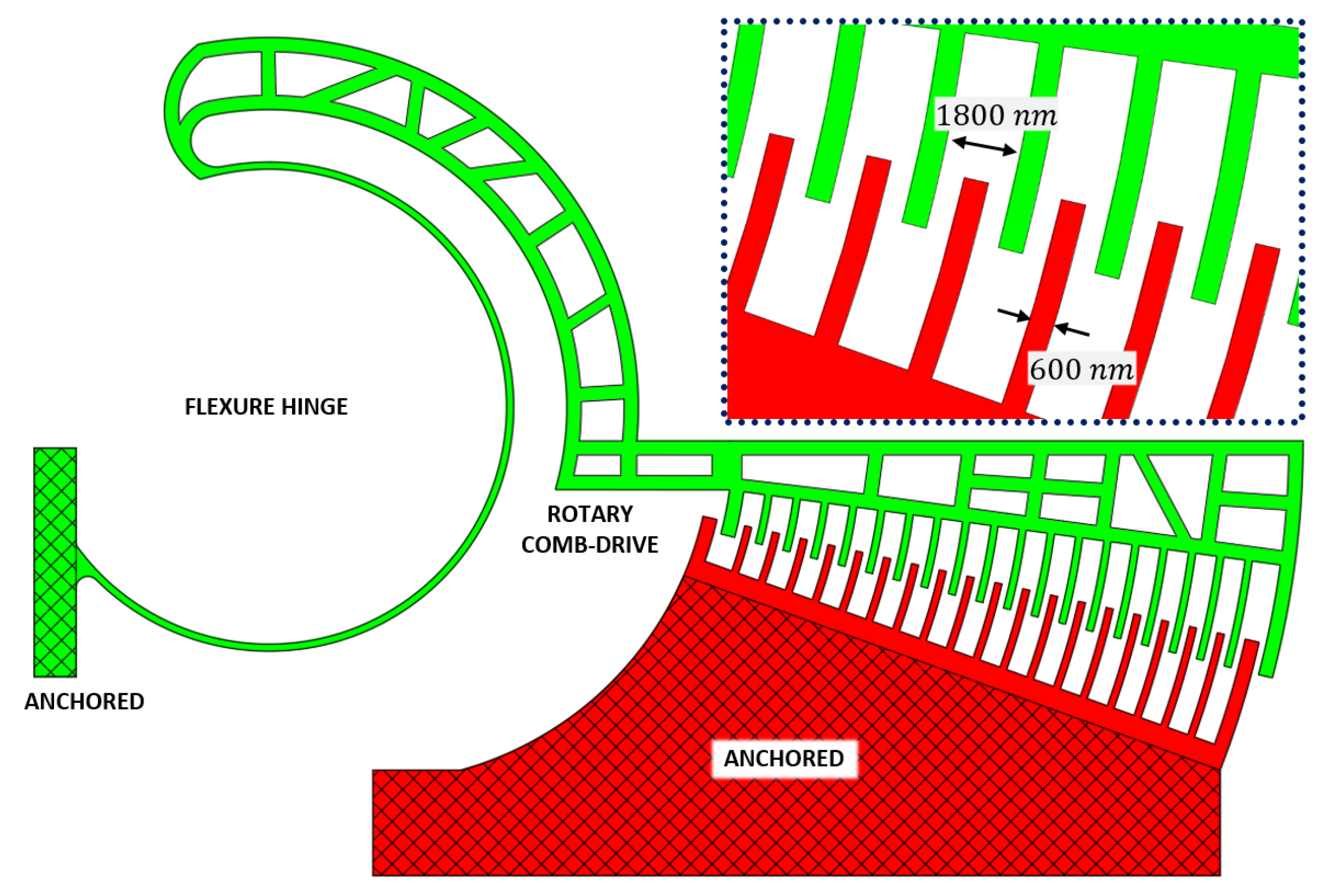
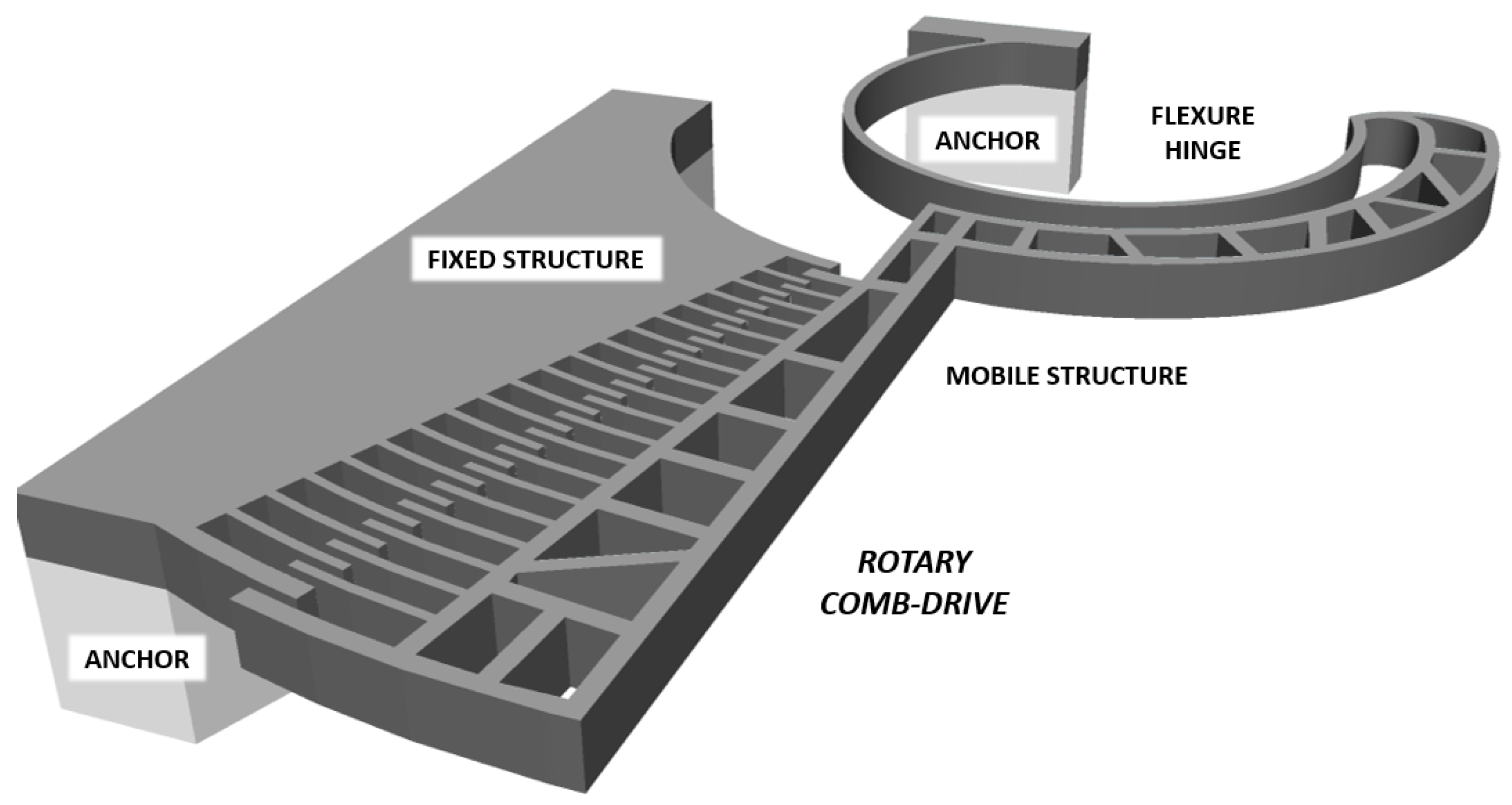
2. A Nano-Scaled Rotary Comb-Drive Electrostatic Actuator
- A fixed part (red colored), with interdigitated fingers;
- A suspended part (green colored), composed by a mobile rigid body with interdigitated fingers and a flexure hinge with an anchored part on the left.
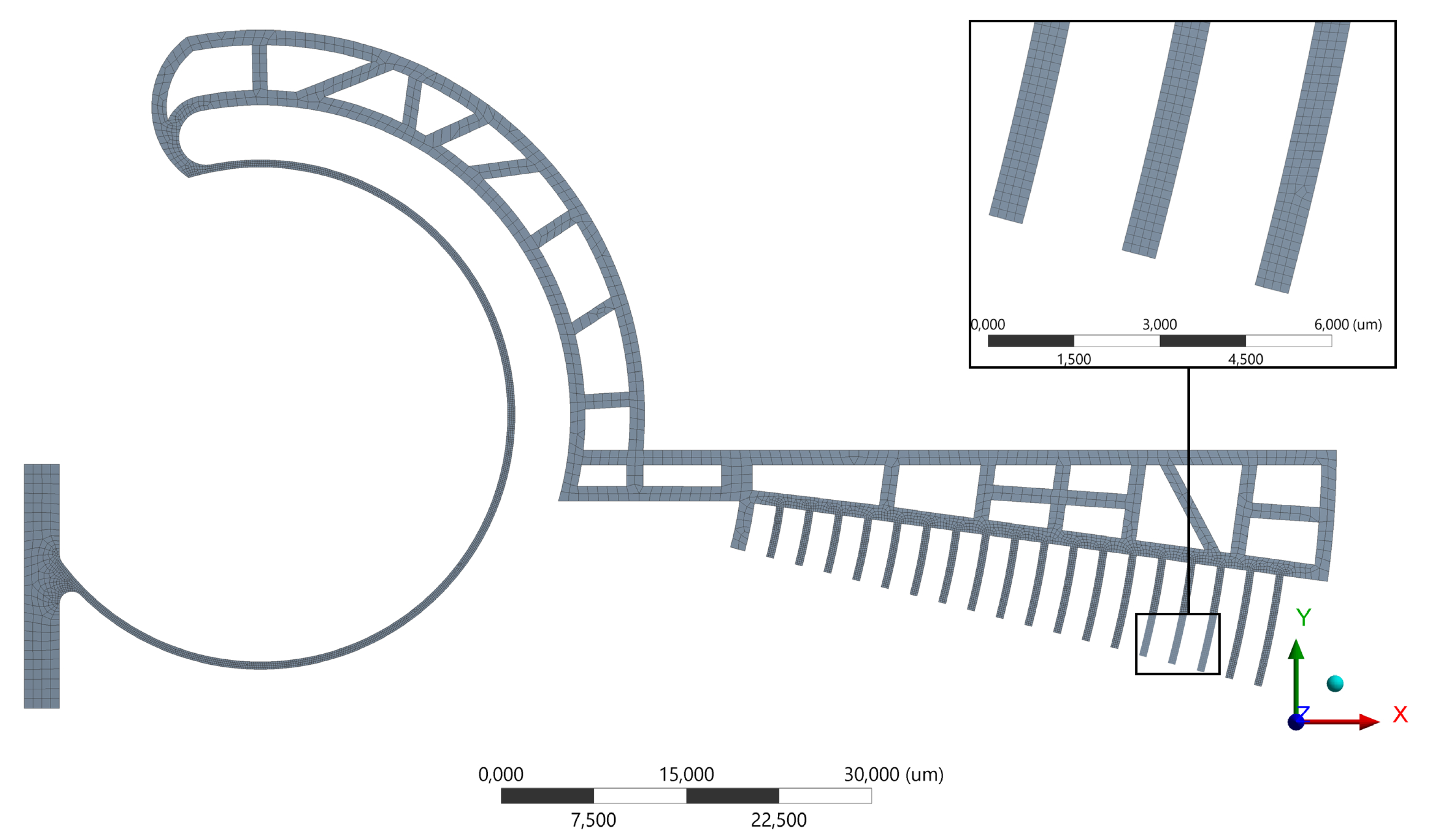
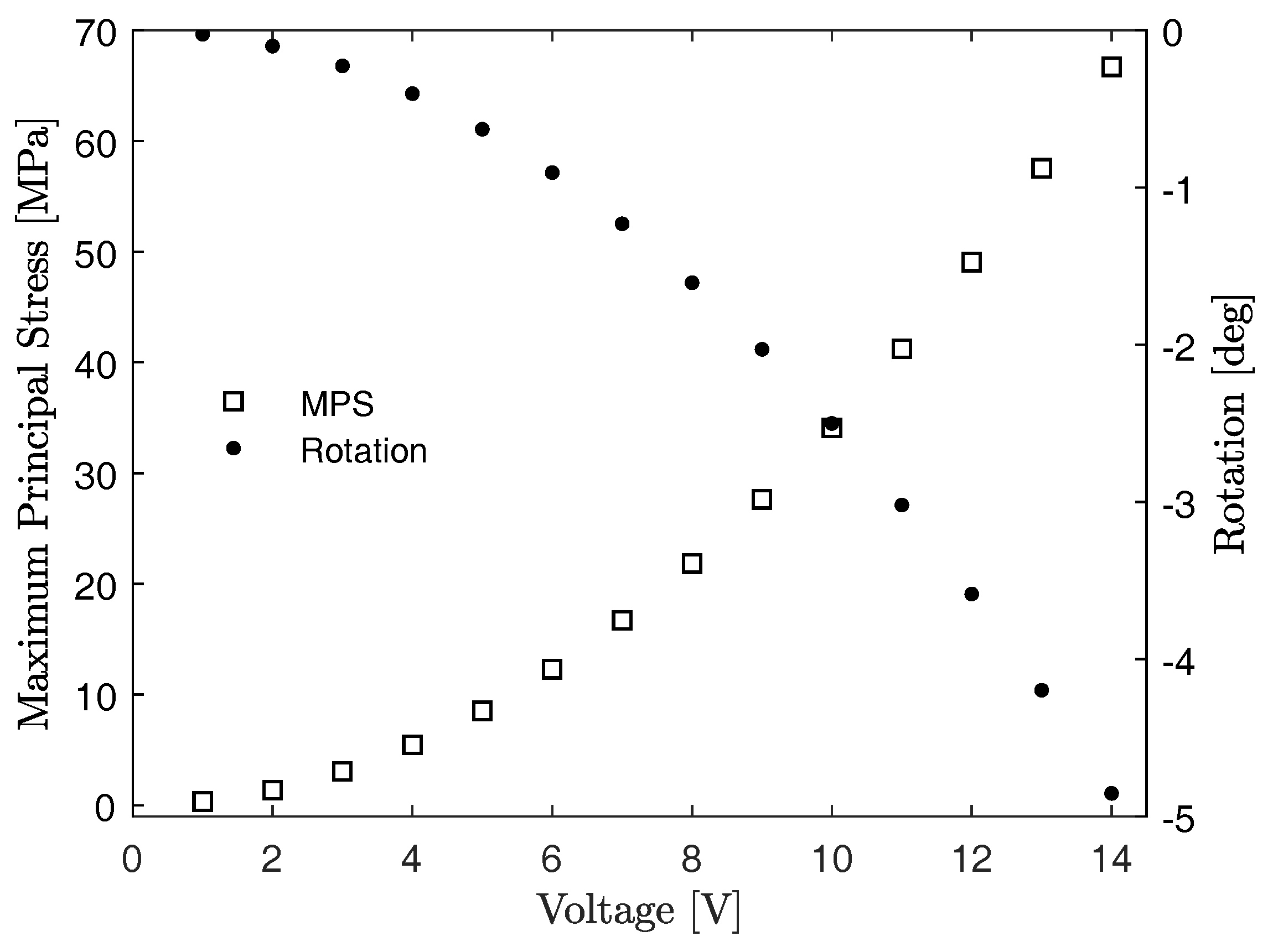
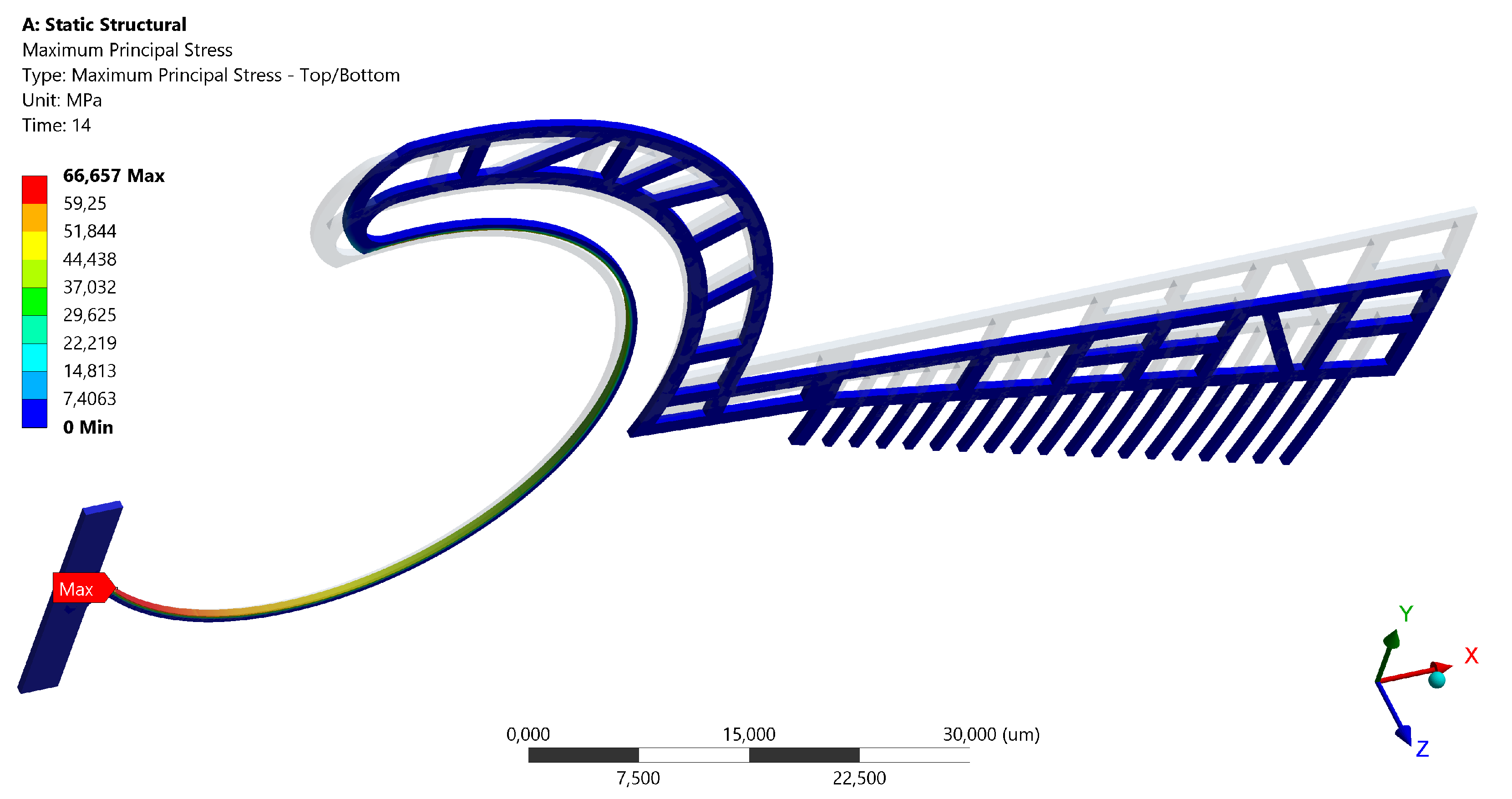
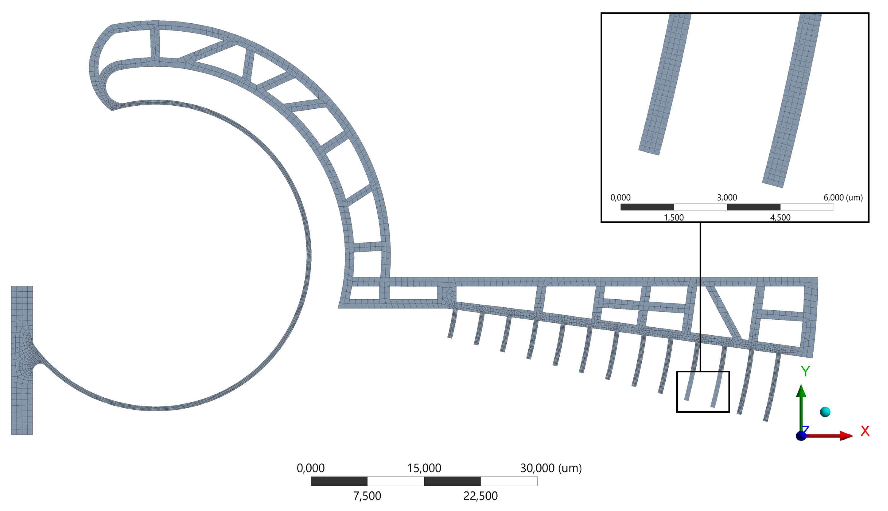
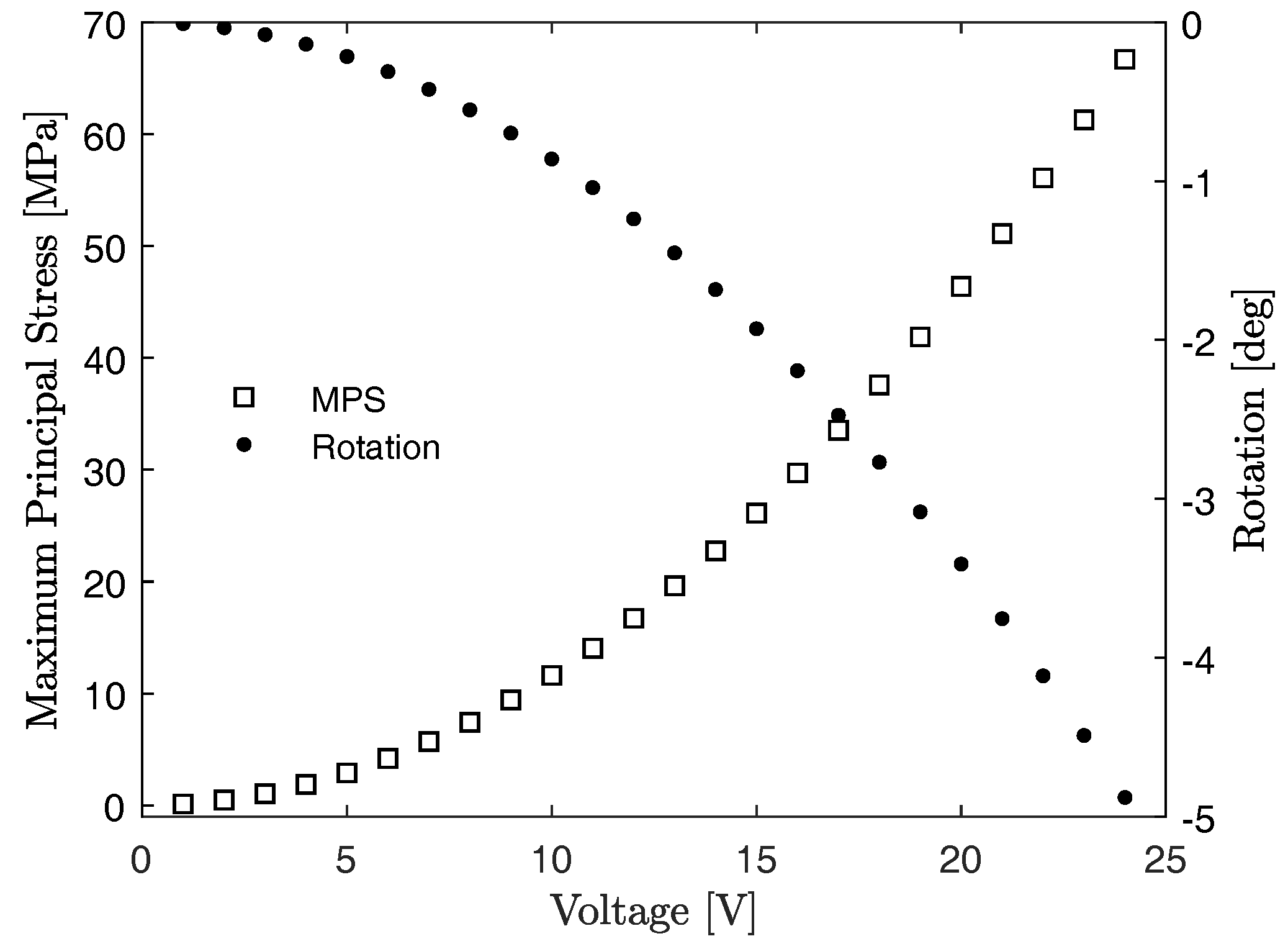
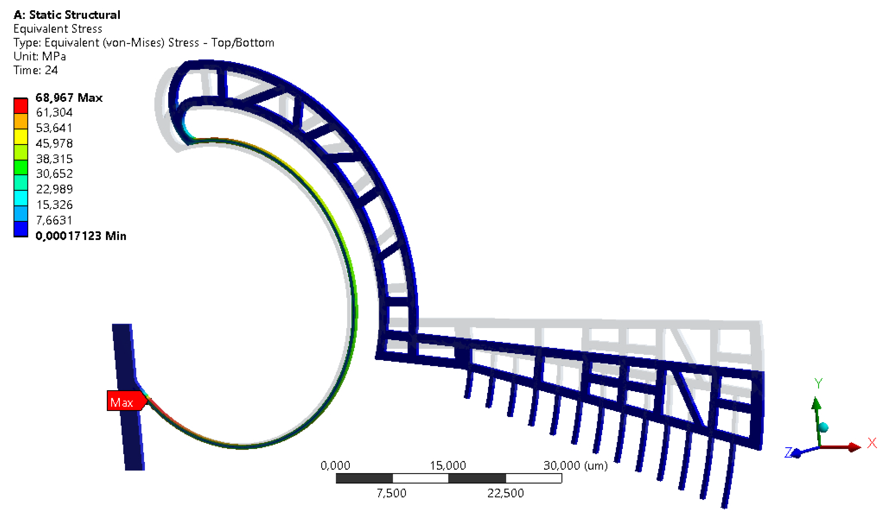
3. Microelectromechanical Simulation
3.1. First Layout
3.2. Second Layout
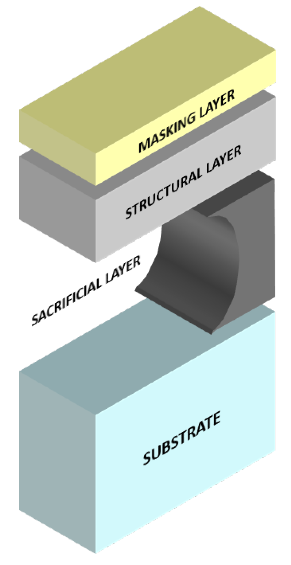
4. Fabrication
- Deposition/growth of a chosen material on a substrate in form of thin/thick film, using various kinds of methods, such as Physical or Chemical Vapor Deposition (PVD/CVD), Atomic Layer Deposition (ALD) and Epitaxy;
- Geometry definition of the latter, usually via lithographic techniques or similar;
- Material patterning, via wet/dry etching procedures.
- A glass substrate;
- A Ti/W metallic alloy as intermediate sacrificial layer;
- Doped hydrogenated amorphous silicon (a-Si:H) as structural layer: a highly versatile material, suitable for large-area and low-cost electronic devices, biologically compatible, while monolithically integrable on rigid or flexible, metallic, dielectric or polymeric substrates [37,38,39,40,41,42]. It also shows interesting mechanical features and was chosen to build bridge-like structures and cantilevers based devices [43].
- Chromium as masking layer for the structure patterning.
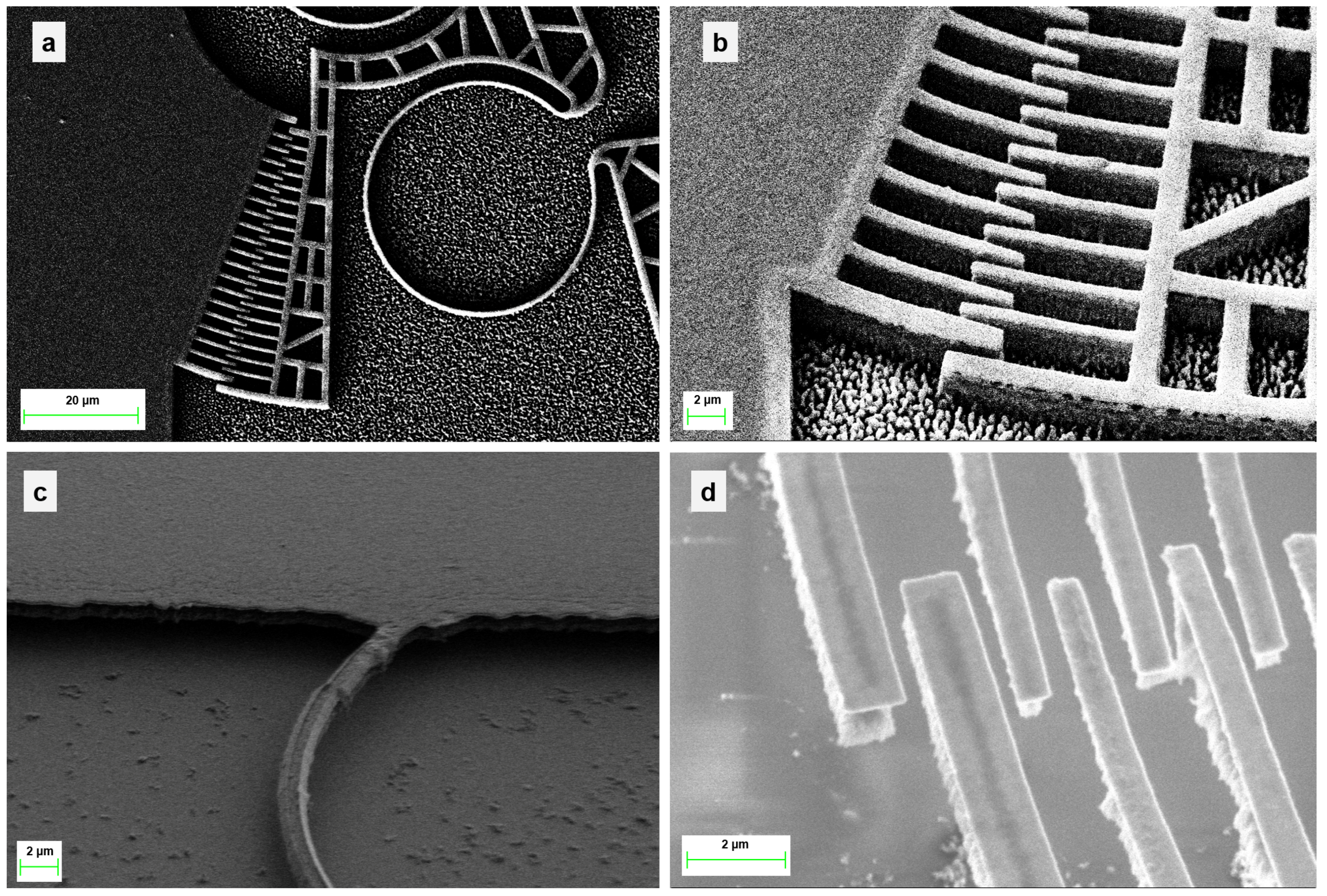
- PVD of the sacrificial layer;
- CVD of the amorphous silicon layer;
- Geometry definition on a PVD obtained chromium film by lithographic technique: in particular, Electron Beam Lithography (EBL) was required, in order to obtain submicrometric resolution, on an electron-sensible polymeric film [44];
- Structure patterning by Reactive Ion Etching (RIE) technique, with the previously shaped chromium film as masking layer;
- Structure releasing via isotropic and selective removal of the intermediate layer, in a wet etching solution. Etch holes in the rigid suspended bodies were considered in order to promote the under-etching phenomenon and optimize the releasing process.
- A substrate temperature of 200 °C;
- A SiH4 flow of 45 sccm and a PH3 flow of 10 sccm into the process chamber, with a process pressure of 0.3 Torr;
- A glow discharge with a power density of 25 mW/cm2, for 1 h.
5. Conclusions
Author Contributions
Conflicts of Interest
References
- Gardner, J.W.; Varadan, V.K.; Awadelkarim, O.O. Microsensors. In Microsensors, MEMS, and Smart Devices; John Wiley & Sons, Ltd.: Hoboken, NJ, USA, 2001; pp. 227–302. [Google Scholar]
- Bhushan, B. Nanotribology and nanomechanics of MEMS/NEMS and BioMEMS/BioNEMS materials and devices. In Nanotribology and Nanomechanics; Springer: Cham, Switzerland, 2017; pp. 797–907. [Google Scholar]
- Grayson, A.C.R.; Shawgo, R.S.; Johnson, A.M.; Flynn, N.T.; Li, Y.; Cima, M.J.; Langer, R. A BioMEMS review: MEMS technology for physiologically integrated devices. Proc. IEEE 2004, 92, 6–21. [Google Scholar] [CrossRef]
- Tilmans, H.A.; De Raedt, W.; Beyne, E. MEMS for wireless communications: From RF-MEMS components to RF-MEMS-SiP. J. Micromech. Microeng. 2003, 13, S139. [Google Scholar] [CrossRef]
- Saxena, V.; Plum, T.J.; Jessing, J.R.; Baker, R.J. Design and fabrication of a MEMS capacitive chemical sensor system. In Proceedings of the 2006 IEEE Workshop on Microelectronics and Electron Devices, WMED’06, Boise, ID, USA, 14 April 2006. [Google Scholar]
- Bell, D.J.; Lu, T.; Fleck, N.A.; Spearing, S.M. MEMS actuators and sensors: Observations on their performance and selection for purpose. J. Micromech. Microeng. 2005, 15, S153. [Google Scholar] [CrossRef]
- Del Corro, P.G.; Imboden, M.; Pérez, D.J.; Bishop, D.J.; Pastoriza, H. Single ended capacitive self-sensing system for comb drives driven XY nanopositioners. Sens. Actuators A Phys. 2018, 271, 409–417. [Google Scholar] [CrossRef]
- Thielicke, E.; Obermeier, E. Microactuators and their technologies. Mechatronics 2000, 10, 431–455. [Google Scholar] [CrossRef]
- Legtenberg, R.; Groeneveld, A.; Elwenspoek, M. Comb-drive actuators for large displacements. J. Micromech. Microeng. 1996, 6, 320. [Google Scholar] [CrossRef]
- Xie, H.; Pan, Y.; Fedder, G.K. A CMOS-MEMS mirror with curled-hinge comb drives. J. Microelectromech. Syst. 2003, 12, 450–457. [Google Scholar]
- Yi, B.J.; Chung, G.B.; Na, H.Y.; Kim, W.K.; Suh, I.H. Design and experiment of a 3-DOF parallel micromechanism utilizing flexure hinges. IEEE Trans. Robot. Autom. 2003, 19, 604–612. [Google Scholar]
- Belfiore, N.P.; Scaccia, M.; Ianniello, F.; Presta, M. Selective Compliance Hinge. U.S. Patent 8,191,204 B2, 6 May 2012. [Google Scholar]
- Balucani, M.; Belfiore, N.P.; Crescenzi, R.; Genua, M.; Verotti, M. Developing and modeling a plane 3 DOF compliant micromanipulator by means of a dedicated MBS code. In Proceedings of the 2011 NSTI Nanotechnology Conference and Expo, Boston, MA, USA, 13–16 June 2011; Volume 2, pp. 659–662. [Google Scholar]
- Balucani, M.; Belfiore, N.P.; Crescenzi, R.; Verotti, M. The development of a MEMS/NEMS-based 3 D.O.F. compliant micro robot. Int. J. Mech. Control 2011, 12, 3–10. [Google Scholar]
- Belfiore, N.P.; Balucani, M.; Crescenzi, R.; Verotti, M. Performance analysis of compliant mems parallel robots through pseudo-rigid-body model synthesis. In Proceedings of the ASME 2012 11th Biennial Conference on Engineering Systems Design and Analysis, Nantes, France, 2–4 July 2012; Volume 3, pp. 329–334. [Google Scholar]
- Belfiore, N.P.; Emamimeibodi, M.; Verotti, M.; Crescenzi, R.; Balucani, M.; Nenzi, P. Kinetostatic optimization of a MEMS-based compliant 3 DOF plane parallel platform. In Proceedings of the ICCC 2013–IEEE 9th International Conference on Computational Cybernetics, Tihany, Hungary, 8–10 July 2013; pp. 261–266. [Google Scholar]
- Sanò, P.; Verotti, M.; Bosetti, P.; Belfiore, N.P. Kinematic Synthesis of a D-Drive MEMS Device with Rigid-Body Replacement Method. J. Mech. Des. Trans. ASME 2018, 140, 075001. [Google Scholar] [CrossRef]
- Verotti, M.; Crescenzi, R.; Balucani, M.; Belfiore, N.P. MEMS-based conjugate surfaces flexure hinge. J. Mech. Des. Trans. ASME 2015, 137, 012301. [Google Scholar] [CrossRef]
- Belfiore, N.P.; Broggiato, G.; Verotti, M.; Balucani, M.; Crescenzi, R.; Bagolini, A.; Bellutti, P.; Boscardin, M. Simulation and construction of a MEMS CSFH based microgripper. Int. J. Mech. Control 2015, 16, 21–30. [Google Scholar]
- Belfiore, N.P.; Broggiato, G.; Verotti, M.; Crescenzi, R.; Balucani, M.; Bagolini, A.; Bellutti, P.; Boscardin, M. Development of a MEMS technology CSFH based microgripper. In Proceedings of the 23rd International Conference on Robotics in Alpe-Adria-Danube Region (RAAD), Smolenice, Slovakia, 3–5 September 2014. [Google Scholar]
- Crescenzi, R.; Balucani, M.; Belfiore, N.P. Operational characterization of CSFH MEMS technology based hinges. J. Micromech. Microeng. 2018, 28. [Google Scholar] [CrossRef]
- Di Giamberardino, P.; Bagolini, A.; Bellutti, P.; Rudas, I.; Verotti, M.; Botta, F.; Belfiore, N. New MEMS tweezers for the viscoelastic characterization of soft materials at the microscale. Micromachines 2017, 9, 15. [Google Scholar] [CrossRef]
- Bagolini, A.; Ronchin, S.; Bellutti, P.; Chistè, M.; Verotti, M.; Belfiore, N.P. Fabrication of Novel MEMS Microgrippers by Deep Reactive Ion Etching With Metal Hard Mask. J. Microelectromech. Syst. 2017, 26, 926–934. [Google Scholar] [CrossRef]
- Dochshanov, A.; Verotti, M.; Belfiore, N. A Comprehensive Survey on Microgrippers Design: Operational Strategy. J. Mech. Des. Trans. ASME 2017, 139, 070801. [Google Scholar] [CrossRef]
- Verotti, M.; Dochshanov, A.; Belfiore, N.P. A Comprehensive Survey on Microgrippers Design: Mechanical Structure. J. Mech. Des. Trans. ASME 2017, 139, 060801. [Google Scholar] [CrossRef]
- Verotti, M.; Dochshanov, A.; Belfiore, N.P. Compliance Synthesis of CSFH MEMS-Based Microgrippers. J. Mech. Des. Trans. ASME 2017, 139. [Google Scholar] [CrossRef]
- Potrich, C.; Lunelli, L.; Bagolini, A.; Bellutti, P.; Pederzolli, C.; Verotti, M.; Belfiore, N.P. Innovative silicon microgrippers for biomedical applications: Design, mechanical simulation and evaluation of protein fouling. Actuators 2018, 7, 12. [Google Scholar] [CrossRef]
- Veroli, A.; Buzzin, A.; Crescenzi, R.; Frezza, F.; de Cesare, G.; D’Andrea, V.; Mura, F.; Verotti, M.; Dochshanov, A.; Belfiore, N.P. Development of a NEMS-Technology Based Nano Gripper. In Proceedings of the International Conference on Robotics in Alpe-Adria Danube Region, Torino, Italy, 21–23 June 2017; Springer: Cham, Switzerland, 2017; pp. 601–611. [Google Scholar]
- Buzzin, A.; Veroli, A.; de Cesare, G.; Belfiore, N. Nems-Technology based nano gripper for mechanic manipulation in space exploration mission. Adv. Astronaut. Sci. 2018, 163, 61–67. [Google Scholar]
- Nascetti, A.; Caputo, D.; Scipinotti, R.; de Cesare, G. Technologies for autonomous integrated lab-on-chip systems for space missions. Acta Astronaut. 2016, 128, 401–408. [Google Scholar] [CrossRef]
- Hou, M.T.K.; Huang, J.Y.; Jiang, S.S.; Yeh, J.A. In-plane rotary comb-drive actuator for a variable optical attenuator. J. Micro/Nanolithogr. MEMS MOEMS 2008, 7, 043015. [Google Scholar]
- Cho, S.; Chasiotis, I. Elastic properties and representative volume element of polycrystalline silicon for MEMS. Exp. Mech. 2007, 47, 37–49. [Google Scholar] [CrossRef]
- Sharpe, W.N.; Yuan, B.; Vaidyanathan, R.; Edwards, R.L. Measurements of Young’s modulus, Poisson’s ratio, and tensile strength of polysilicon. In Proceedings of the IEEE The Tenth Annual International Workshop on Micro Electro Mechanical Systems. An Investigation of Micro Structures, Sensors, Actuators, Machines and Robots, Nagoya, Japan, 26–30 January 1997; pp. 424–429. [Google Scholar]
- Sharpe, W.N., Jr.; Yuan, B.; Vaidyanathan, R.; Edwards, R.L. New test structures and techniques for measurement of mechanical properties of MEMS materials. In Proceedings of the Micromachining and Microfabrication, Austin, TX, USA, 13 September 1996; Volume 2880, pp. 78–91. [Google Scholar]
- Volland, B.; Heerlein, H.; Rangelow, I. Electrostatically driven microgripper. Microelectr. Eng. 2002, 61, 1015–1023. [Google Scholar] [CrossRef]
- Caputo, D.; Ceccarelli, M.; de Cesare, G.; Nascetti, A.; Scipinotti, R. Lab-on-glass system for DNA analysis using thin and thick film technologies. MRS Online Proc. Libr. Arch. 2009, 1191, 53–58. [Google Scholar] [CrossRef]
- De Cesare, G.; Gavesi, M.; Palma, F.; Riccò, B. A novel a-Si: H mechanical stress sensor. Thin Solid Films 2003, 427, 191–195. [Google Scholar] [CrossRef]
- Caputo, D.; de Cesare, G.; Nardini, M.; Nascetti, A.; Scipinotti, R. Monitoring of temperature distribution in a thin film heater by an array of a-Si: H temperature sensors. IEEE Sens. J. 2012, 12, 1209–1213. [Google Scholar] [CrossRef]
- De Cesare, G.; Nascetti, A.; Caputo, D. Amorphous silicon pin structure acting as light and temperature sensor. Sensors 2015, 15, 12260–12272. [Google Scholar] [CrossRef] [PubMed]
- Tucci, M.; Serenelli, L.; Salza, E.; De Iuliis, S.; Geerligs, L.; Caputo, D.; Ceccarelli, M.; de Cesare, G. Back contacted a-Si: H/c-Si heterostructure solar cells. J. Non-Cryst. Solids 2008, 354, 2386–2391. [Google Scholar] [CrossRef]
- Caputo, D.; de Cesare, G. New a-Si: H two-terminal switching device for active display. J. Non-Cryst. Solids 1996, 198, 1134–1136. [Google Scholar] [CrossRef]
- Asquini, R.; Buzzin, A.; Caputo, D.; de Cesare, G. Integrated Evanescent Waveguide Detector for Optical Sensing. IEEE Trans. Compon. Packag. Manuf. Technol. 2018, 8, 1180–1186. [Google Scholar] [CrossRef]
- Gaspar, J.; Chu, V.; Conde, J. Amorphous silicon electrostatic microresonators with high quality factors. Appl. Phys. Lett. 2004, 84, 622–624. [Google Scholar] [CrossRef]
- Veroli, A.; Mura, F.; Balucani, M.; Caminiti, R. Dose influence on the PMMA e-resist for the development of high-aspect ratio and reproducible sub-micrometric structures by electron beam lithography. AIP Conf. Proc. 2016, 1749, 020010. [Google Scholar]


© 2018 by the authors. Licensee MDPI, Basel, Switzerland. This article is an open access article distributed under the terms and conditions of the Creative Commons Attribution (CC BY) license (http://creativecommons.org/licenses/by/4.0/).
Share and Cite
Veroli, A.; Buzzin, A.; Frezza, F.; De Cesare, G.; Hamidullah, M.; Giovine, E.; Verotti, M.; Belfiore, N.P. An Approach to the Extreme Miniaturization of Rotary Comb Drives. Actuators 2018, 7, 70. https://doi.org/10.3390/act7040070
Veroli A, Buzzin A, Frezza F, De Cesare G, Hamidullah M, Giovine E, Verotti M, Belfiore NP. An Approach to the Extreme Miniaturization of Rotary Comb Drives. Actuators. 2018; 7(4):70. https://doi.org/10.3390/act7040070
Chicago/Turabian StyleVeroli, Andrea, Alessio Buzzin, Fabrizio Frezza, Giampiero De Cesare, Muhammad Hamidullah, Ennio Giovine, Matteo Verotti, and Nicola Pio Belfiore. 2018. "An Approach to the Extreme Miniaturization of Rotary Comb Drives" Actuators 7, no. 4: 70. https://doi.org/10.3390/act7040070
APA StyleVeroli, A., Buzzin, A., Frezza, F., De Cesare, G., Hamidullah, M., Giovine, E., Verotti, M., & Belfiore, N. P. (2018). An Approach to the Extreme Miniaturization of Rotary Comb Drives. Actuators, 7(4), 70. https://doi.org/10.3390/act7040070