
Article

On-Load Configurable Dual Active Bridge Converter for Wide Voltage Range and Multi-Port DC-DC Power Conversion


by
Chandra Babu Guttikonda
1,
P. Srinivasa Varma
1,
M. Kiran Kumar
1,
K. V. Govardhana Rao
2,
Joon Ho Choi
3,*,
E. Shiva Prasad
4 and
Ch. Rami Reddy
4,5,*
1
Department of Electrical and Electronics Engineering, Koneru Lakshmaiah Education Foundation, Guntur 522502, India
2
Department of Electrical and Electronics Engineering, St. Martin’s Engineering College, Secunderabad 500100, India
3
Department of Electrical Engineering, Chonnam National University, Gwangju 61186, Republic of Korea
4
Department of Electrical and Electronics Engineering, VNR Vignana Jyothi Institute of Engineering and Technology, Hyderabad 500090, India
5
Applied Science Research Center, Applied Science Private University, Amman 11937, Jordan
*
Authors to whom correspondence should be addressed.
Actuators 2026, 15(6), 354; https://doi.org/10.3390/act15060354
Submission received: 10 May 2026 / Revised: 16 June 2026 / Accepted: 19 June 2026 / Published: 22 June 2026

Abstract

This paper presents an on-load programmable configuration of individual dual active bridge modules on a single-core transformer for wide voltage range and multi-port DC-DC power conversion. The mathematical models of power delivery and control transfer functions are presented for the proposed configurable converter. The universal control structure to implement the programmable configuration, control parameter programming, and closed-loop current regulation is presented. Simulation of the proposed converter and control is implemented in MATLAB/SIMULINK 2026A. A reduced-scale hardware prototype is implemented to validate simulation results. The performance of the converter in terms of feasible on-load switching of configurations and simultaneous regulation of multiple loads are compared to existing topologies, which demonstrated stable operation of proposed converter and control scheme over the investigated voltage range.

1. Introduction

Early efforts toward modular and series/parallel configurable dual-active-bridge (DAB) systems began with multilevel DAB stacking techniques that generate multi-level waveforms to reduce device stress and realize higher voltage ratings [1,2]. This was followed by proposals for extended DAB configurations that reduce switch count or device ratings via clever rearrangements of bridges and transformer windings, laying groundwork for reconfigurable module assembly [3,4]. As DAB technology matured, modeling and advanced-control reviews appeared, offering classifications of generalized average, bilinear discrete, reduced-order, and discrete-time models along with comprehensive comparisons of control strategies such as feedback [5], feedforward [6], disturbance observer [7], MPC, sliding mode [8], and MDCS-MPC [9] to guide controller design and stability assessment. Meanwhile, triple-phase-shift (TPS) modulation was embedded into dynamic modeling frameworks to accommodate wide-operating-range soft switching under high switching frequencies [10]. In parallel, studies on transformer modeling, multi-winding equivalents, leakage inductance, and decomposition into multiple DAB equivalent circuits advanced understanding of multi-port coupling and provided analysis tools essential for multi-bridge topologies [11,12]. Researchers then introduced resonant multiport converters and resonant variants of multi-winding DAB topologies that preserve zero-voltage switching (ZVS) across varying port combinations and loads [13]. As complexity increased, small-signal and large-signal stability analyses for multi-active-bridge (MAB) [14] or triple/quadruple active-bridge topologies uncovered significant cross-coupling between ports [15], motivating decoupling control and topology-level decoupling strategies. A comprehensive survey of multi-active-bridge DC-DC converters consolidated knowledge on operating principles, power flow decoupling techniques, advanced modulation, small-signal modeling, and cross-coupling mitigation [16,17]. At roughly the same time, multiple designs of multiport DAB such as 3-port or 4-port emerged, with concrete series/parallel reconfiguration examples for interfacing battery, PV, storage, and loads; experimental prototypes validated port balancing, bidirectional modes, and multimode operation in microgrid and EV charging contexts [18,19]. Then, work progressed in applying MPC to multiport DAB or quad active bridge systems: advanced model predictive controllers addressed inter-port coupling, transient suppression, constraint handling, and coordinated power sharing across modules. Complementary to control advances, topology-mapping and modular MAB design methodologies were proposed to systematically derive series/parallel configurable converter assemblies from smaller elemental bridge units [20].
On the hardware side, industrial reference designs by semiconductor firms provided packaging, SiC module integration, high-frequency transformers, and paralleling guidelines, enabling practical deployment of modular DAB bricks. Fault-tolerance approaches were developed for multiport bridge systems, introducing bypassing paths, topological reconfiguration, and port isolation to maintain operation even under component or bus faults in DC networks [21]. More recently, specialized proposals for fault-tolerant multiport converters in zonal shipboard DC systems offered resilient architectures that isolate faulty ports while sustaining energization of healthy buses [22].
The newest contributions combine adaptive modulation such as physics-informed neural-network-based parameter estimation with dynamic reconfiguration control and embedding of MPC with topology decoupling to deliver single-core, multiport, series/parallel configurable, bi-directional DAB systems with high performance, reliability, and scalability [23]. Finally, wide voltage range operation is achieved in terms of scalable series–parallel combinations of multiple DAB modules [24], multi-winding transformers with different turn ratios [25], input series output parallel DAB configurations [26] and bi-directional voltage multiplier configurations [27]. With these necessities identified to implement wide-voltage-range DC-DC power conversion, this paper presents a novel on-load configurable multiple DAB module wound on a single-core transformer.
The novel contributions towards wide voltage range DC-DC power conversion made by the present work are as follows:
  • Design of on-load programmable configuration modules (CMs) to construct programmable series–parallel DAB modules for voltage range extension or current multiplication or multiple load operation.
  • Development of programming scheme for CMs and controller parameters.
  • Development of simultaneous voltage and current regulation loops for desired power transfer at regulated voltage.
The rest of this paper is organized as follows. Section 2 presents the configuration and mathematical formulation of control transfer functions for the proposed on-load configurable DAB. Section 3 presents the automatic module configuration control and closed-loop load voltage control schemes. Section 4 presents simulation and experimental results. Section 5 presents performance comparison. Section 6 presents conclusions.

2. On-Load Configurable Single Core n-Module DAB DC-DC Converter for Wide Voltage Range and Multi-Port Power Conversion

2.1. Converter Topology

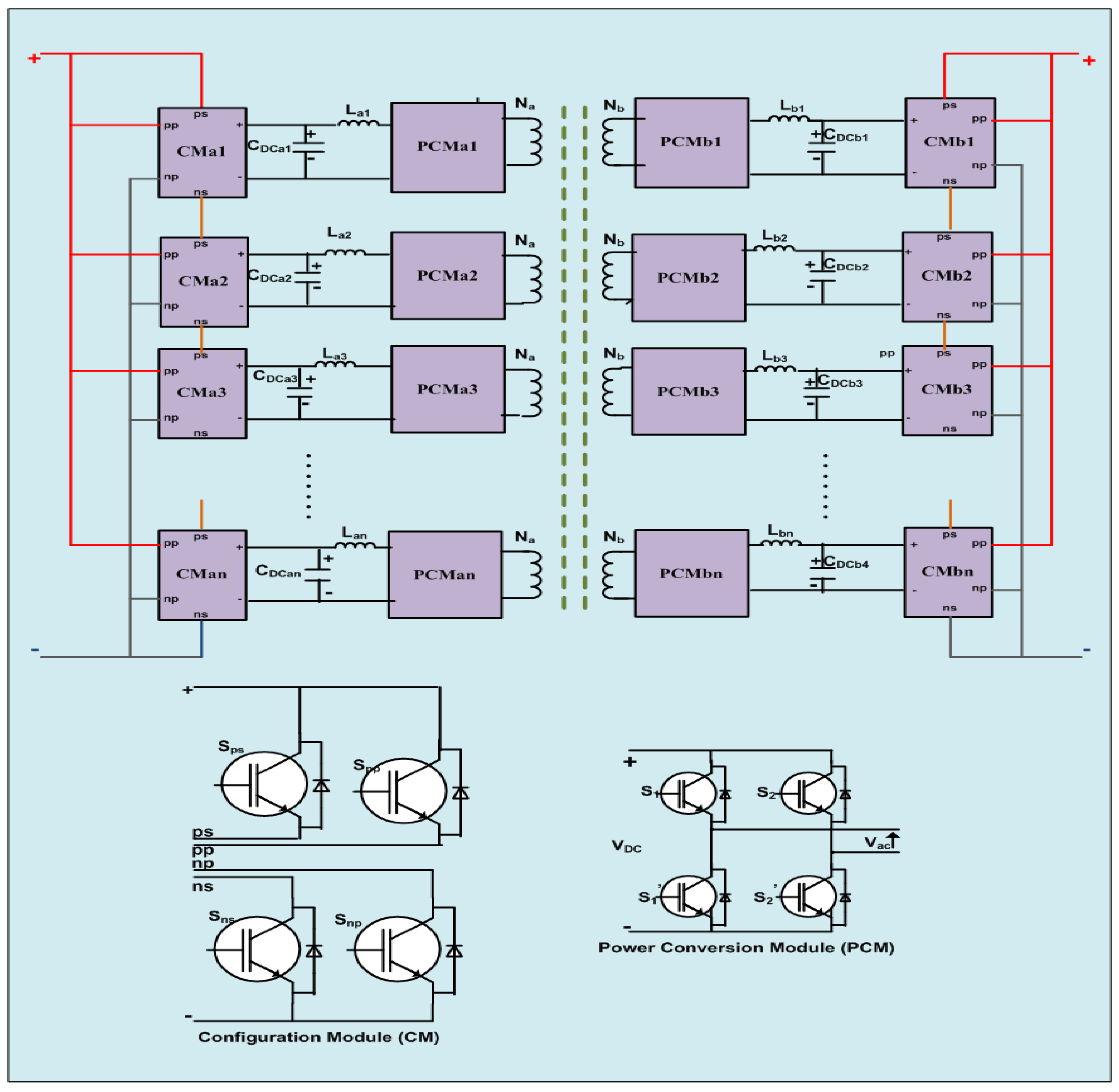
The configurable multiple winding DC-DC converter is essentially a group of dual active bridge (DAB) converters which share a common transformer core and whose connections are electrically configurable at primary and secondary sides. Each DAB consists of a power conversion module (PCM), configuration module (CM), DC link capacitor and filter inductor on each side of its windings. The PCM, as shown in Figure 1, is the basic H-bridge module with positive and negative DC rails across the DC link capacitor and AC port formed between poles points of H-bridge legs. The source-side PCM is current controlled for the required modulation index to supply designated power to load. The load side PCM is current controlled for the desired modulation index and phase shift to deliver designated power to load.
The configuration module, which is also depicted in Figure 1, is the key element which connects the respective sides of any DAB module in series or parallel to adjacent modules on either side. It consists of four independent switches, with two switches originating from the positive rail and the other two originating from the negative rail. Turning ON SPS connects it in series to the upper adjacent module. Turning ON SPP connects it in parallel to the upper adjacent module. With both the switches turned OFF, the module is isolated from the upper adjacent module. Similarly, turning ON SNS connects it in series to the lower adjacent module. And turning ON SNP connects it in parallel to the lower adjacent module. With both the switches turned OFF, the module is isolated from the lower adjacent module. Therefore, configuration modules of each DAB can configure the converter into series, parallel, series–parallel or multiple ports (independent loads) on either side of the transformer. Thus, the converter can be configured to convert power from a high-voltage source to low-voltage–high-current load or low-voltage source to high-voltage load. Also, multiple inputs and multiple outputs can be configured by suitable isolation of intermediate DAB modules. The switching combination of each CM for configuration choices of each PCM to adjacent PCMs are presented in Table 1.
The n-module DAB on the single-core transformer with stated power conversion and configuration modules on each side of the transformer is depicted in Figure 1. In the figure, Na represents the transformer’s turn towards the ports and Nb represents the transformer’s turn towards port b for each DAB. CDCxy forms DC link capacitors and Lxy form filter inductors for respective modules. CMxy forms configuration modules on each side of the DAB, which connect a module to adjacent modules in series or parallel or isolated, where x is a or b and y = 1, 2…n. Therefore, the proposed topology can configure n-parallel/series-connected modules, a series–parallel combination of modules, or multiple ports with a maximum of n-ports on either side. Thus, the DC-DC power conversion can be configured for n-series connected high voltage to n-parallel connected low voltage high current with interleaved operation or vice versa. Also, any number of sources less than or equal to n can be connected or maximum of n loads can be supplied with the proposed converter. Considering K as the transformer turns ratio of each DAB module where K = Na/Nb and VDC is the maximum allowable DC link voltage for each DAB module. Table 2 presents the possible combinations of loads which could be supplied by the converter for a wide range of source voltages.

2.2. Small Signal Model

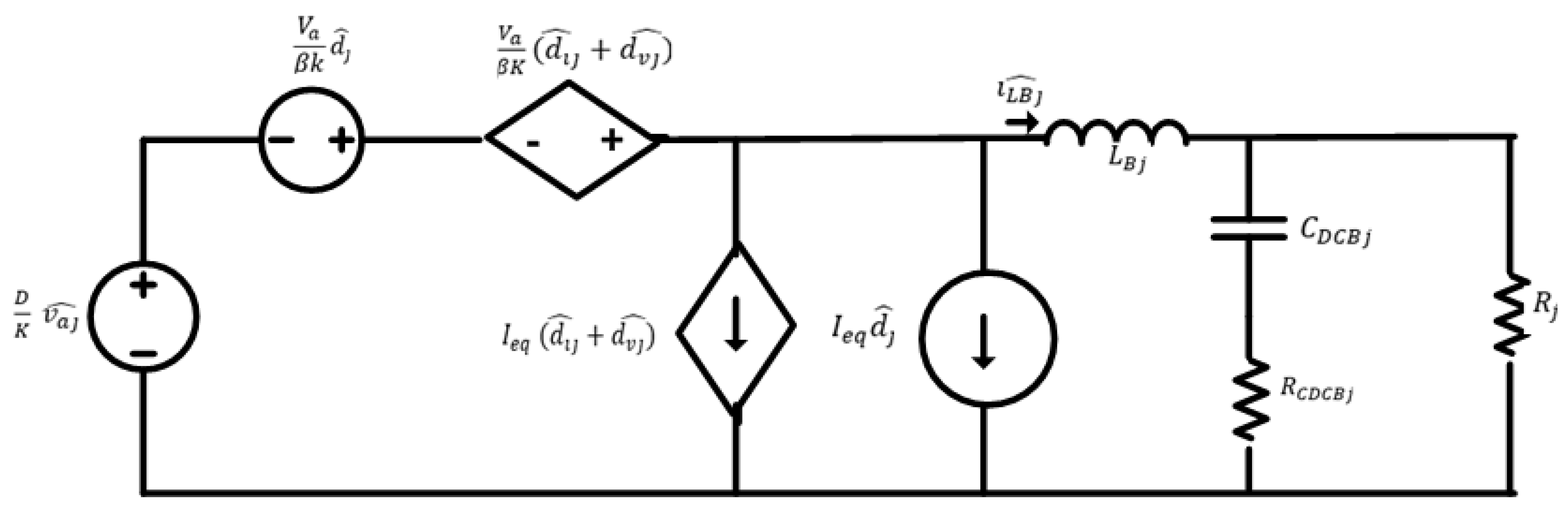
The analysis considers the converter as a group of n-DAB modules which are electrically configurable on either side of the transformer. Considering the operating modulation index and phase shift are obtained from the averaged model, the perturbations of the modulation index are determined through the following small signal model. Figure 2 depicts the small signal equivalent circuit for one isolated j-th DAB module where j ∈ [1, n]. The analysis considers the modules to be connected in series/parallel or series–parallel combinations to make one input port (port a) and one output port (port b). However, the same analysis is applicable for any number of isolated ports formed by the converter as per the required loads and available sources. The technical notations used in the figures representing small signal analysis are described as follows: α represents the power conversion module combinations connected in parallel at port a. k represents power conversion module combinations connected in parallel at port b. β represents power conversion module combinations connected in series along port a. γ represents power conversion module combinations connected in series along port b. The load RJ is equivalently determined based on series or parallel connection of modules. For total parallel combination, it is equal to the load nR. For total series combination, it is equal to R n . For series–parallel combination of modules, it is equal to γ R k . Similarly, the equivalent filter inductance LBJ and equivalent DC link capacitance CDCBJ are determined according to series/parallel configurations. Each module therefore contributes a current i L B j ^ which is the account of averaged modulation index D, voltage control and current control small signals at the respective instants of time. Thus, the instantaneous current contribution by each module is controlled by the voltage sources as a result of applied primary voltage at port a, instantaneous voltage control of load, and instantaneous current control of load. The voltage sources D K V a j ^ and V a β K d j ^ are averaged voltages induced in the load-side conversion module, and I e q d j ^ is the induced current owing to instantaneous modulation index and its small perturbation. The dependent voltage induced V a β K ( d i j + d v j ^ ) and dependent current I e q ( d i j ^ + d v j ) ^ are owing to the current control and voltage control at load side. The perturbation in the nominal current controlled duty cycle d i j ^ is determined in Equation (1), with the desired current contribution provided by closed-loop control. Here, V a ^ is the perturbation in input voltage, fs is the switching frequency, and Llk is the equivalent contribution of leakage inductance of the transformer per module. Similarly, the voltage-controlled duty d v j ^ owing to perturbations in module input voltage V C D C a j ^ is given in Equation (2). The dependence of duty contribution per module on series- and parallel-connected output modules is observed from the relation. The equivalent current induced in the module in terms of input port current I a and load R is depicted in Equation (3).
d i j ^ = 4 β L l k f s K V a ^ I L B j ^
d v j ^ = β k L l k D f s γ K 2 V a ^ V C D C a j ^
I e q = k L l k D f s γ β K R I a
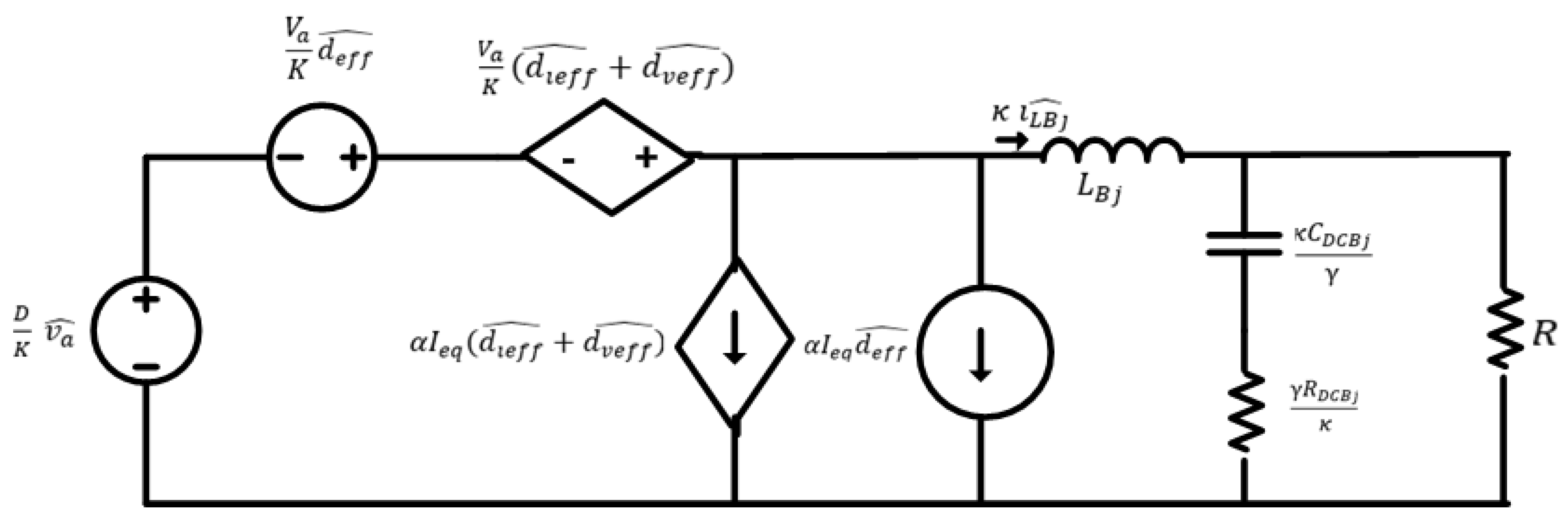
The equivalent small signal model for the proposed configurable converter is therefore the scaled version of the individual-module small signal model. The scaling factors include series and parallel combinations of modules on source side and load side. They are presented in Figure 3. The total indued voltage is now D K   v a ^ , and the small signal voltage is V a K d e f f ^ where d e f f ^ is the equivalent perturbation in the nominal modulation index combined for all modules. Similarly, α I e q d e f f ^ is the induced current owing to the instantaneous modulation index and its combined perturbation for all modules. The dependent voltage induced is now V a K ( d i j + d v j ^ ) and dependent current α I e q ( d i e f f ^ + d v e f f ) ^ , which are owing to the perturbations in modulation indices combined for all modules owing to current control and voltage control at load side. For k parallel module combination at load side, the equivalent current supplied is k i L B j ^ . With these developed voltages and currents in the overall modules, KVL and KCL in the equivalent circuit of Figure 3 determine the circuit parameter relations for input voltage, load voltage, input current and load current. These are depicted from Equations (4)–(7).
Applying KVL across the outermost loop in Figure 3 results in Equation (4) and its equivalent configurable modules for k parallel current contributions at load side, and Figure 3 also presents results from Equation (5).
D K   v a j ^ + v a β K ( d i j ^ + d v j ^ + d j ) ^ = s L i L j ^ + v b j ^
D K   α v a ^ + v a β K j = 1 n ( d i j ^ + d v j ^ + d j ) ^ = ( s L   j k   i L j ^ ) + i k   v b i ^
Applying KCL at output node results in Equation (6) and its equivalent configurable module scaled version seen in Figure 3, resulting in Equation (7) and neglecting the series resistance of DC link capacitors.
i L B 1 j ^ + i L B 2 j ^ + i L B 3 j ^ + + i L B n j ^ = s C D C B J s C D C B J R D C B J + 1 v b j ^ + v b R ^
i = 1 γ j = 1 k i L B i j ^ = s C v b ^ + k v b ^ R
where v a j ^ , v b j ^ are perturbed voltages per module at input and output side, and v b j ^ is the overall port b voltage perturbation.

2.3. Control Transfer Functions

This section evaluates the control transfer function which aids closed-loop control design. The suffix eff is omitted from the overall combined modulation index perturbation for simplicity. Substituting for d i j ^ and d v j ^ from Equations (1) and (2) in Equation (5) results in Equation (8); rearranging it determines the voltage control transfer function as depicted in Equation (9).
D K   α v a ^ + v a β K j = 1 n ( 4 β L l k f s K v a I L B j ^ + β k L l k D f s γ K 2 v a V C D C a j ^ + d ^ ) = ( s L   j k   i L j ^ ) + γ v b ^
  v b ^ d ^ = v a β K ( s C + 1 ) L C s 2 + k L R + 4 L l k f s K 2 C s + k 4 L l k f s K 2 R + γ
To determine the current control transfer function, input voltage perturbations are neglected. Rearranging Equation (7) into Equation (10) and substituting in Equation (8) with input voltage perturbations V C D C a j ^ and v a ^ , reducing to zero as depicted in Equation (11), results in the current control transfer function as presented in Equation (12).
i = 1 γ j = 1 k i L B i j ^ = s R C + k R v b ^
v a β K d ^ v a β K j = 1 n 4 β L l k f s K v a I L B j ^ = ( s L   j k   i L j ^ ) + γ R s R C + k j = 1 n i L B j ^
i L ^ d ^ = v a β K ( s R C + k ) R L C s 2 + k L R + 4 L l k f s K 2 C s + k 4 L l k f s K 2 R + γ
To determine the small signal voltage-gain modulation index, perturbations are neglected. Rearranging Equation (8) with d ^ , reducing to zero as depicted in Equation (13), and substituting for j k   i L B j ^ from Equation (7) simplifies it to the relation between input and output voltage small signals as shown in Equation (14). Transforming Equation (14) to determine the voltage gain v b ^ v a ^ is depicted in Equation (15).
D K   α v a ^ + v a β K j = 1 n ( 4 β L l k f s K v a I L B j ^ + 4 β k L l k D f s γ K 2 v a V C D C a j ^ ) = ( s L   j k   i L B j ^ ) + γ v b ^
D K   α   ( 1 + k 4 β L l k f s γ R K )   v a ^ = ( s L + 4 β L l k f s K 2 ) ( s R C + k R )   v b ^ + γ v b ^
v b ^ v a ^ = D K   α   ( 1 + 4 k β L l k f s γ R K )   L C s 2 + k L R + 4 L l k f s K 2 C s + k 4 L l k f s K 2 R + γ
Also, the output impedance of the converter is obtained by neglecting control-independent input voltages and output current. Therefore, Equation (7) is rearranged with input voltage and output current perturbations reducing to zero as in Equations (16) and (17); substituting in Equation (8) results in Equation (18), and rearranging it to obtain the output impedance of the converter is shown in Equation (19).
i = 1 γ j = 1 k i L B i j ^ = s C v b ^ + k v b ^ R   k i b ^
i = 1 γ j = 1 k i L B i j ^ = ( s R C + k R )   v b ^   k i b ^
v a β K j = 1 n ( 4 β L l k f s K v a I L B j ^ ) = ( s L   j k   i L j ^ ) + γ v b ^
Z b = v b ^ i b ^ ^ = k ( s L + 1 4 β L l k f s K 2 v a ) L C s 2 + k L R + 4 L l k f s K 2 C s + k 4 L l k f s K 2 R + γ

2.4. Multiple Output Port Mode Power Transfer

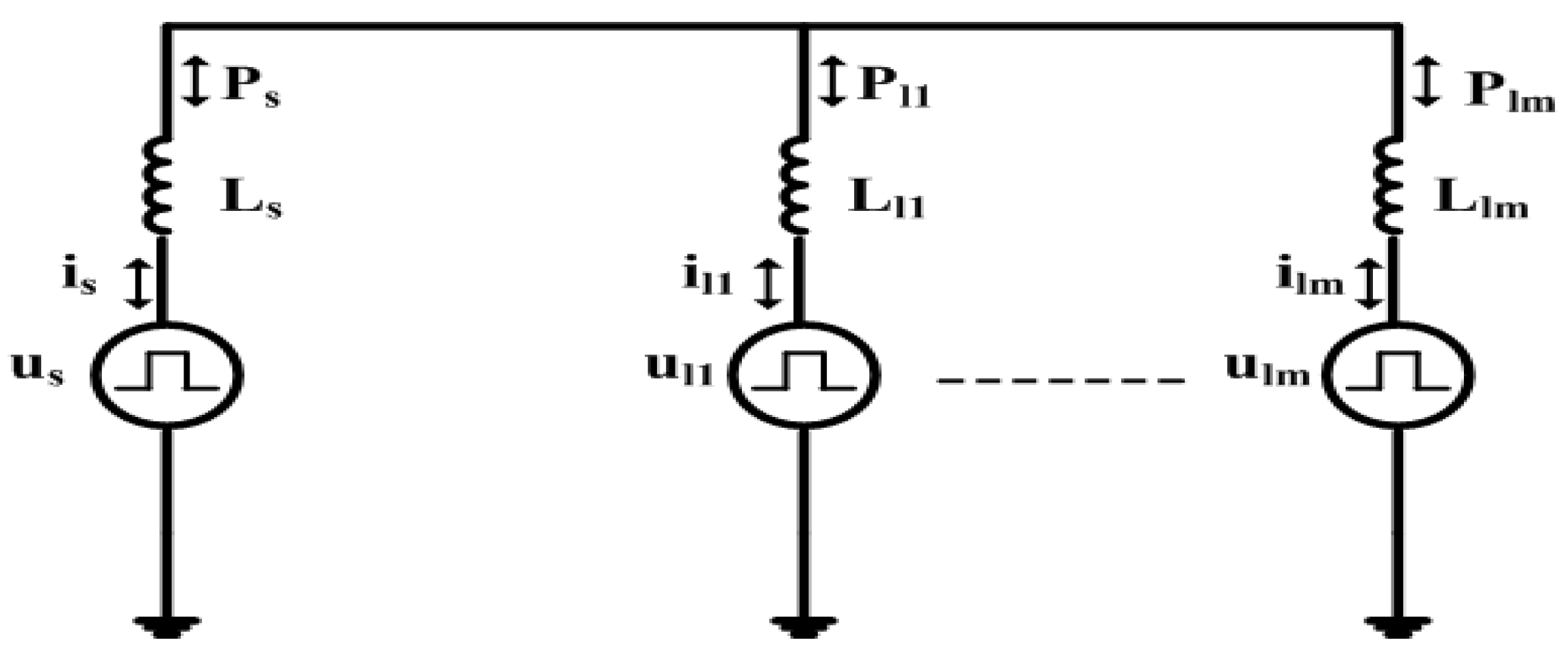
The analysis of the converter presented in the previous sub-section aids closed-loop control design. Further, for the design of possible multiple-port power transfer with the proposed converter, the steady-state power delivery to various loads configured under multiple output configurations is presented in this sub-section. The transferred power is presented at AC terminals of various ports formed by the configurable converter. Let the AC equivalent voltage of input port be us supplying power to m-number of load ports with the respective AC equivalent voltages as ul1 to ulm. The AC powers associated with various ports are represented in Figure 4, which depicts the developed AC voltage through interconnecting equivalent inductance delivering or absorbing power from the transformer core. Each load port is associated with power Plx through the interconnecting inductor Llx. The power delivered by input port through the interconnecting inductor Ls is designated as Ps.
The square wave voltage developed across the AC output port of source power conversion modules is given as
u s = k = 1,3 , 5 4 V a k π c o s k α s 2 sin ( k ω s t )
where α s is the ON duration in radians per half cycle, ω s is the switching frequency in rad/s, and V a is the input DC voltage.
The square wave voltage developed across the AC output port of the xth load power conversion module is given as
u l x = k = 1,3 , 5 4 V a V b x k π c o s k α x 2 sin ( k ω s t + k ϕ x )
where α x is the ON duration in radians per half cycle, ϕ x is the phase shift between the source module AC voltage and respective load converter module AC voltage, and V b x ′ is the source-referred AC equivalent voltage of the load converter module AC voltage.
The power delivered to load modules AC ports is therefore obtained as in Equation (22), and the total power delivered by the source is algebraic sum of powers delivered to load ports is given in Equation (23).
P l x = k = 1,3 , 5 8 V d c x k 2 π 3 X e q x c o s k α s 2 c o s k α x 2 sin ( k ϕ x )
P s = k = 1,3 , 5 P l x

3. Converter Control

The closed-loop control of the proposed configurable converter to meet the desired load characteristics is implemented through outer voltage loop and inner current loop control. Firstly, the configuration modules are programmed to arrange necessary electrical connections of DAB modules on either side of the transformer based on the source and load voltages and currents. The control parameters for outer and inner PI controllers are also determined by the configuration control module.
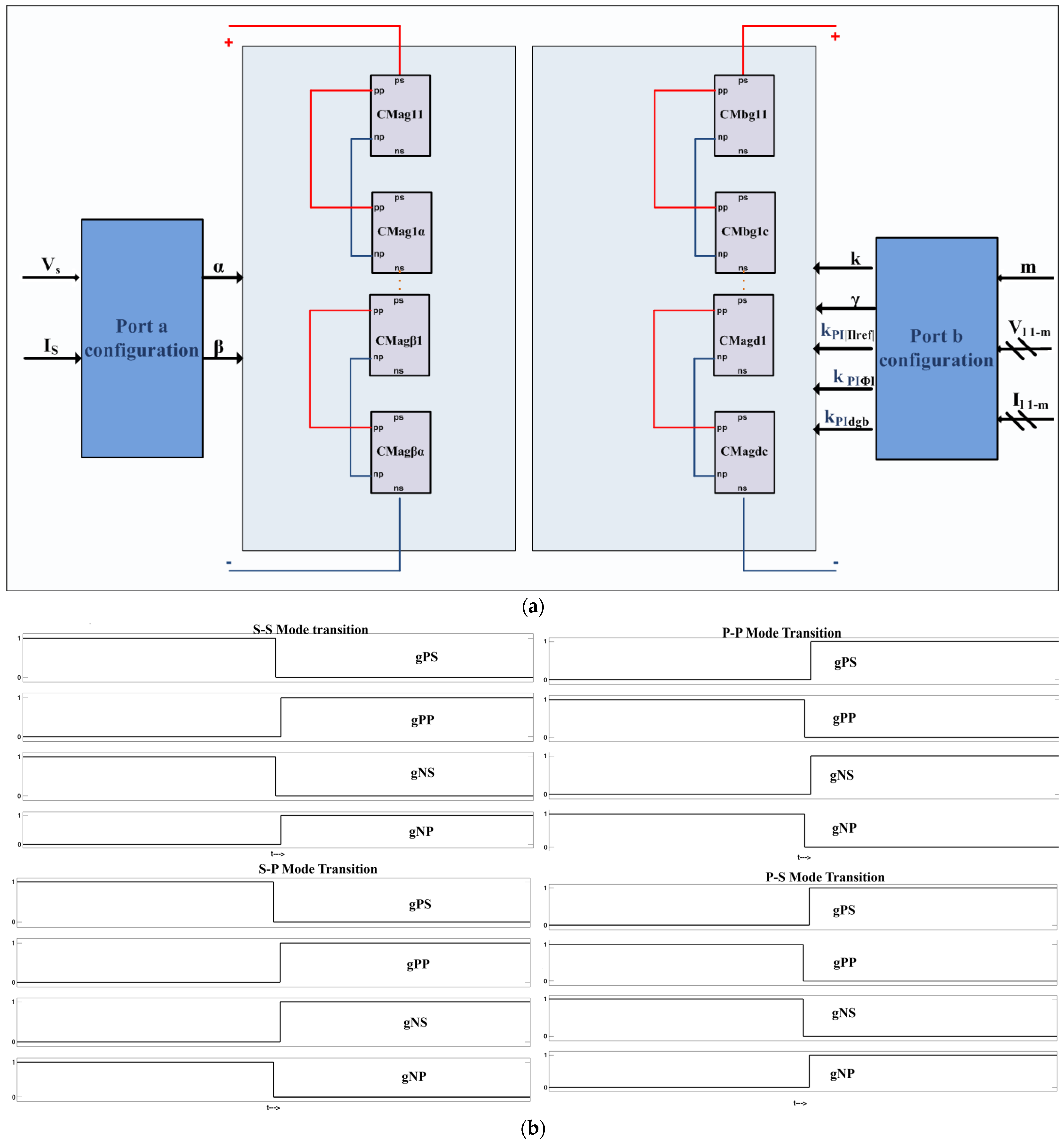
Later, output voltage and current regulation closed-loop control regulates currents delivered by individual DAB modules to meet the required load characteristics. These aspects are detailed as follows. Figure 5a depicts the on-load converter configuration and control parameter programming scheme. Nominal values of source voltage and current, number of load ports, and voltage and current of each load are inputs to program the electrical connections and determine PI controllers’ constants. The number of load ports configure groups of parallel modules, series connection of module groups, and isolated modules to form each port. Simultaneously, the PI controller constants for voltage loop, phase shift determination and module group current controllers are set by the algorithm.
At the input side, VS and IS determine parallel module group α and series connection of such module group β. At the load side, number of load ports m and their respective nominal voltages and currents Vl 1−m, Il 1−m determine parallel modules at load side k, series connections of such modules γ.
Following the mode determination, the corresponding transition is implemented by respective CMs. The sequence of switching operations of PS, PP, NS, NP switches in the ith CM during on-load reconfiguration is depicted in Figure 5b for four possible transitions viz. series to upper and lower adjacent modules (S-S), parallel to upper and lower adjacent modules (P-P), series to upper adjacent modules and parallel lower adjacent modules (S-P), parallel to upper adjacent modules, and series to lower adjacent modules (P-S). The CM switches are operated in a predefined non-overlapping sequence as shown in Figure 5b to ensure a safe transition between operating modes. Before establishing a new current path, the previously conducting CM switch is turned OFF and a short interlock interval is provided to avoid simultaneous conduction. Subsequently, the required CM switch for the target configuration is turned ON, thereby completing the transition. This sequence minimizes the possibility of shoot-through and circulating-current paths during reconfiguration.
The number of series connected modules is the function of source voltage which is given as
β = V s V D C
where Vs is the required source voltage and VDC is the nominal voltage of each DAB module on primary side.
Similarly, the number of parallel connections for each of series connected module groups is obtained as
α = I s I D C
where Is is the required source current and IDC is the nominal current of each DAB module at source terminals which holds only for n 2 β .
On the load side, it is the number of loads, voltage and current required at each load terminal the determines the parameters k and γ. For single-load port configuration, the number of series connected modules at load side are
γ = K V l V D C
where Vl is the required load voltage. Similarly, the number of parallel connections for each of series connected module groups is obtained as
k = I l K I D C
where Il is the required source current and IDC is the nominal current of each DAB module at source terminals which holds only for n 2 γ .
For multiple-load-port configuration, the number of series connected modules per load are
γ = K V l m V D C
where Vl is the required load voltage and m is the number of loads. Similarly, the number of parallel connections for each of series connected module groups per load is obtained as
k = I l m K I D C
which holds only for n 2 γ / m .
Also, the constants for PI controllers are selected for obtained converter configuration based on m, k and γ which are set following the design Equations (1)–(7), pertaining to equivalent load voltage and current per module referred to source side. The aspects are summarized in Equations (24)–(29), which provide the configuration of modules, and Table 3, which provides the configuration of control parameters.
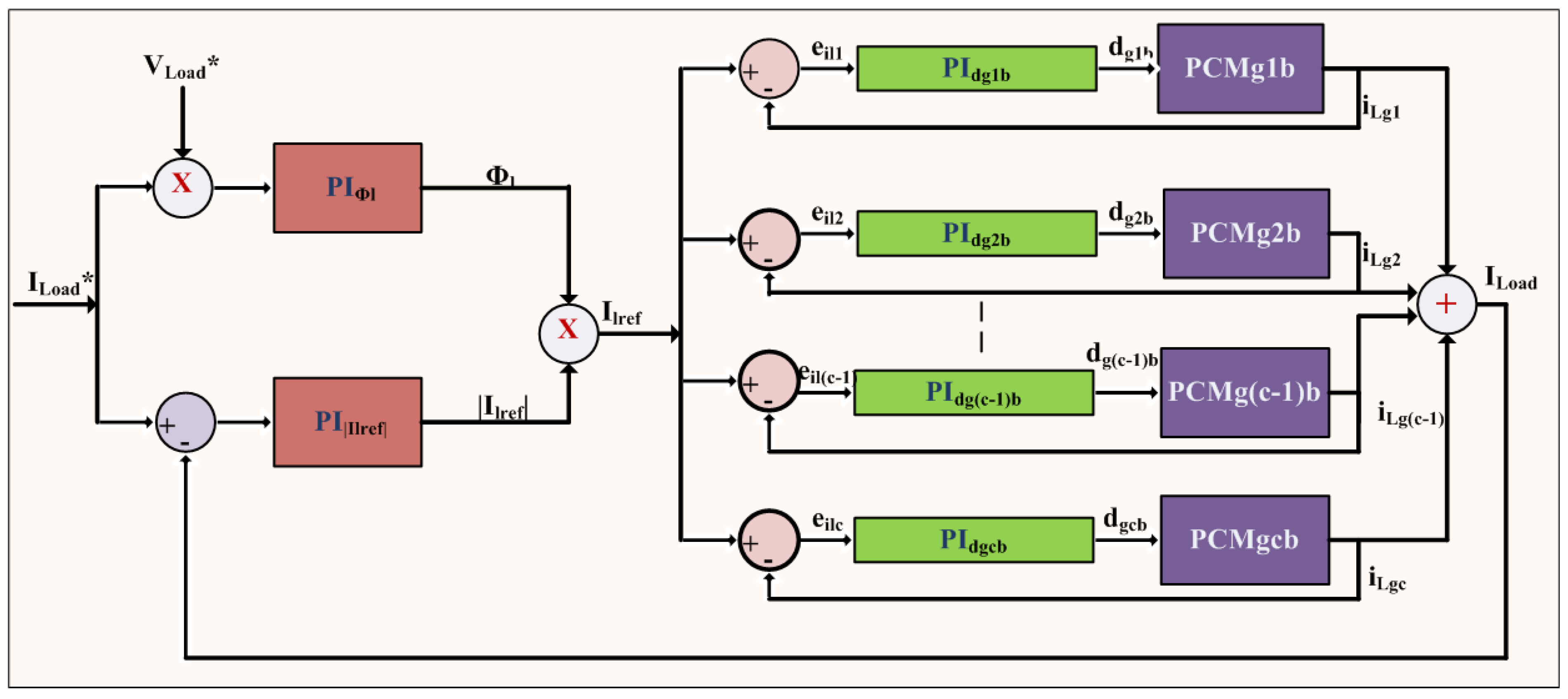
The closed-loop control for current control for filter inductors of load-side PCM groups is depicted in Figure 6. The reference load voltage ad current determines the load power, which is supplied to PIϕl for each load to determine the respective phase shift in the current with respect to source-side AC current. Simultaneously, the error in reference and actual load currents supplied to PI|Ilref determines the magnitude of reference current magnitude for an individual filter inductor formed by parallel PCM groups at load side. The product of inductor current reference with phase shift determines the instantaneous reference current for each of the parallel PCM groups. These reference currents are compared to actual inductor currents, the error of which is provided to duty regulate PI controllers PIdg1b–PIdgkb, which provide instantaneous duty cycles for respective PCM power switches. The control structure is scaled for control parameters setting as depicted in Table 4, and multiple simultaneous loops are implemented for respective port voltage and current references for multi-port configuration of the converter.

4. Simulation and Experimental Results

Simulation and experimentation were carried out for configurable 2-module DAB converter with resistive loads. Simulation results for steady-state and transient conditions under series or parallel or multi-port operations were recorded and analyzed. The source, load and configuration parameters for simulation and experimental study are shown in Table 4.
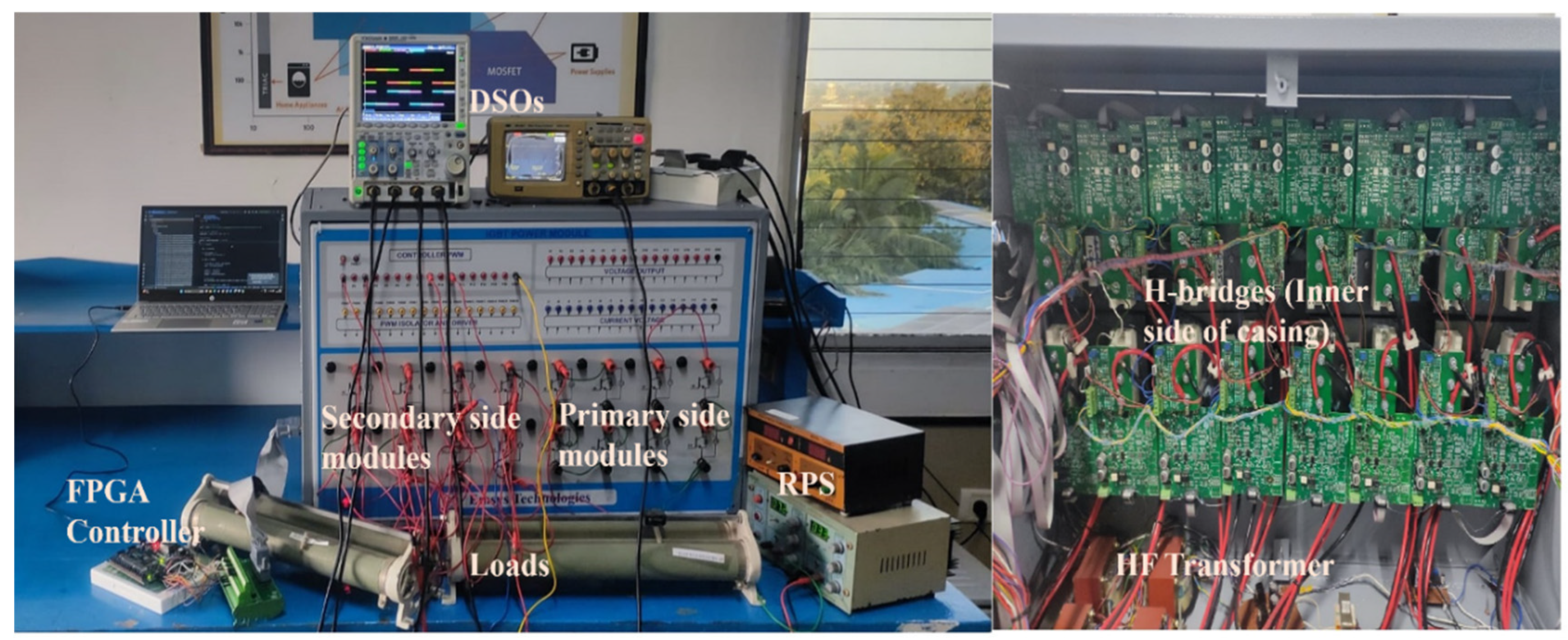
Simulation and experimental studies were performed in the following sequence. First, series output mode command is implemented, followed by parallel output mode command, and finally, individual output mode command is implemented. For the simulation study, the mode switch is programmed for every 2 s. For the experimental study, a user button is provided to select the output mode. Experimental setup is shown in Figure 7, which presents two DAB modules connected through a multi-winding high frequency transformer, resistive loads, FPGA controller, RPS and DSOs.

4.1. Simulation Results

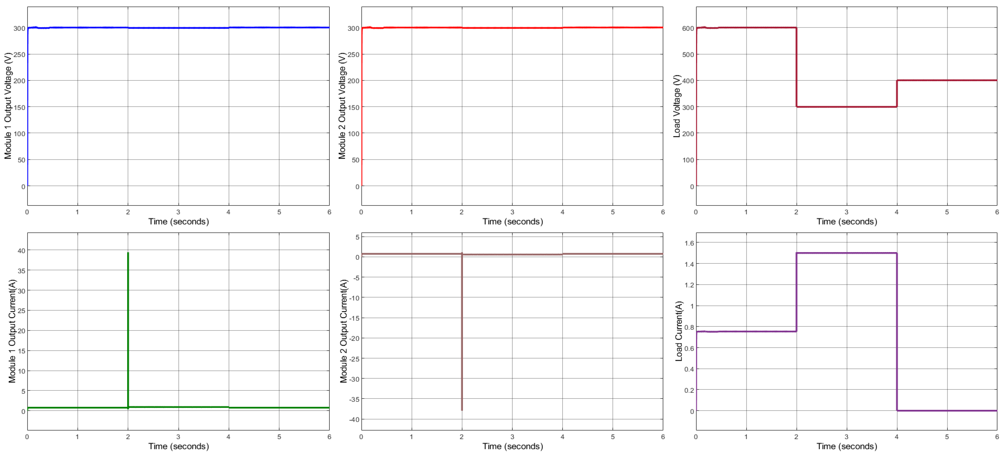
The overall simulation result for output module voltages and currents pertaining to all commands is presented in Figure 8. The feasibility of on-load configuration can be verified from it through the observed smooth switching of load with minimal current overshoot. The individual steady state and transient observations are presented in the successive figures.
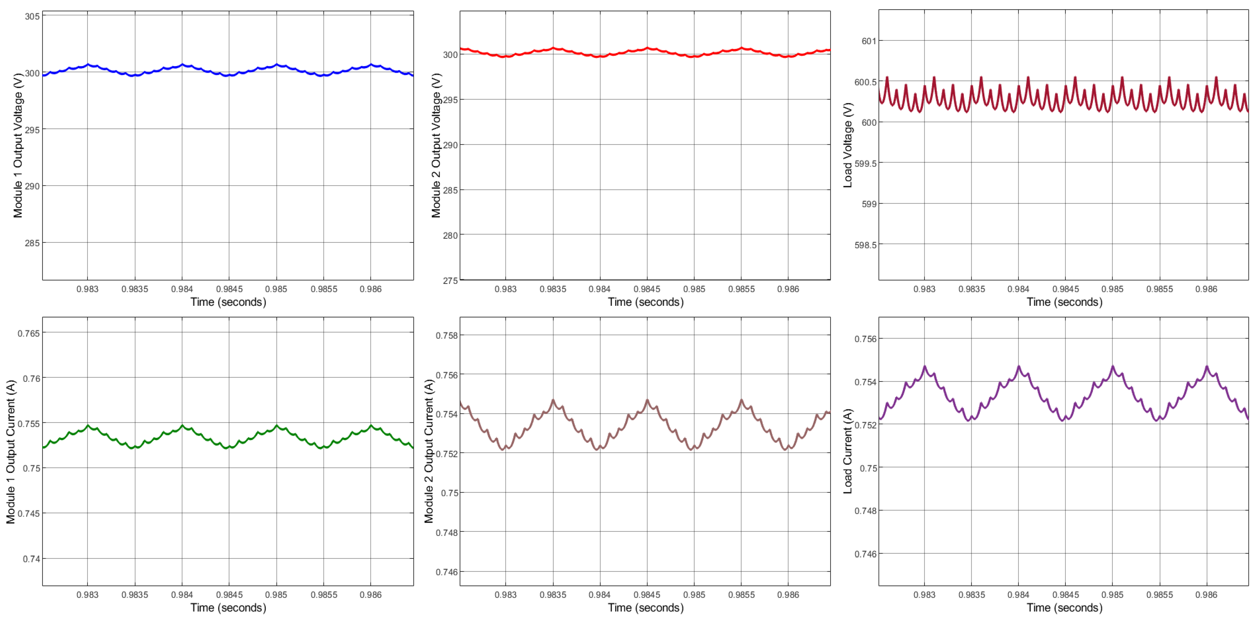
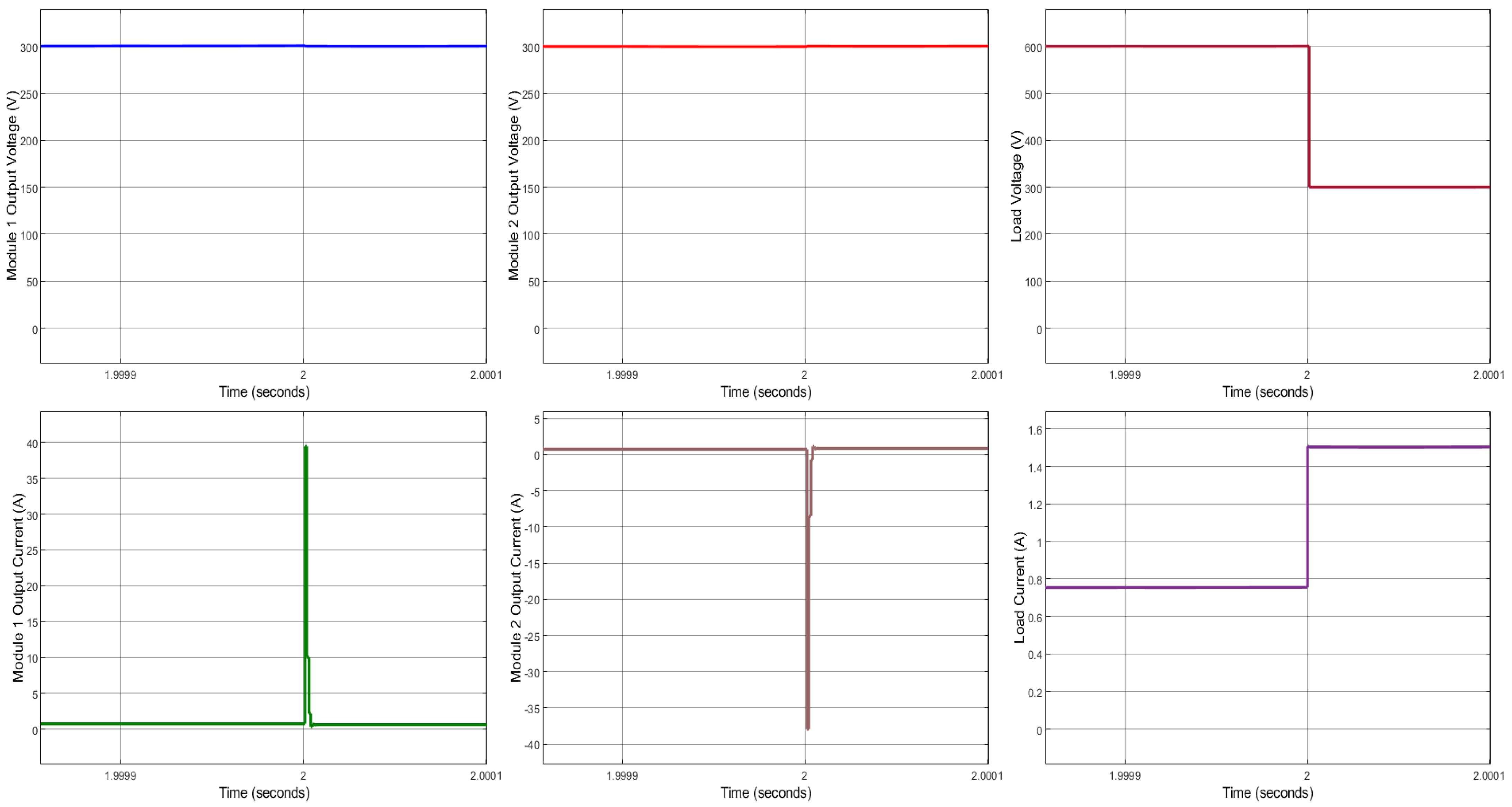
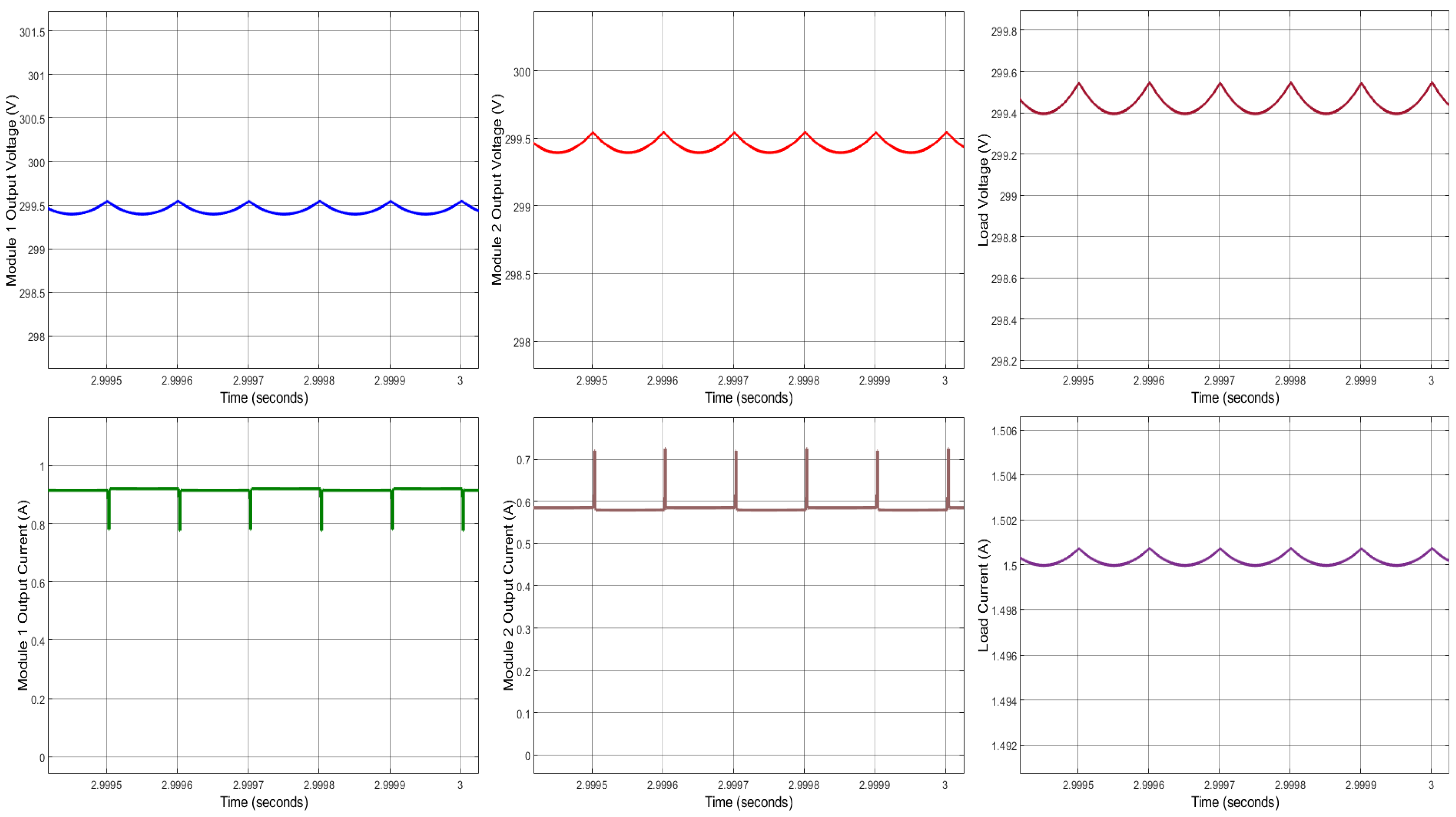
Figure 9 presents the simulation results for steady-state voltage and current at output terminals, individual modules, and series-connected load. The obtained steady-state values for individual module output voltages of 300 V and load voltage of 600 V verify the steady-state series operation of modules. The respective currents verify the feasible closed-loop current regulation. Figure 10 presents the transient condition for switching from series mode to parallel mode at t = 2 s. It is observed that while there is no change in individual module output voltages, the load voltage is changed to 300 V from 600 V owing to on-load configuration switch at output modules, which is accompanied by overshoot in current to 40 A. Since the converter operates at 5 kHz, the transient duration is less than one switching period (<200 μs). The resulting I2t stress is approximately 0.32 A2s, assuming an IGBT on-state voltage of 2 V. The energy dissipated during the transient phase is approximately 0.016 J. This corresponds to an estimated junction temperature rise of less than 0.2 °C, which is negligible compared with the allowable junction-temperature excursion of commercial 1200 V IGBTs.
Such a transient phase is significantly shorter than the thermal time constants of the semiconductor junction and lies within the pulse-duration region governed by the device’s transient thermal impedance. Consequently, the corresponding junction temperature excursion is negligible and remains well within the safe operating area of the employed IGBT. Therefore, although a brief current spike is observed during reconfiguration, its short duration and low energy content do not impose significant thermal stress on either the switching devices or the load. Figure 11 presents the simulation results for steady-state voltage and current at output terminals for individual modules and parallel connected load. The obtained steady-state values for individual module output voltages of 300 V and a load voltage of 300 V verify the steady-state parallel operation of modules.
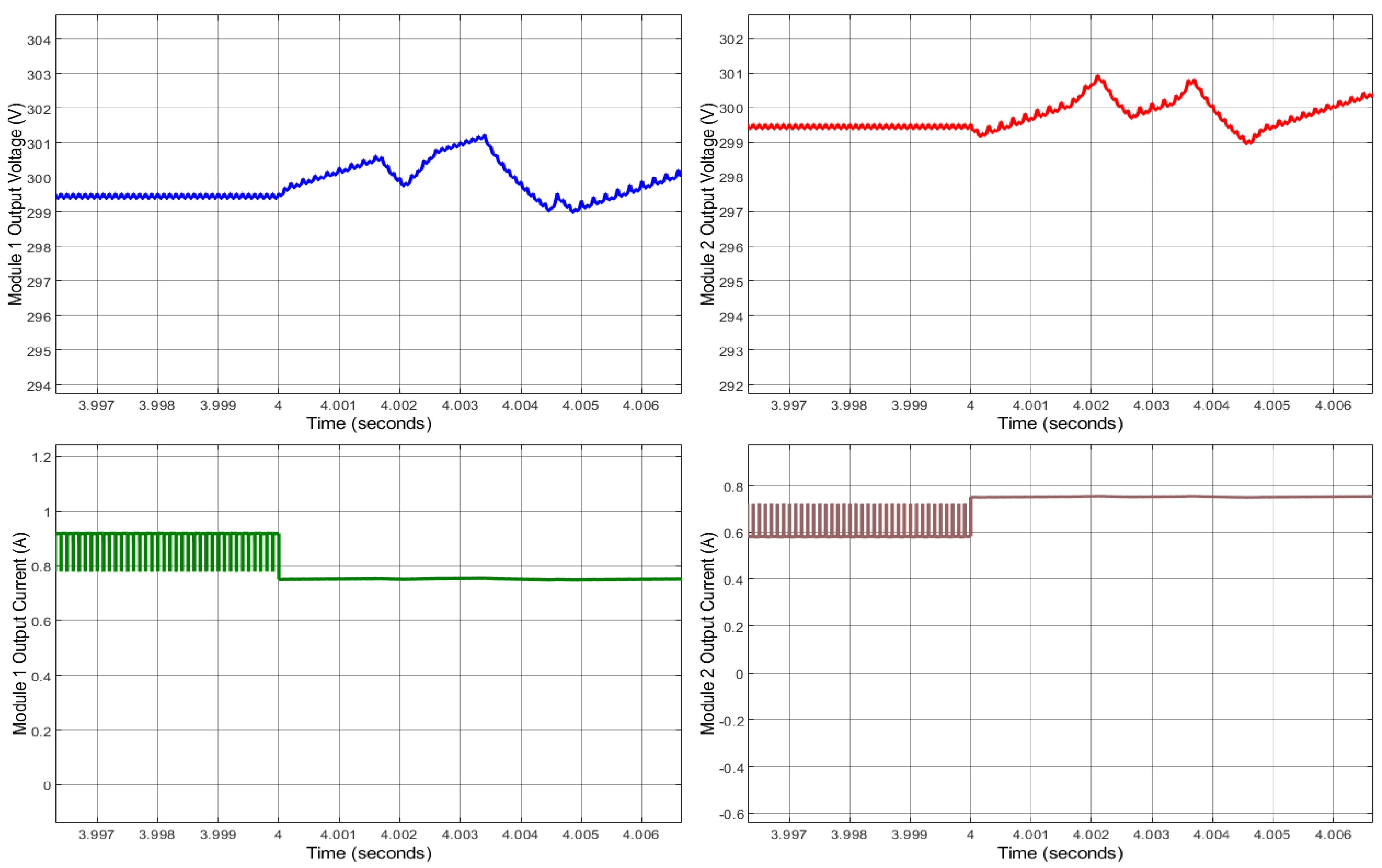
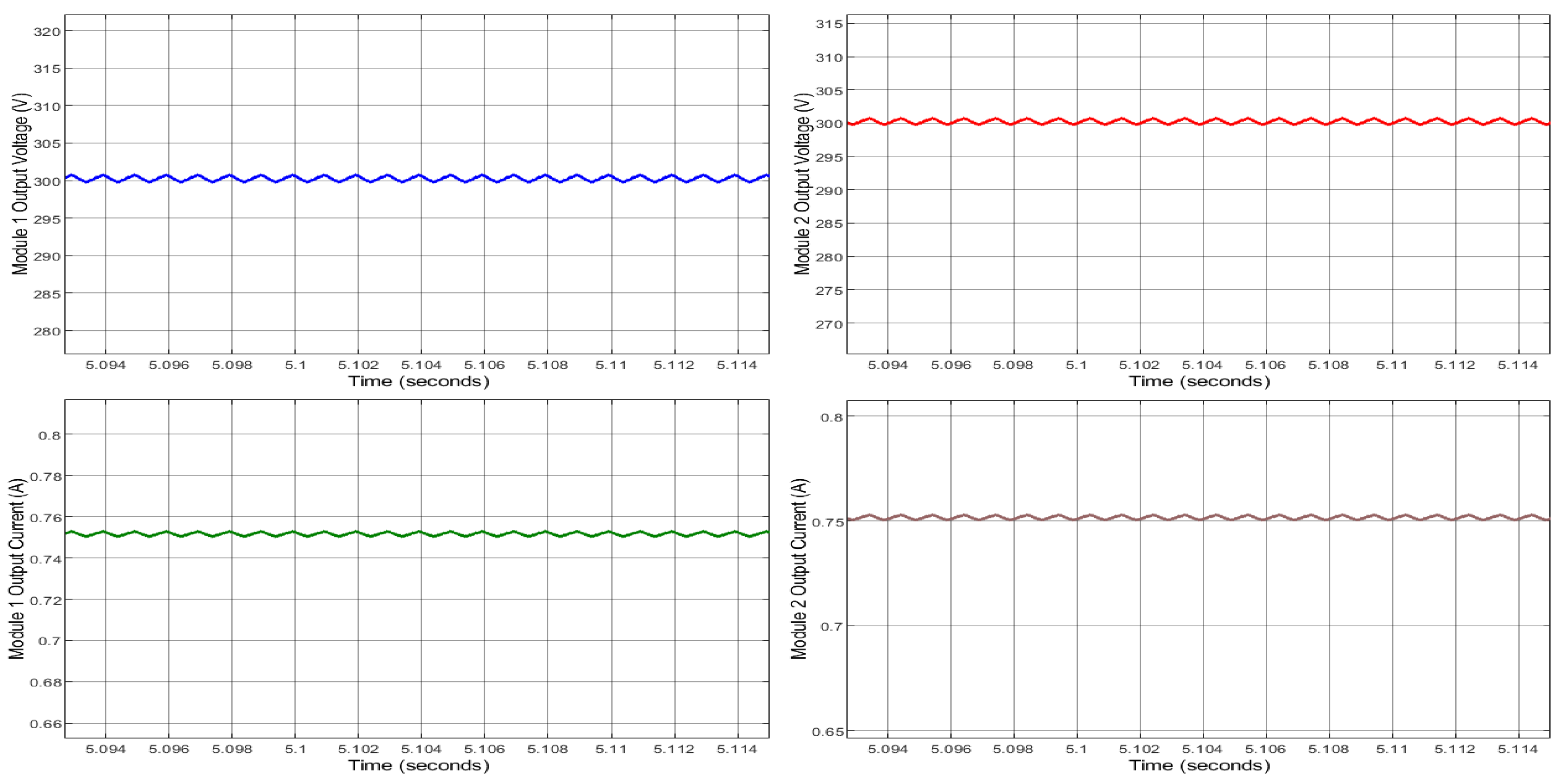
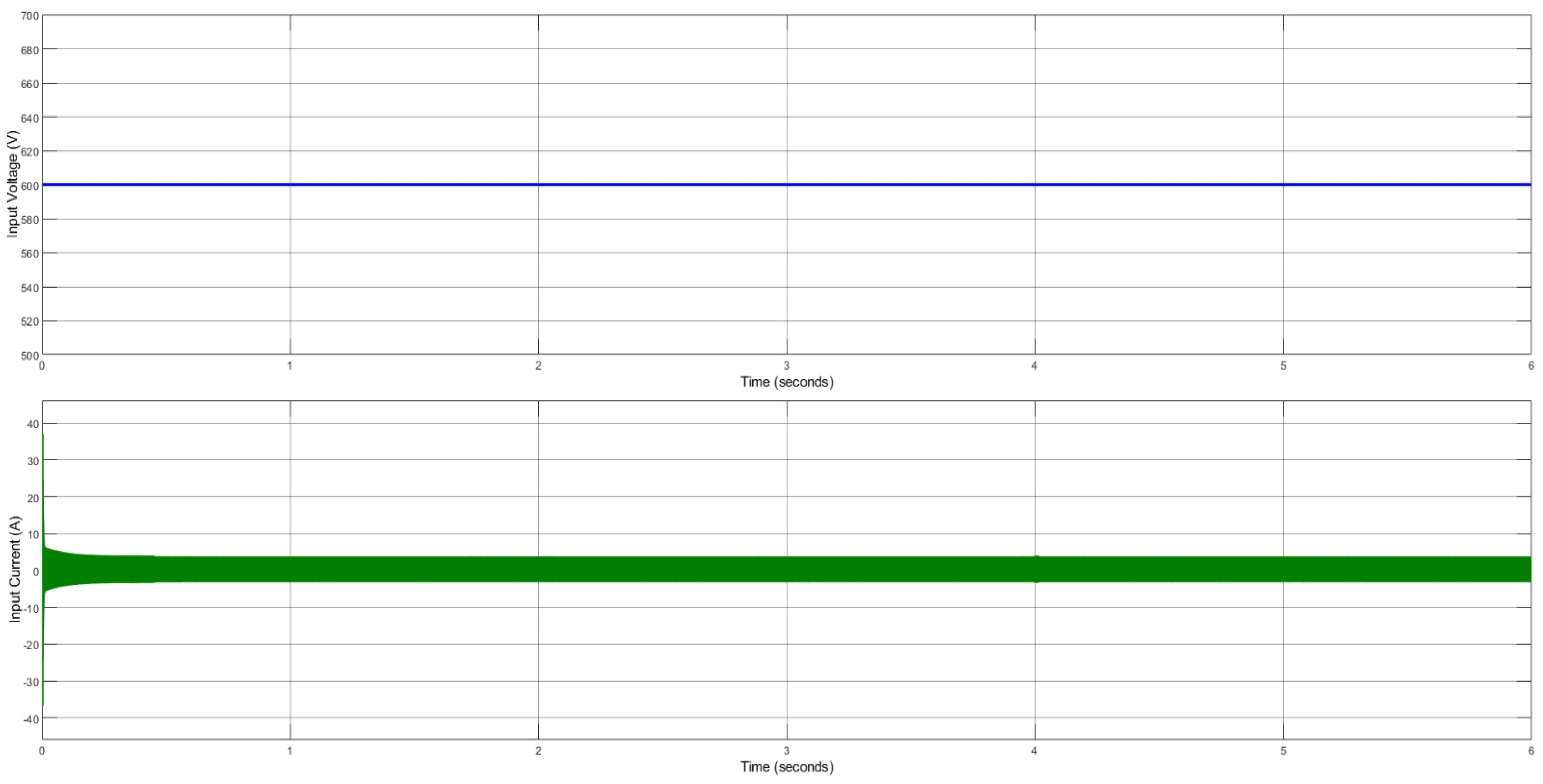
Figure 12 presents the transient condition for switching from parallel mode to independent load mode at t = 4 s. It is observed that, owing to the disconnection of modules, the interruption in voltages and currents is observed for 3 to 4 switching cycles and is restored back to 300 V. Figure 13 presents the simulation results for steady-state voltage and current at output terminals and individual modules during independent load operation. The obtained steady-state values for individual module output voltages of 300 V and respective currents verify the feasible closed-loop current regulation. For the overall duration, Figure 14 presents the stable voltage and current delivered by the DC source.
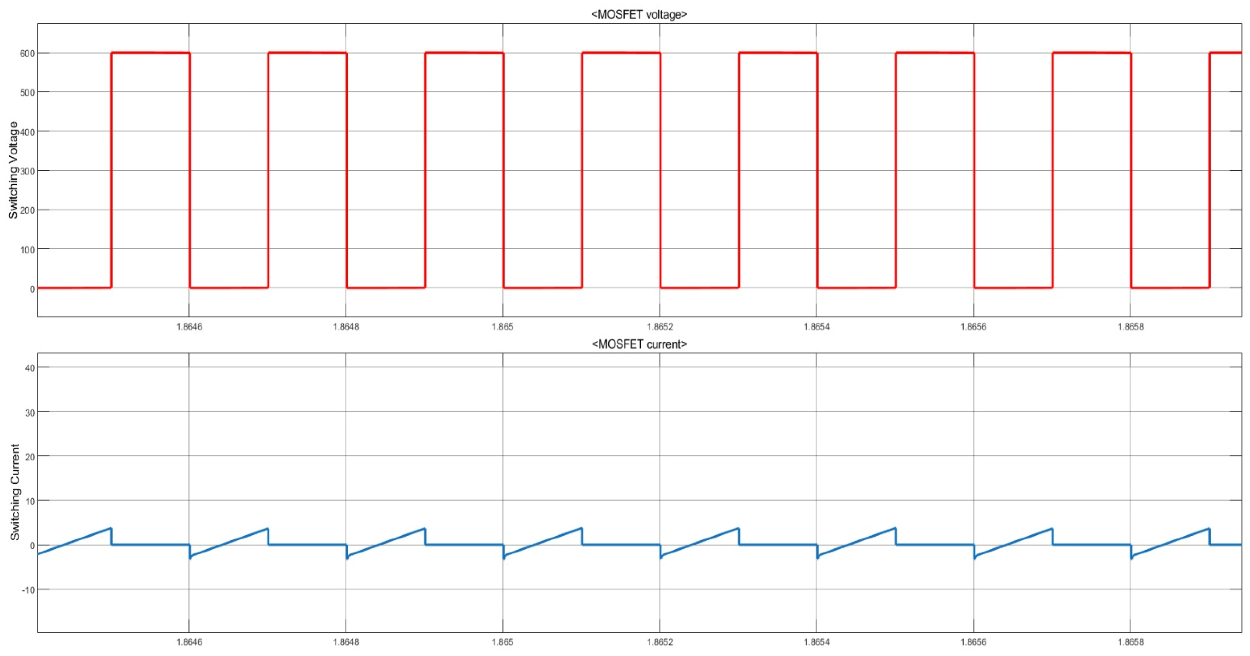
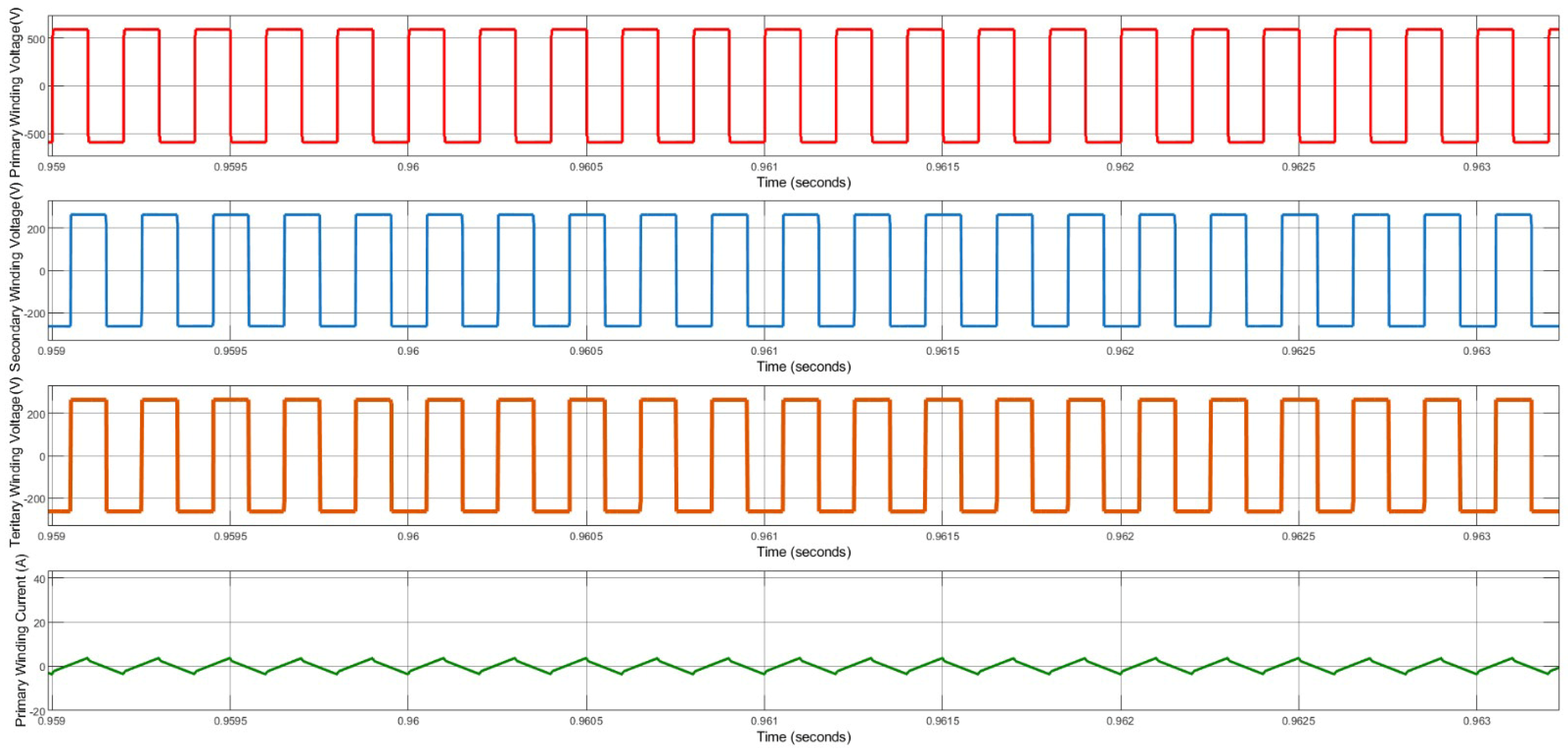
Figure 15 presents a few steady-state cycles of transformer winding voltages and primary side currents, which verify the stable DAB operation. Figure 16 presents a few steady-state cycles of one power switch voltage and current, which depict the nominal voltage and current through the switch. Also, it can be observed that there is no additional overshoot of voltage or current during mode switching.

4.2. Experimental Validation

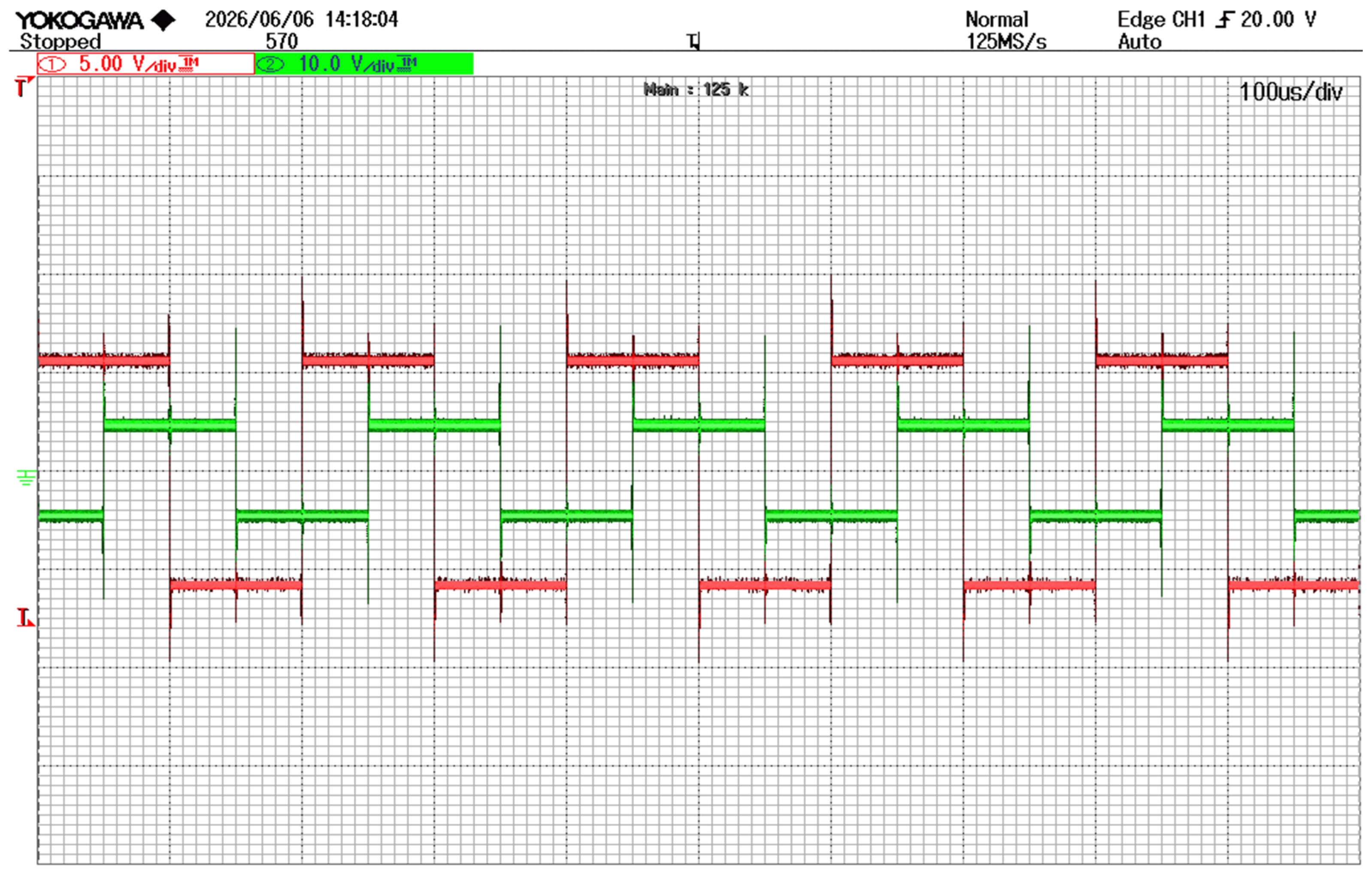
The experimental study is also carried out in a similar way to the simulation study. A 60 V DC source is considered while all other parameters are the same as those that are used for the simulation study. LV-25 and LA-25 Hall effect sensors are used for sensing voltages and currents, respectively. The sampling of measured voltages and currents is well above the switching frequency owing to the analog measurement of sensors. This ensures sufficient bandwidth for controller implementation. Artix-7 FPGA with VHDL programming provides the necessary on-load configuration and closed-loop current regulation. User-programmable switches set the mode of operation. A look-up table is implemented for converter configuration parameter determination upon operation mode command as per Table 3. Further, these are communicated into another VHDL file which simultaneously implements digital PI controllers as per the control scheme presented in Figure 6.
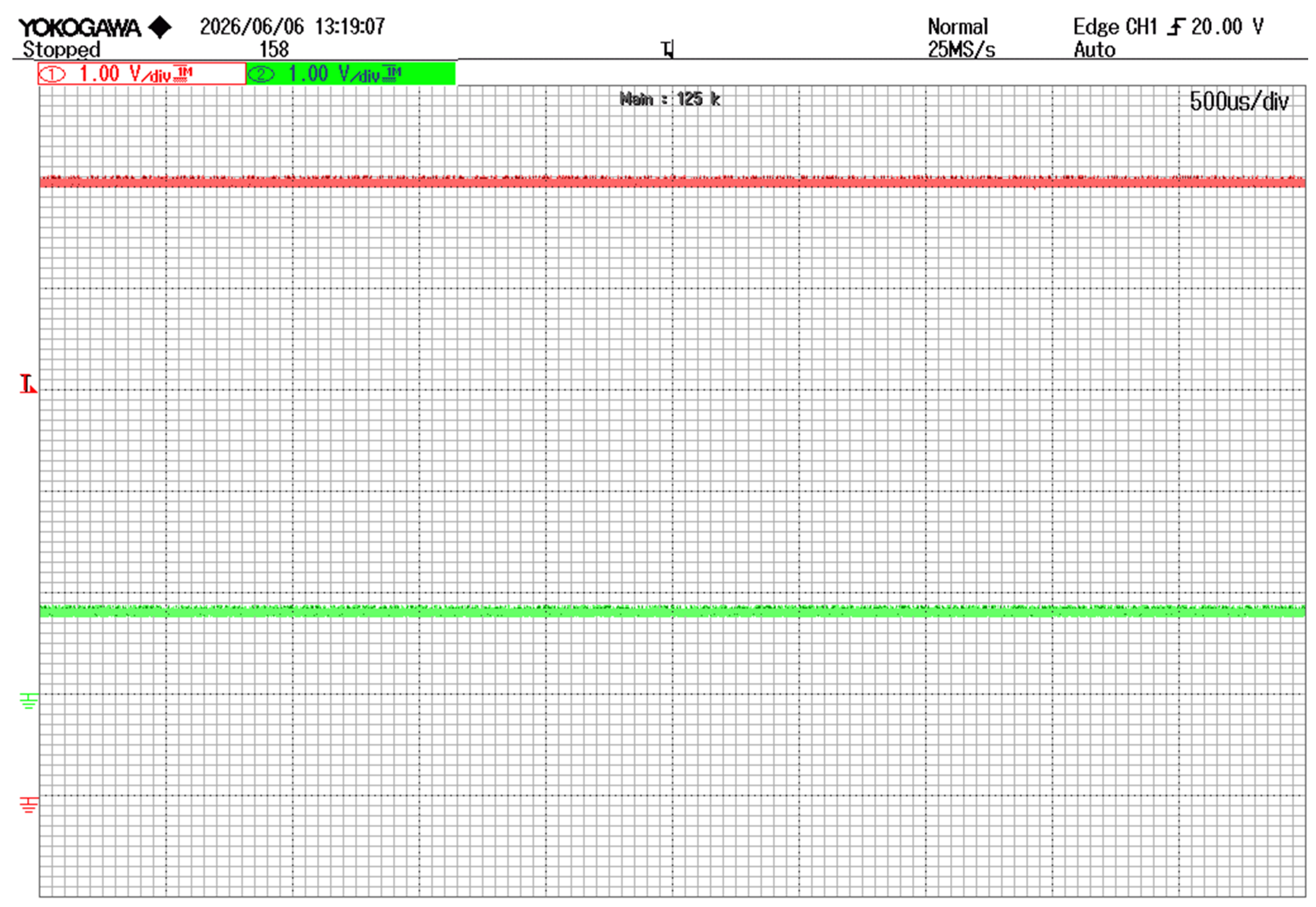
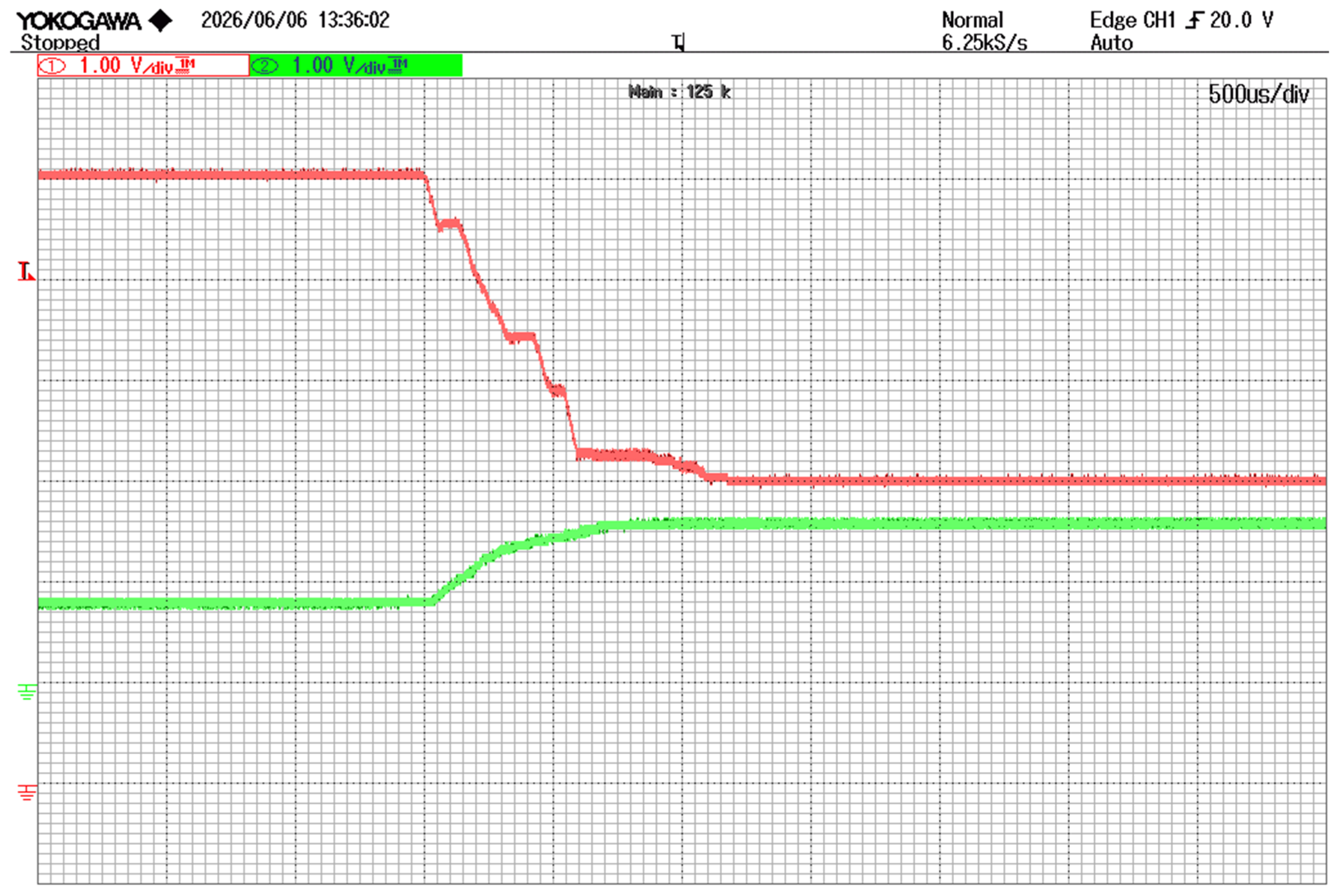
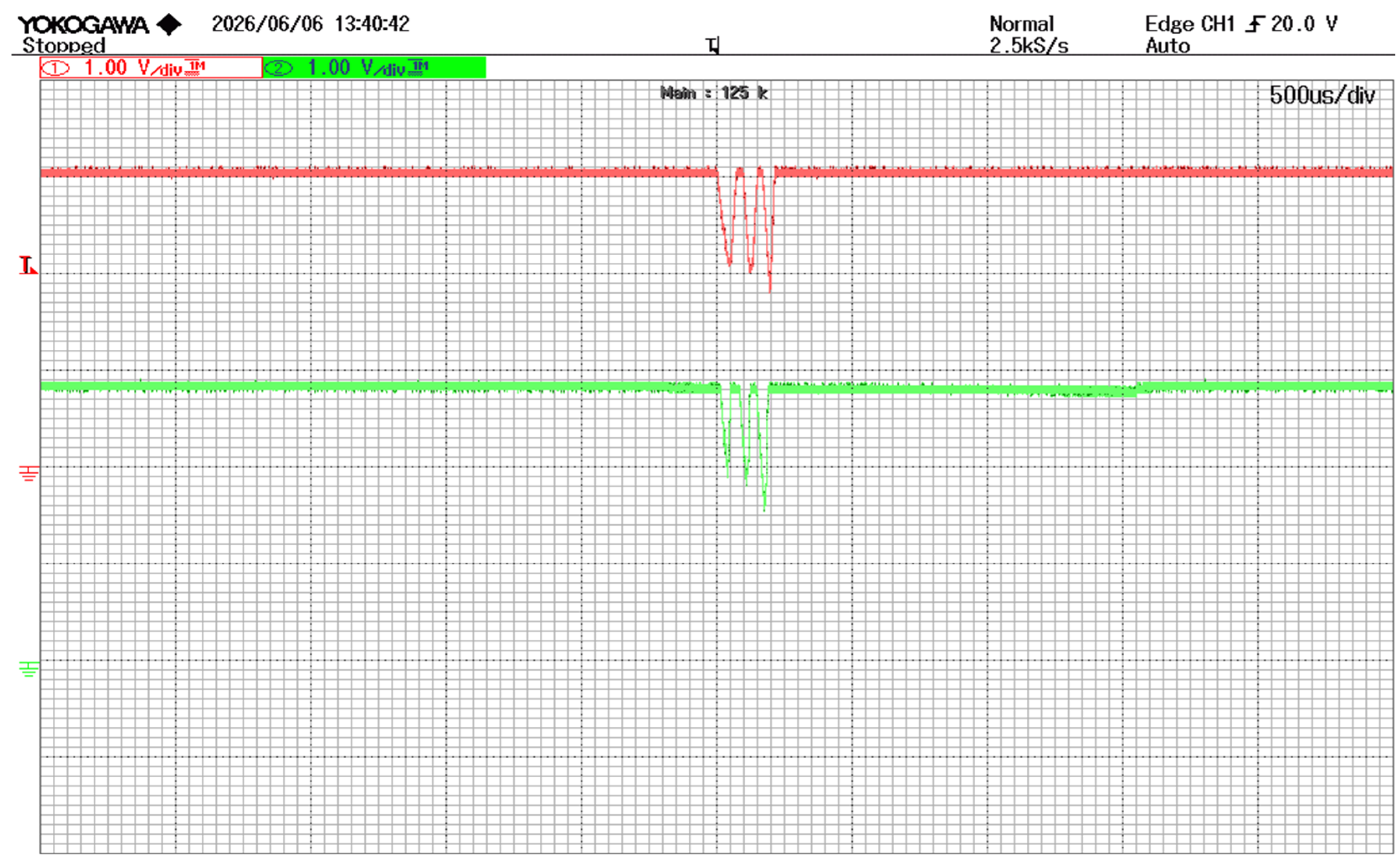
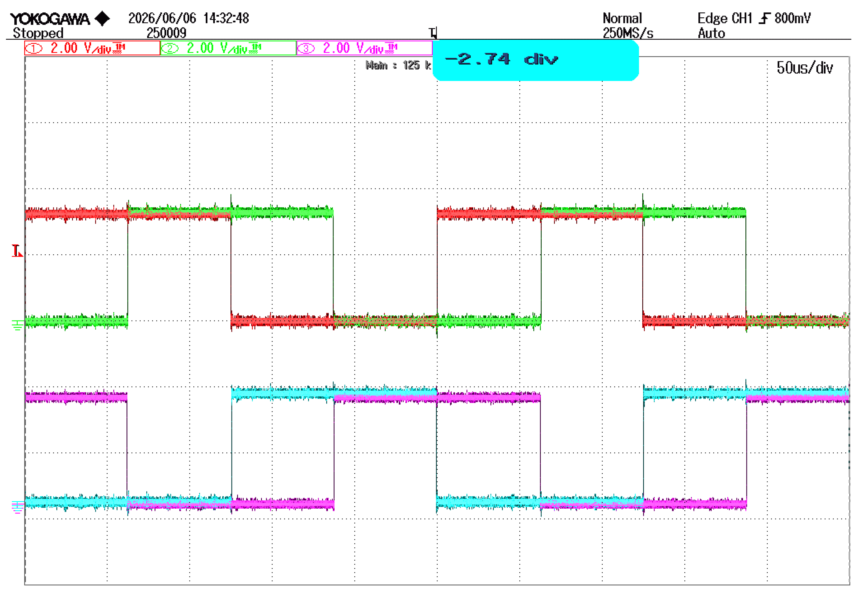
Figure 17 presents the steady-state voltage and current at load terminals during series-mode operation. A 60 V voltage and 0.78 A current are observed at load terminals. Figure 18 presents the transient condition for mode switch from series operation to parallel operation. The output voltage falls to 30 V from 60 V while current raises to 1.56 A from 0.78 A as seen from Figure 18, which validates the seamless on-load mode switching. Also, a quick transient of two switching cycles validates the simulation observation for the same quantities. It also presents the steady operation at parallel mode. Figure 19 presents the mode switch from parallel operation to independent operation, depicting the momentary disturbance in individual module voltages for three switching cycles which correlates to the equivalent simulation observation. Figure 20 presents the gating pulses during mode switch validating closed-loop current regulation. The steady-state transformer voltages are also presented in Figure 21 to validate DAB operation.

5. Performance Comparison and Merits of Proposed Converter

5.1. On-Load Configuration and Range Extension

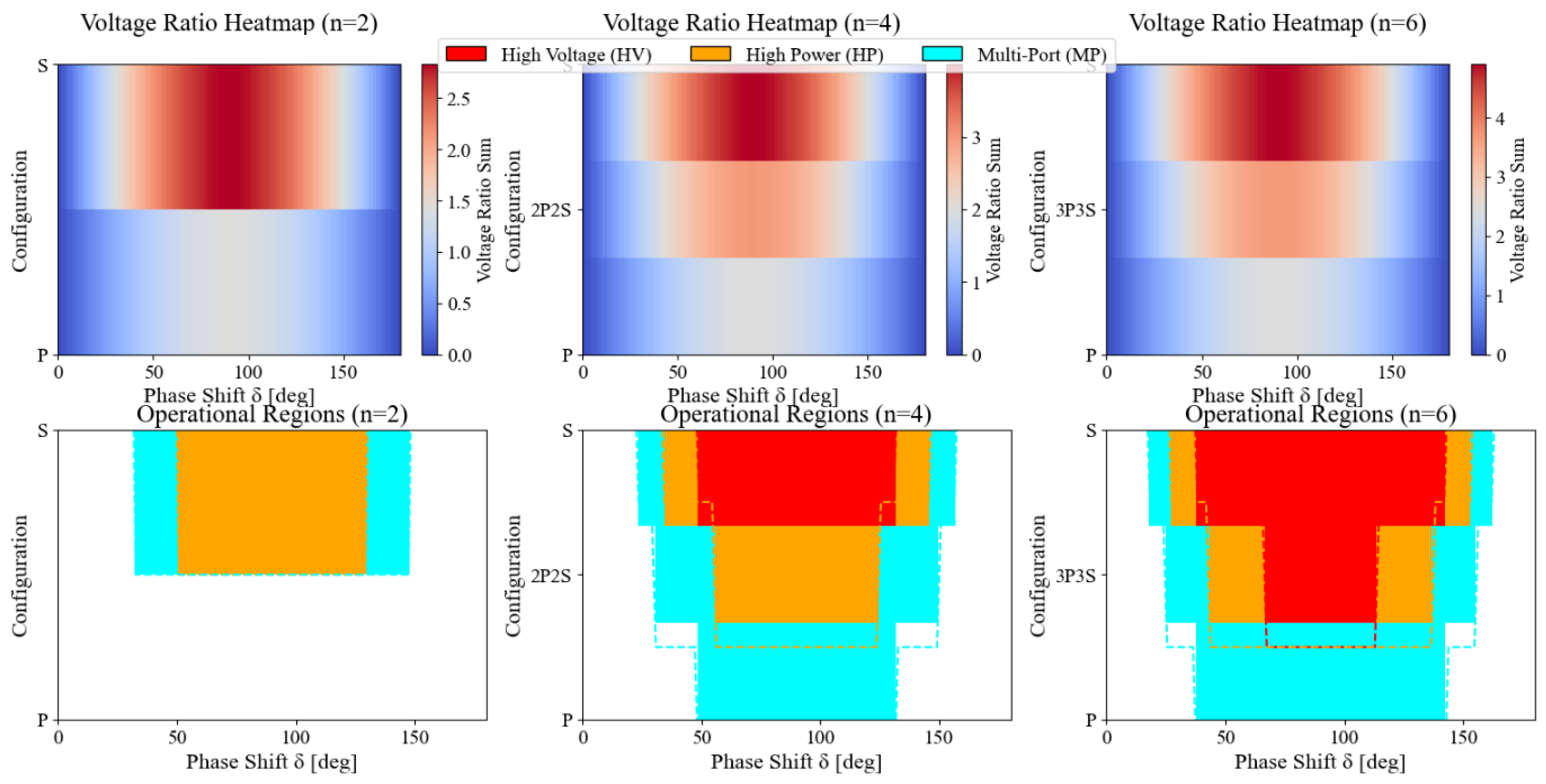
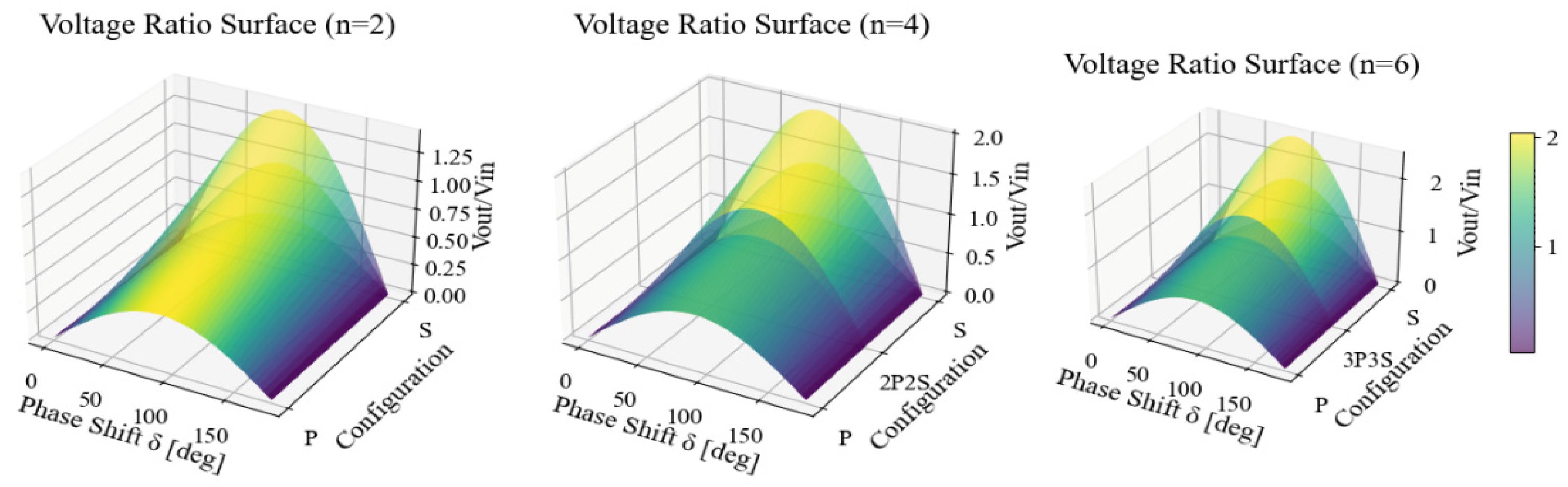
With the operational feasibility, configuration programming, and closed-loop control validated for implementation of the proposed converter, this section presents the merits of the converter in terms of wide-range voltage and power capabilities along with multi-port operation. The merits of the proposed converter are presented through deliverable voltages, powers, and multiple loads for various module sizes. Figure 22 presents the 3D surface of voltage gain against operational DAB phase shift for different combinations for DAB module numbers such as all parallel, series–parallel with increase in series modules, and all parallel for module sizes (n) of 2, 4 and 6. It is observed that gain up to 1.5 is feasible for n = 2. Also, with an increase in the number of DAB modules the voltage gain is increased to 1.75 for n = 4 and 2.5 for n = 6. Therefore, a large voltage range is delivered to the proposed converter. The higher voltages are delivered with increasing series combinations of PCMs at load side. The inclination in the surfaces of voltage gain towards series configurations of PCMs demonstrate this idea. However, with parallel combination of PCMs at load side, higher currents are delivered. Similar gains can be achieved with an existing converter with a larger number of modules, such as with n = 4 in [12] in comparison to n = 2 with the proposed converter.
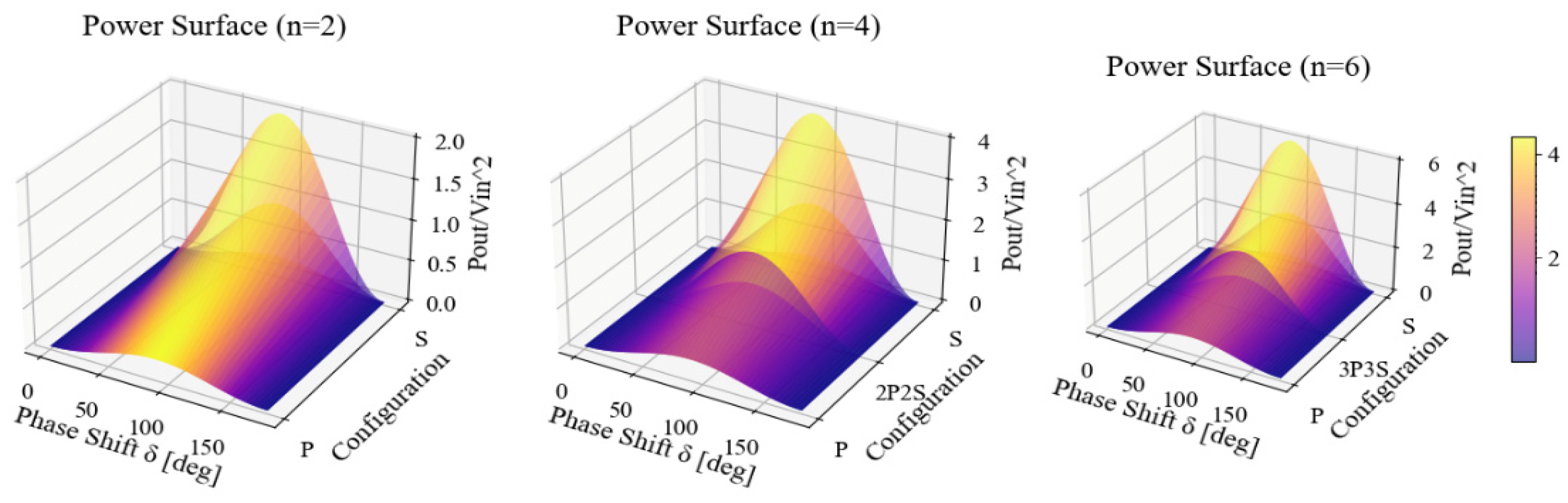
For similar module sizes, operational phase shift is considered for voltage gain; the corresponding power in terms of per unit input power is presented in Figure 23. It is observed that a wide range of power is supplied with a larger number of modules. The existing converters rely on voltage gain [13] or power delivery [14] in control, but the proposed controller ensures that both the parameters are controlled simultaneously with outer voltage and inner current loop control.
The multi-output capabilities of the converter are demonstrated in Figure 24 with the possible voltage ratios, along with boundaries separating high voltage, high power and multiple output regions. The series combinations provide HV and high-power operations, while parallel combinations or isolated combinations provide multiple output operations. In comparison to the multi-output configuration as in [15], it is validated that the proposed converter provides a wide range of options in the selection of multiple load operation.

5.2. Performance Comparison to Existing Power Converters

The per-module power is partitioned in the proposed converter so that required δ per module is in a feasible range to implement active phase shifting, while the existing multi-winding single-core designs [13,14] are implemented in the tens to a few hundreds of volts per port and power from 100 W to several kW per combined converter. Further, in terms of power handling and modular scaling, multi-winding designs [15,16] show kW ranges by combining multiple legs or modules, and Grinó’s modeling examples [17] include port-injected powers in the hundreds to thousands of watts in their simulations, which can effectively be achieved with the proposed converter with fewer modules as compared to stated approaches in [18,19]. The multi-port capability from the literature demonstrates both fixed multi-winding single-core converters and multi-core modular DAB arrays [24,25,26], but runtime reconfigurable series/parallel switching feature of the proposed converter is novel. Practically, to support runtime reconfiguration between series and parallel, it needs fast and low-loss disconnect switches. The significant operational performance parameters are compared to existing converters are presented in Table 5 to justify the potential for scalability through proposed conversion with programmable configuration and stringent closed-loop control of the proposed converter. The comparisons are made in terms of output voltage range, power delivery, phase shift range, output voltage ripple, output current ripple, and multiple output possibilities. These comparisons highlight the technical merits and potential applicability of the proposed converter for wide-range DC-DC conversion.
Although the proposed converter requires additional CM switches compared to manually configured configurations as observed from Table 5, these devices operate mainly during mode reconfiguration and therefore experience significantly lower switching activity than the main power switches. Nevertheless, the increased component count introduces additional conduction losses, which reduce overall efficiency. Detailed efficiency and reliability analyses are reserved for future work. Also, though the proposed topology demonstrates satisfactory performance under simulation and experimental validation, practical implementation at higher voltage and power levels may require additional consideration of parasitic effects, dead-time optimization, EMI mitigation, insulation requirements, and switching losses. Investigation of these aspects for large-scale deployment is reserved for future work.

6. Conclusions

Thus, the on-load configurable multi-module DAB is successfully implemented for voltage/current multiplication modes and multiple load mode. Simulation and experimental results justify feasible closed-loop regulation with the output voltages and currents regulated to required values at load ports. The transient settling time of 2–3 switching cycles verify the stringent on-load reconfiguration of converter. The developed converter exhibits favorable performance for power electronic applications involving varying voltage conversion ratios within the investigated operating range. Thus, the proposed converter provides a promising solution for applications requiring flexible voltage adaptation.

Author Contributions

Conceptualization, C.B.G., P.S.V. and C.R.R.; methodology, C.B.G. and E.S.P.; software, J.H.C.; validation, C.B.G., P.S.V., M.K.K., K.V.G.R., J.H.C., E.S.P. and C.R.R.; formal analysis, K.V.G.R.; investigation, C.B.G.; resources, K.V.G.R.; data curation, P.S.V.; writing—original draft preparation, C.B.G. and C.R.R.; writing—review and editing, J.H.C.; visualization, C.R.R.; supervision, C.R.R.; project administration, J.H.C.; funding acquisition, J.H.C. All authors have read and agreed to the published version of the manuscript.

Funding

This research received no external funding.

Institutional Review Board Statement

Not Applicable.

Informed Consent Statement

Not Applicable.

Data Availability Statement

The data presented in this study are available within the article. Additional simulation and experimental data supporting the findings of this work are available from the corresponding author upon reasonable request.

Conflicts of Interest

The authors declare no conflicts of interest.

References

  1. Ibanez, F.M.; Echeverria, J.M.; Vadillo, J.; Fontan, L. A step-up bidirectional series resonant DC/DC converter using a continuous current mode. IEEE Trans. Power Electron. 2015, 30, 1393–1402. [Google Scholar] [CrossRef]
  2. Malan, W.; Vilathgamuwa, D.M.; Walker, G. Modeling and control of a resonant dual active bridge with a tuned CLLC network 1-1. IEEE Trans. Power Electron. 2015, 31, 7297–7310. [Google Scholar] [CrossRef]
  3. Twiname, R.P.; Thrimawithana, D.J.; Madawala, U.K.; Baguley, C.A. A dual-active bridge topology with a tuned CLC network. IEEE Trans. Power Electron. 2015, 30, 6543–6550. [Google Scholar] [CrossRef]
  4. Kim, H.-S.; Ryu, M.-H.; Baek, J.-W.; Jung, J.-H. High-efficiency isolated bidirectional AC–DC converter for a DC distribution system. IEEE Trans. Power Electron. 2013, 28, 1642–1654. [Google Scholar] [CrossRef]
  5. He, J.; Chen, Y.; Lin, J.; Chen, J.; Cheng, L.; Wang, Y. Review of Modeling, Modulation, and Control Strategies for the Dual-Active-Bridge DC/DC Converter. Energies 2023, 16, 6646. [Google Scholar] [CrossRef]
  6. Koohi, P.; Watson, A.J.; Clare, J.C.; Soeiro, T.B.; Wheeler, P.W. A Survey on Multi-Active Bridge DC-DC Converters: Power Flow Decoupling Techniques, Applications, and Challenges. Energies 2023, 16, 5927. [Google Scholar] [CrossRef]
  7. Chen, L.; Lin, L.; Shao, S.; Gao, F.; Wang, Z.; Wheeler, P.W.; Dragičević, T. Moving Discretized Control Set Model-Predictive Control for Dual-Active-Bridge with the Triple-Phase Shift. IEEE Trans. Power Electron. 2020, 35, 8624–8637. [Google Scholar] [CrossRef]
  8. Tarisciotti, L.; Chen, L.; Shuai, S.; Dragičević, T.; Wheeler, P.W.; Zanchetta, P. Finite Control Set Model Predictive Control for Dual Active Bridge Converter. IEEE Trans. Ind. Appl. 2022, 58, 2155–2165. [Google Scholar] [CrossRef]
  9. Bai, H.; Mi, C.C. The Short-Time-Scale Transient Processes in High-Voltage and High-Power Isolated Bidirectional DC-DC Converters. IEEE Trans. Power Electron. 2008, 23, 2648–2656. [Google Scholar] [CrossRef]
  10. Zhao, B.; Song, Q.; Liu, W.; Liu, G.; Zhao, Y. Universal high-frequency-link characterization and practical fundamental-optimal strategy for dual-active-bridge DC-DC converter under PWM plus phase-shift control. IEEE Trans. Power Electron. 2015, 30, 6488–6494. [Google Scholar] [CrossRef]
  11. Shao, S.; Jiang, M.; Ye, W.; Li, Y.; Zhang, J.; Sheng, K. Modeling and advanced control of dual-active-bridge DC-DC converters: A review. IEEE Trans. Power Electron. 2022, 37, 1524–1547. [Google Scholar] [CrossRef]
  12. Abdelaziz, Y.N.; Abdel-Moneim, M.G.; Aboushady, A.A.; Abdel-Khalik, A.S.; Hamad, M.S. A ring-connected dual active bridge based DC-DC multiport converter for EV fast-charging stations. IEEE Access 2022, 10, 52484–52499. [Google Scholar] [CrossRef]
  13. Harrison, S.; Soltoswski, B.; Pepiciello, A.; Farag, A.H.; Mebtu, M.B.; Xu, L.; Egea-Álvarez, A.; Cheah-Mañé, M.; Gomis-Bellmunt, O. Review of multiport power converters for distribution network applications. Renew. Sustain. Energy Rev. 2024, 203, 114742. [Google Scholar] [CrossRef]
  14. Farajdadian, S.; Hajizadeh, A. Recent developments of multiport DC/DC converter topologies, control strategies and applications: A comparative review and analysis. Energy Rep. 2024, 11, 1019–1045. [Google Scholar] [CrossRef]
  15. Nguyen, N.D. A model predictive voltage control for dual-active-bridge converters using the generalized averaging model. Int. J. Control Autom. Syst. 2023, 21, 2455–2463. [Google Scholar] [CrossRef]
  16. Kong, D.; Gao, X.; Zhang, Z.; Liu, C.; Heldwein, M.L.; Kennel, R. Minimization of current stress for dual active bridge converters based on model predictive control with enhanced ZVS ability. IEEE Trans. Ind. Electron. 2024, 71, 6900–6911. [Google Scholar] [CrossRef]
  17. Wu, Y.; Qin, Z.; Bauer, P.; Wang, X.; Duarte, J.L.; Ferreira, B. A 150-kW 99%-efficient all-silicon-carbide triple-active-bridge converter for solar-plus-storage systems. IEEE J. Emerg. Sel. Top. Power Electron. 2022, 10, 3496–3510. [Google Scholar] [CrossRef]
  18. Wang, Y.; Guan, Y.; Molinas, M.; Fosso, O.B.; Hu, W.; Zhang, Y. Open-circuit switching fault analysis and tolerant strategy for dual-active-bridge DC-DC converter considering parasitic parameters. IEEE Trans. Power Electron. 2022, 37, 15020–15036. [Google Scholar] [CrossRef]
  19. Purgat, P.; Bandyopadhyay, S.; Qin, Z.; Bauer, P. Zero-voltage-switching criteria of triple active bridge converter. IEEE Trans. Power Electron. 2021, 36, 5425–5439. [Google Scholar] [CrossRef]
  20. Lin, Z.; Xu, D.; Wang, H.; Jiang, J.; Wu, X. A three-port LCC resonant converter for the 380-V/48-V hybrid DC system. IEEE Trans. Power Electron. 2022, 37, 10864–10876. [Google Scholar] [CrossRef]
  21. Krismer, F.; Kolar, J.W. Closed-form solution for minimum conduction loss modulation of dual-active-bridge converters. IEEE Trans. Power Electron. 2012, 27, 174–188. [Google Scholar] [CrossRef]
  22. De Doncker, R.W.; Divan, D.M.; Kheraluwala, M.H. A three-phase soft-switched high-power-density DC/DC converter for high-power applications. In Proceedings of the IEEE Industry Applications Society Annual Meeting, Pittsburgh, PA, USA, 2–7 October 1988; pp. 796–805. [Google Scholar] [CrossRef]
  23. Van-Long, P.; Wada, K. Applications of triple active bridge converter for future grid and integrated energy systems. Energies 2020, 13, 1577. [Google Scholar] [CrossRef]
  24. ElMenshawy, M.; Massoud, A. Development of modular DC-DC converters for low-speed electric vehicles fast chargers. Alex. Eng. J. 2021, 60, 1067–1083. [Google Scholar] [CrossRef]
  25. Iyer, V.M.; Gulur, S.; Gohil, G.; Bhattacharya, S. Extreme fast charging station architecture for electric vehicles with partial power processing. In Proceedings of the IEEE Applied Power Electronics Conference and Exposition (APEC), San Antonio, TX, USA, 4–8 March 2018; pp. 659–665. [Google Scholar] [CrossRef]
  26. Nguyen, H.V.; To, D.; Lee, D. Onboard battery chargers for plug-in electric vehicles with dual functional circuit for low-voltage battery charging and active power decoupling. IEEE Access 2018, 6, 70212–70222. [Google Scholar] [CrossRef]
  27. Kougioulis, I.; Pal, A.; Wheeler, P.; Ahmed, M.R. An isolated multiport DC-DC converter for integrated electric vehicle on-board charger. IEEE J. Emerg. Sel. Top. Power Electron. 2023, 11, 4178–4198. [Google Scholar] [CrossRef]
Figure 1. General n-module single-core DAB-based wide voltage range and multi-port power converter topology.
Actuators 15 00354 g001
Figure 2. Small signal model of individual DAB.
Actuators 15 00354 g002
Figure 3. Small signal model of the converter for configurable multiple mode DC-DC converter.
Actuators 15 00354 g003
Figure 4. Equivalent voltage bus model for multi-port operation.
Actuators 15 00354 g004
Figure 5. (a) On-load configuration and control parameter programming scheme. (b) Switching sequence for CMs during online mode transition.
Actuators 15 00354 g005
Figure 6. Closed-loop current control of configurable modular DAB converter.
Actuators 15 00354 g006
Figure 7. Experimental setup for configurable modular DAB converter.
Actuators 15 00354 g007
Figure 8. Voltages and currents at outputs of converter modules.
Actuators 15 00354 g008
Figure 9. Steady-state output voltages and current during series-mode operation.
Actuators 15 00354 g009
Figure 10. Transients in output voltages and currents for mode switch from series to parallel operation.
Actuators 15 00354 g010
Figure 11. Steady-state output voltages and current during parallel-mode operation.
Actuators 15 00354 g011
Figure 12. Transients in output voltages and currents for mode switch from parallel to independent operation.
Actuators 15 00354 g012
Figure 13. Steady-state output voltages and current during independent load operation.
Actuators 15 00354 g013
Figure 14. Voltage and current delivered by DC source during all operating conditions.
Actuators 15 00354 g014
Figure 15. Steady-state cycles of AC voltages and current in transformer.
Actuators 15 00354 g015
Figure 16. Steady-state cycles of voltage and current in power switches.
Actuators 15 00354 g016
Figure 17. Experimental waveforms for steady-state output voltages and current during series-mode operation.
Actuators 15 00354 g017
Figure 18. Experimental waveforms for output voltage and current during transient condition from series to parallel mode switch and steady-state parallel operation.
Actuators 15 00354 g018
Figure 19. Experimental waveforms for output voltage and current during transient condition from parallel mode to independent mode switch and steady-state independent load operation.
Actuators 15 00354 g019
Figure 20. Experimental results for gating signal modulation during closed-loop current regulation.
Actuators 15 00354 g020
Figure 21. Experimental result for few cycles of steady-state transformer winding voltages.
Actuators 15 00354 g021
Figure 22. Voltages supplied with phase shift control against converter configuration for various module sizes.
Actuators 15 00354 g022
Figure 23. Power delivered with phase shift control against converter configuration for various module sizes.
Actuators 15 00354 g023
Figure 24. Operational regions for various module sizes.
Actuators 15 00354 g024
Table 1. Switching combinations for configuration module.
Connection to Adjacent ModulesSPSSPPSNSSNP
Isolated0000
Series1010
Parallel0101
Upper series–lower parallel1001
Lower series–upper parallel0110
Table 2. Wide voltage range power conversion features of proposed converter.
Source Voltage RangeHV Load
Voltage Range
LV Load Voltage RangeIsolated Loads
NumberVoltage Range
nVDC n 2 K V DC     n K VDC 1 K V DC     n 4 VDCn, n 2 , …, 2   1 K V DC ,   2 K V DC ,   ,   n 2 K VDC
3 n 4 VDC 3 n 8 K V DC     3 n 4 K VDC 1 K V DC     3 n 16 VDC 3 n 4 , 3 n 8 , …, 2   1 K V DC ,   2 K V DC ,   ,   3 n 8 K VDC
n 2 VDC n 4 K V DC     n 2 K VDC 1 K V DC     n 8 VDC n 2 , n 4 , …, 2   1 K V DC ,   2 K V DC ,   ,   n 4 K VDC
n 4 VDC n 8 K V DC     n 4 K VDC 1 K V DC     n 16 VDC n 4 , n 8 , …, 2   1 K V DC ,   2 K V DC ,   ,   n 8 K VDC
Table 3. Control parameter programming for desired converter configuration.
Control ParameterKPI|Ilref|KPIϕlKPIdgb
Single load k 4 β L l k f s K 2 k 4 L l k f s K 2 R + γ 1 β k k 4 L l k f s K 2 R + γ 1 β ( k ) k 4 L l k f s K 2 R + γ
Multiple output ports k 4 β L l k f s K 2 m k 4 L l k f s K 2 R + γ 1 β m k k 4 L l k f s K 2 R + γ 1 β m k k 4 L l k f s K 2 R + γ
Table 4. Simulation and experimentation parameters.
Component/ParameterSimulation
Number of DAB modules, n2
Resistive Loads400 Ω
DC Source600 V (60 V for experimentation)
DC link capacitances, CDCx100 μF
PCM Filter inductors Lx50 μH
PIϕl0.873, 12.57
PI|Iref|0.245, 5.45
PIgdb0.1225, 2.725
HF Transformer600 V/300 V, 0.1 H, 0.025Ω
Power SwitchesIGBT 1200 V, 10 A
Switching Frequency5 kHz
Experimental DC Voltage sensingLV-25P, 100 mv/V setting
Experimental AC Voltage sensingLV-25P, 200 mv/V setting
Experimental Current SensingLA-25P, 1000 mV/1 A setting
Table 5. Performance comparison to existing converters.
Parameter[16][17][18][24][25][26]Proposed
Voltage Conversion Range (V)80150600600400400600
Rated Power (W)200100100500500500500
Phase Shift Range (°)30–15030–15030–15060–12060–12080–12080–100
Transformer
Structure
SingleSingleSingleMultiple
Independent
Multiple
Independent
Multiple
Independent
Single core
multiple
winding
Multiple OutputsNoNoNoYesYesYesYes
Demonstrated On-Load ReconfigurationNoNoNoNoNoNoYes
Additional Switches per PCM---2224
Disclaimer/Publisher’s Note: The statements, opinions and data contained in all publications are solely those of the individual author(s) and contributor(s) and not of MDPI and/or the editor(s). MDPI and/or the editor(s) disclaim responsibility for any injury to people or property resulting from any ideas, methods, instructions or products referred to in the content.