
A 3-to-5 V Input, 80 Peak-to-Peak Voltage (Vpp) Output, 2.75% Total Harmonic Distortion Plus Noise (THD+N), 2.9 μF Load Piezoelectric Actuator Driver with Four-Switch Buck–Boost


Abstract
1. Introduction
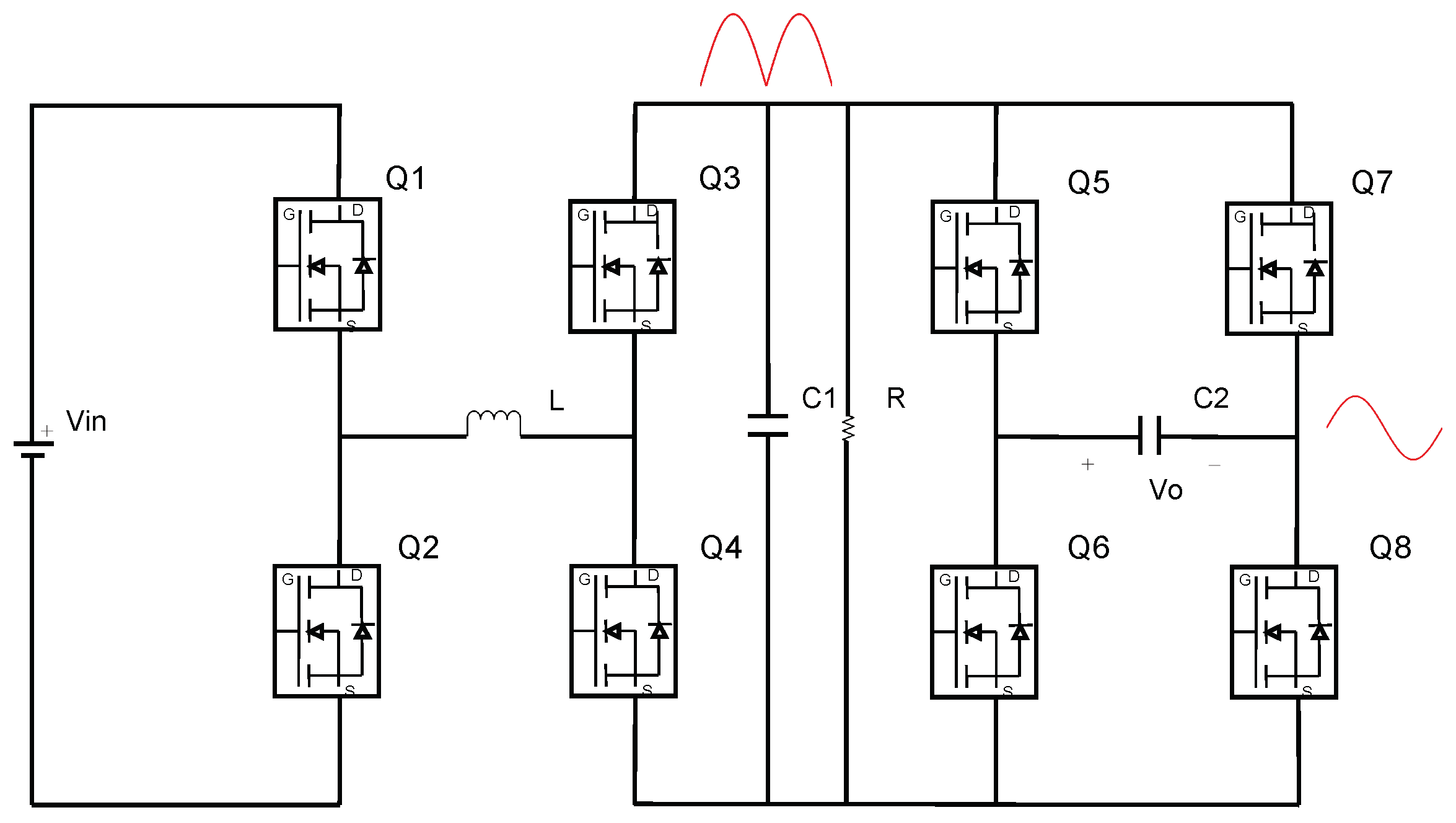
2. Proposed Method
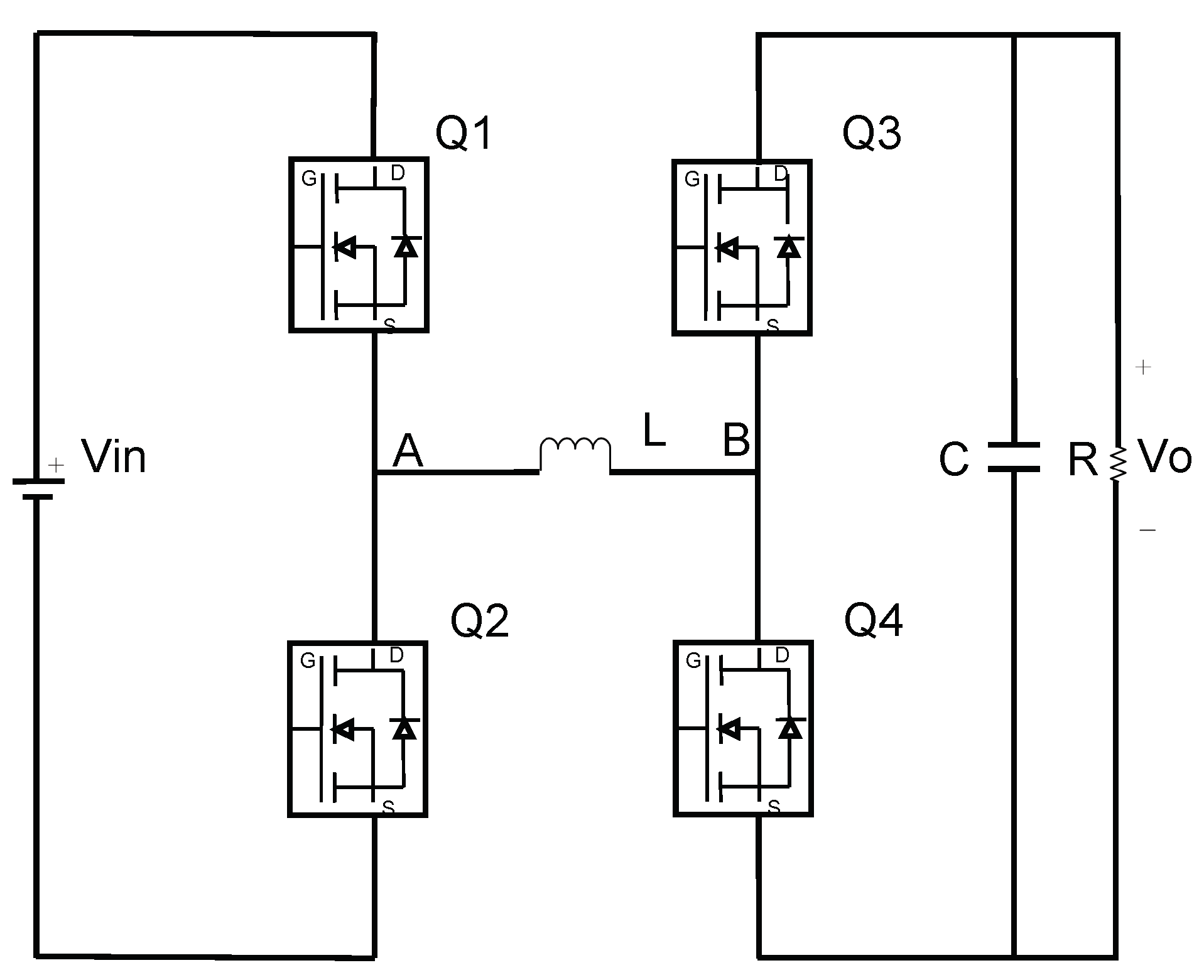
2.1. Four-Switch Buck–Boost Circuit
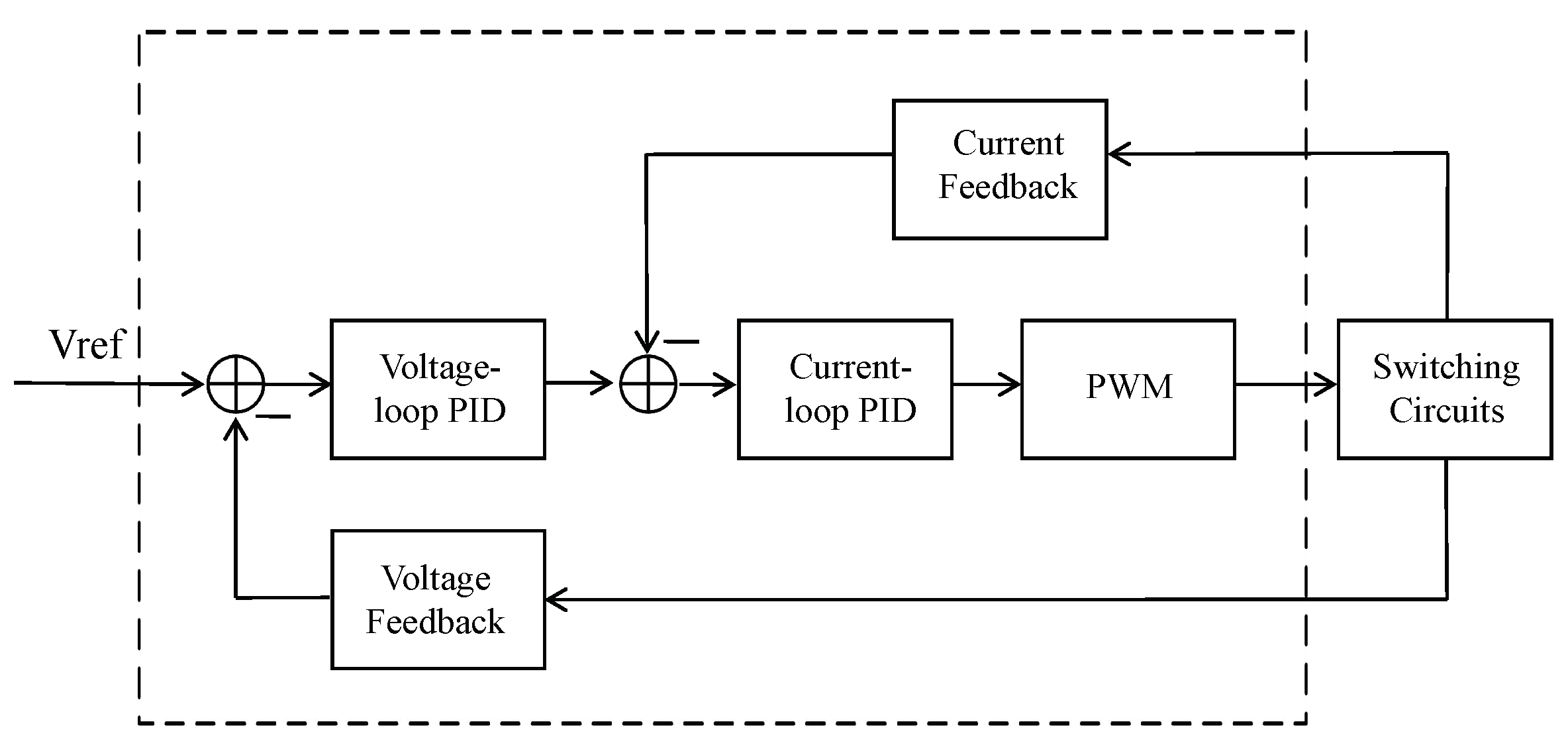
2.2. PI–P Feedback
3. Stability Analysis and Simulation
3.1. Root–Locus Diagram
3.2. Simulation
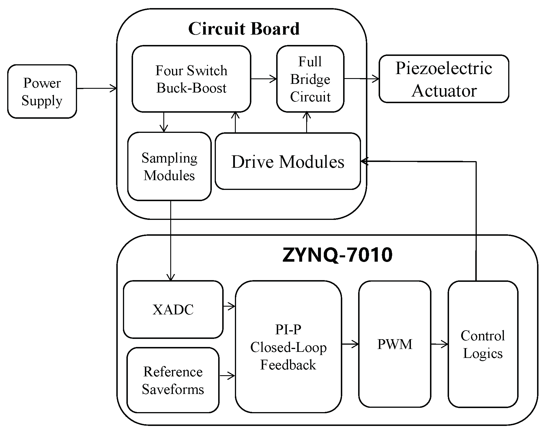
4. Implementation and Measured Comparison
4.1. System Implementation
4.2. Test Results and Comparison
5. Conclusions
Author Contributions
Funding
Data Availability Statement
Conflicts of Interest
References
- Wang, S.; Rong, W.; Wang, L.; Xie, H.; Sun, L.; Mills, J.K. A survey of piezoelectric actuators with long working stroke in recent years: Classifications, principles, connections, and distinctions. Mech. Syst. Signal Process. 2019, 123, 591–605. [Google Scholar]
- Delibas, B.; Koc, B.; Thielager, J.; Stiebel, C. A novel drive and control method for piezoelectric motors in microscopy stages. In Proceedings of the Euspen’s 21st International Conference & Exhibition, Copenhagen, Denmark, 12–19 June 2023; Volume 10. [Google Scholar]
- Jin, H.; Gao, X.; Ren, K.; Liu, J.; Qiao, L.; Liu, M.; Chen, W.; He, Y.; Dong, S.; Xu, Z.; et al. Review on piezoelectric actuators based on high-performance piezoelectric materials. IEEE Trans. Ultrason. Ferroelectr. Freq. Control 2022, 69, 3057–3069. [Google Scholar] [CrossRef] [PubMed]
- Lok, M.; Helbling, E.F.; Zhang, X.; Wood, R.; Brooks, D.; Wei, G.-Y. A Low Mass Power Electronics Unit to Drive Piezoelectric Actuators for Flying Microrobots. IEEE Trans. Power Electron. 2018, 33, 3180–3191. [Google Scholar] [CrossRef]
- Texas Instruments, DRV8662, Piezo Haptic Driver with Integrated Boost Converter. Available online: https://www.ti.com.cn/cn/lit/ds/slos740a/slos740a.pdf (accessed on 1 December 2014).
- Maxim Integrated, MAX77501, 110VPK-PKHigh-EffciencyPiezoHaptic. Available online: https://www.analog.com/media/en/technical-documentation/data-sheets/MAX77501.pdf (accessed on 1 May 2020).
- Reynolds, S. A High-Voltage, High-Frequency operational amplifier/Driver for Capacitive Loads. Meas. Sci. Technol. 1992, 3, 283–288. [Google Scholar] [CrossRef]
- Wallenhauer, C.; Gottlieb, B.; Zeichfusl, R.; Kappel, A. Efficiency-Improved High-Voltage Analog Power Amplifier for Driving Piezoelectric Actuators. IEEE Trans. Circuits Syst. Regul. Pap. 2010, 57, 291–298. [Google Scholar] [CrossRef]
- Pierco, R.; Torfs, G.; Verbrugghe, J.; Bakeroot, B.; Bauwelinck, J. A 16 Channel High-Voltage Driver with 14 Bit Resolution for Driving Piezoelectric Actuators. IEEE Trans. Circuits Syst. Regul. Pap. 2015, 62, 1726–1736. [Google Scholar] [CrossRef][Green Version]
- Rentmeister, J.S.; Kiani, M.H.; Pister, K.; Stauth, J.T. A 120–330V, Sub-μA, 4-Channel Driver for Microrobotic Actuators with Wireless-Optical Power Delivery and over 99% Current Efficiency. In Proceedings of the 2020 IEEE Symposium on VLSI Circuits, Honolulu, HI, USA, 16–19 June 2020; pp. 1–2. [Google Scholar]
- Huang, L.; Zhang, Z.; Andersen, M.A.E. A Review of High Voltage Drive Amplifiers for Capacitive Actuators. In Proceedings of the International Universities Power Engineering Conference (UPEC), London, UK, 4–7 September 2012. [Google Scholar]
- Chaput, S.; Brooks, D.; Wei, G.-Y. 21.5 A 3-to-5V input 100Vpp Output 57.7mW 0.42% THD+N Highly Integrated Piezoelectric Actuator Driver. In Proceedings of the IEEE International Solid-State Circuits Conference (ISSCC), San Francisco, CA, USA, 11–15 February 2017. [Google Scholar]
- Li, Y.; Dobbins, B.L.; Stauth, J.T. An 80-117V Pseudo-Adiabatic Drive Circuit for Microrobotic Actuators with Optical Power Delivery and Peak Power Reduction Factor over 14×. In Proceedings of the IEEE Custom Integrated Circuits Conference (CICC), Boston, MA, USA, 22–25 March 2020. [Google Scholar]
- Ren, X.; Ruan, X.; Qian, H. Three-mode dual-frequency two-edge modulation scheme for four-switch buck–boost converter. IEEE Trans. Power Electron. 2010, 24, 499–509. [Google Scholar]
- Leva, A. Autotuning of PI+p Controllers. In Proceedings of the IEEE International Conference on Computer-Aided Control Systems, Lyngby, Denmark, 31 July–2 August 1985. [Google Scholar]
- Ogata, K. Modern Control Engineering, 5th ed.; Prentice Hall: Upper Saddle River, NJ, USA, 2010; pp. 15–29. [Google Scholar]


| Boost | Buck–Boost | Four-Switch Buck–Boost | |
|---|---|---|---|
| Buck | no | yes | yes |
| Phase Shift of the Input and Output | same | reverse | same |
| Boost Capability (Vo/Vin) | |||
| MOS Voltage Stress | or |
| Voltage Outer Loop Proportionality Factor | Actual Voltage (Vpp) | THD |
|---|---|---|
| 0.25 | 190 | 1.75% |
| 0.5 | 198 | 0.96% |
| 1 | 196 | 0.74% |
| Voltage Outer Loop Integration Factor | Actual Voltage (Vpp) | THD |
|---|---|---|
| 100 | 198 | 0.96% |
| 150 | 197 | 1.06% |
| 300 | 198 | 1% |
| Current Inner Loop Proportionality Factor | Actual Voltage (Vpp) | THD |
|---|---|---|
| 8 | 198 | 0.96% |
| 12 | 194 | 1.02% |
| 16 | 192 | 1.21% |
| Ceramic Capacities (F) | Drive Voltage (Vpp) | Waveform Frequency (Hz) | THD | Actual Voltage (Vpp) |
|---|---|---|---|---|
| 0.1 | 200 | <=100 | 0.96% | 198 |
| 0.1 | 200 | <=200 | 1.74% | 197 |
| 0.2 | 180 | <=200 | 1.60% | 176 |
| 0.4 | 150 | <=150 | 2.00% | 148 |
| 0.8 | 150 | <=120 | 2.60% | 118 |
| 1 | 120 | <=200 | 2.70% | 118 |
| 2.2 | 120 | <=150 | 4.40% | 118 |
| 3.6 | 100 | <=150 | 3.24% | 99 |
| 4.4 | 100 | <=120 | 3.18% | 99 |
Disclaimer/Publisher’s Note: The statements, opinions and data contained in all publications are solely those of the individual author(s) and contributor(s) and not of MDPI and/or the editor(s). MDPI and/or the editor(s) disclaim responsibility for any injury to people or property resulting from any ideas, methods, instructions or products referred to in the content. |
© 2023 by the authors. Licensee MDPI, Basel, Switzerland. This article is an open access article distributed under the terms and conditions of the Creative Commons Attribution (CC BY) license (https://creativecommons.org/licenses/by/4.0/).
Share and Cite
Ye, R.; Chen, J.; Dong, S.; Li, B. A 3-to-5 V Input, 80 Peak-to-Peak Voltage (Vpp) Output, 2.75% Total Harmonic Distortion Plus Noise (THD+N), 2.9 μF Load Piezoelectric Actuator Driver with Four-Switch Buck–Boost. Actuators 2023, 12, 345. https://doi.org/10.3390/act12090345
Ye R, Chen J, Dong S, Li B. A 3-to-5 V Input, 80 Peak-to-Peak Voltage (Vpp) Output, 2.75% Total Harmonic Distortion Plus Noise (THD+N), 2.9 μF Load Piezoelectric Actuator Driver with Four-Switch Buck–Boost. Actuators. 2023; 12(9):345. https://doi.org/10.3390/act12090345
Chicago/Turabian StyleYe, Rui, Junbiao Chen, Shuxiang Dong, and Bing Li. 2023. "A 3-to-5 V Input, 80 Peak-to-Peak Voltage (Vpp) Output, 2.75% Total Harmonic Distortion Plus Noise (THD+N), 2.9 μF Load Piezoelectric Actuator Driver with Four-Switch Buck–Boost" Actuators 12, no. 9: 345. https://doi.org/10.3390/act12090345
APA StyleYe, R., Chen, J., Dong, S., & Li, B. (2023). A 3-to-5 V Input, 80 Peak-to-Peak Voltage (Vpp) Output, 2.75% Total Harmonic Distortion Plus Noise (THD+N), 2.9 μF Load Piezoelectric Actuator Driver with Four-Switch Buck–Boost. Actuators, 12(9), 345. https://doi.org/10.3390/act12090345