A Study on the Effect of Ambient Air Plasma Treatment on the Properties of Methylammonium Lead Halide Perovskite Films


R&D Centre for Low-Cost Plasma and Nanotechnology Surface Modifications (CEPLANT), Department of Physical Electronics, Faculty of Science, Masaryk University, Kotlářská 267/2, 611 37 Brno, Czech Republic
*
Author to whom correspondence should be addressed.
Metals 2019, 9(9), 991; https://doi.org/10.3390/met9090991
Submission received: 7 August 2019
/
Revised: 4 September 2019
/
Accepted: 5 September 2019
/
Published: 7 September 2019
(This article belongs to the Special Issue Plasmas Processes Applied on Metals and Alloys)
Abstract
:Organic-inorganic halide perovskite materials are considered excellent active layers in the fabrication of highly efficient and low-cost photovoltaic devices. This contribution demonstrates that rapid and low-temperature air-plasma treatment of mixed organic-inorganic halide perovskite film is a promising technique, controlling its opto-electrical surface properties by changing the ratio of organic-to-inorganic components. Plasma treatment of perovskite films was performed with high power-density (25 kW/m2 and 100 W/cm3) diffuse coplanar surface barrier discharge (DCSBD) at 70 °C in ambient air. The results show that short plasma treatment time (1 s, 2 s, and 5 s) led to a relatively enlargement of grain size, however, longer plasma treatment time (10 s and 20 s) led to an etching of the surface. The band-gap energy of the perovskite films was related to the duration of plasma treatment; short periods (≤5 s) led to a widening of the band gap from ~1.66 to 1.73 eV, while longer exposure (>5 s) led to a narrowing of the band gap to approx. 1.63 eV and fast degradation of the film due to etching. Surface analysis demonstrated that the film became homogeneous, with highly oriented crystals, after short plasma treatment; however, prolonging the plasma treatment led to morphological disorders and partial etching of the surface. The plasma treatment approach presented herein addresses important challenges in current perovskite solar cells: tuning the optoelectronic properties and manufacturing homogeneous perovskite films.
1. Introduction
Organic-inorganic halide perovskites have recently attracted considerable attention, largely because of their outstanding opto-electronic qualities, among them a high absorption coefficient, tunable band-gap energy, and high charge-carrier mobility [1,2,3,4]. In recent years, the power conversion efficiency of perovskite solar cells (PSCs) has been improved from an initial 3% to over 25% through a variety of development technologies, including solvent engineering, chemical composition management, and the employment of different fabrication architecture within the cells [5,6]. One of the main challenges in the production of high-efficiency PSCs is the control of surface composition and morphology in such a way as to obtain perovskite films with smooth surfaces [7,8,9]. Organic-inorganic halide perovskite has been deposited and processed in many different ways, resulting in films of various surface compositions and morphology. For example, the average grain size of deposited perovskite films has been reported as varying from nanoscale to microscale [10]. The surface composition and morphology of a perovskite layer strongly influence its energy-level alignment, exciton diffusion length, mobility, lifetime, and generally affecting performance of the PSCs. Much effort has, therefore, been devoted to controlling the surface composition and morphology of perovskite films [11,12,13,14]. Recently, post-processing methods have been developed to improve their surface properties [15]. Thermal annealing of deposited perovskite films is one of the common processes that influence the quality of the film [16]. Surface passivation engineering has been demonstrated as having a remarkable effect on efficiency enhancement of the PSCs by the amelioration of defects and optimization of grain boundaries at the surface. In addition, surface properties of the other layers such as TiO2 and PEDOT:PSS could significantly affect the performance of PCSs. For instance, Masood et al. studied the effect of TiO2 thickness on the performance of PSCs [17]. Zhang et al. showed that treatment of the PEDOT:PSS buffer layer could enhance the efficiency of PSCs [18].
A wide range of procedures related to the post-treatment of perovskite films have been undertaken recently in the quest to produce high-quality perovskite and enhance the performance of PSCs. Microwave irradiation has proved a rapid and controllable post-treatment means of improving efficiency of the PSCs through the enhancement of crystallization [19]. Ren et al. reported on perovskite films annealed in an oxygen atmosphere for 12 h at various temperatures from room temperature to 85 °C [20]. Yang et al. reported that a time-temperature-dependent post-treatment (post-annealing) of a CH3NH3PbIxCl3−x film led to a homogenous and highly oriented crystalline perovskite film that improved performance [21]. Plasma treatment has also shown great promise for surface treatment of perovskite films. Xiao et al. reported that low-pressure RF argon plasma treatment of the perovskite active layer can significantly improve the efficiency of PSCs [22]. The argon plasma treatment enhanced charge collection at the interface between the perovskite and electrode by altering the organic-to-inorganic ratio at the surface of perovskite layer. Plasma may also be employed for surface treatment of a wide range of materials. For example, UV/ozone plasma improves the optical and electrical characteristics of hybrid polymer-metal (PEN-Ag) electrodes in polymer solar cells [23]. CO2 plasma treatment significantly heightens surface wettability, and thereby the electrical conductivity of TiO2 transparent electrodes, improving the performance of the final device [24]. Ambient air plasma activation of the mesoscopic TiO2 layer affects the efficiency of the PSC [25].
In the investigation presented herein, mixed organic-inorganic halide perovskite (CH3NH3PbIxCl3−x) films were deposited on quartz glass and then treated with low-temperature ambient-air surface plasma. The plasma was generated by diffuse coplanar surface dielectric barrier discharge (DCSBD), details of which appear in Černák et al. [26]. DCSBD ambient-air plasma has recently been tested for rapid and low-temperature calcination of TiO2, Al2O3, and CeO2 nanofibers [27,28,29,30], mineralization of TiO2 mesoporous flexible photoanodes [31,32], and arrangement within an enclosed system with hydrogen gas to allow swift production of flexible reduced graphene oxide electrodes on PET foils [33]. Here, CH3NH3PbIxCl3−x perovskite films were spin-coated on to quartz glass and the effects of plasma treatment on the morphological and optoelectronic properties of these films were investigated. The results showed that, plasma treatment effectively removed organic methylammonium cations (CH3NH3 or MA) from the surface, however prolonging the plasma treatment lead to partially etching the surface. The work demonstrates that optoelectronic qualities of perovskite films, as measured by UV–VIS and ultraviolet photoelectron spectroscopy, can respond significantly to the surface composition and morphology. The chemical composition of the mixed halide perovskite films was evaluated by X-ray photoelectron spectroscopy (XPS) and Fourier transform infrared spectroscopy attenuated total reflectance (ATR-FTIR). Short plasma treatment (≤5 s) led to homogeneous perovskite films of larger grain size, as detected by X-ray diffraction (XRD) and scanning electron microscopy (SEM).
2. Experimental Section
2.1. Film Deposition
Perovskite precursor ink (a mixture of methylammonium iodide (MAI) and lead chloride (PbCl) dissolved in dimethyl formamide) was purchased from Ossila, UK. Prior to deposition, the perovskite solution was heated to 70 °C for 2 h. A quartz glass sheet was cut into small pieces (1 cm × 1 cm), then ultrasonically cleaned for 6 min in acetone, followed by isopropyl alcohol and deionized water. The samples were pre-treated with air plasma for 16 s (the optimum pre-treatment time for obtaining a uniform film on the substrate). After plasma pre-treatment, the samples were placed in a spin coater and perovskite ink was deposited on the substrate at a speed of 3000 rpm; the volume of the perovskite ink on each sample was 10 µL. All samples were then placed on a hotplate set at a temperature of 80 °C for 2 h. All the processes of the sample and ink deposition are performed in ambient-air conditions ranging from 20 °C to 24 °C and at a relative humidity of ≤35%.
2.2. Plasma Processing
Ambient-air plasma was generated by dielectric barrier discharge with a coplanar configuration of the electrodes using a diffuse coplanar surface barrier discharge (DCSBD) unit manufactured by Roplass s.r.o. (Brno, Czech Republic). The power density of plasma was maintained at 25 kW/m2 and 100 W/cm3. The deposited films were exposed to plasma for various treatment times ranging from 1 s to 20 s. Further, the deposited samples were treated at a range of distances between sample and plasma (from 0.1 to 0.7 mm). A distance of 0.6 mm was selected for the experiment because this was considered the optimal distance in light of the results (Figure S1, supplementary materials).
2.3. Characterization
A PerkinElmer Lambda 1050 UV–VIS spectrometer (Akron, OH, USA) was employed to measure the optical properties of the perovskite films at wavelengths from 380 nm to 800 nm. X-ray diffraction studies (XRD) were conducted using a Rigaku Smartlab (The Woodlands, TX, USA), with CuKα (λ = 1.54059A°) radiation. Ultraviolet photoelectron spectroscopy (UPS) was performed by Kratos Supra (Wharfside, Manchester, UK) under normal emission using He I (21.22 eV). The spectra were calibrated at the Fermi edge, which is the energy of the fastest emitted electron. To separate the secondary electron (SE) onset of the samples from that of the detector, a negative bias was applied to the samples. Chemical analysis of the samples was carried out by X-ray photoelectron spectroscopy (XPS) using an ESCALAB 250Xi of Al Kα X-ray source (Thermo Fisher Scientific, Loughborough, UK). The XPS spectra were acquired from two spots (650 µm) with a take-off angle of 90° in 10−8 mbar vacuum at 20 °C. Additional chemical information from the samples was obtained by using attenuated total reflectance Fourier transform infrared (ATR-FTIR) with a Bruker Vertex 80 V spectrometer (Brno, Czech Republic). The perovskite films were measured in attenuation total reflection (ATR) mode using a diamond crystal at a pressure of 2.51 hPa, spectral range from 4000 to 600 cm−1 and a resolution of 4 cm−1. A MIRA3 scanning electron microscope (Tescan, Czech Republic) was used to evaluate the morphology of the perovskite films before and after plasma treatment. To minimize the influence of environment on the plasma-treated perovskite films, the time between plasma treatment and surface characterization was always less than 1 h and samples were transported under nitrogen atmosphere with neither oxygen nor moisture.
3. Results and Discussion
XRD patterns for perovskite films before and after plasma treatment appear in Figure 1a. The peak located at 14.1° corresponding to the (110) plane belongs to the MAPbI3−xClx phase and the intensity of this peak decreased after plasma treatment but each treatment time led to different intensity. A notable diffraction peak at 15.5° corresponding to the (001) plane of the perovskite film appeared after a short plasma treatment time (1 s), indicating the formation of a MAPbCl3 perovskite structure. Prolonging the plasma treatment time led to increases in the intensity of this peak. Another peak of MAPbCl3 located at 16.5° corresponding to the (012) plane appeared after the plasma treatment. The peaks located at 28.5°, 29.3°, and 31.8° correspond to the (220), (002), and (310) planes of MAPbI3, respectively. The peak of (310) shifted to a lower angle after plasma treatment, a change perhaps related to an expanded crystal lattice. The intensity of the peak at 28.5° increased after plasma treatment which could be related to the enhancement of crystallinity within the perovskite film [34].
A slight diffraction of the PbI2 peaks at the (100) plane appeared in the XRD pattern. Figure 1b shows the location of some perovskite planes in the unit cell. The presence of the PbI2 peaks on the “untreated” sample refers to the incomplete conversion to the perovskite phase, and the peak shifted to a lower angle after plasma treatment. The PbI2 peaks detected on the plasma-treated films could be attributed to partial decomposition of the film. According to the Dubey et al. [35], the decomposition of perovskite film originates from moisture in the air. In addition, PbI2 peak showed different trends after plasma treatment: short plasma treatment (≤5 s) led to a decrease of the PbI2 intensity and prolonging the plasma treatment increased the intensity of PbI2. Furthermore, the calculated sizes of the PbI2 crystallite using the Scherrer equation (Figure S2) showed the same trend of the PbI2 peak before and after plasma treatment.
Figure 2 shows the UV–VIS absorption spectra of the perovskite film before and after plasma treatment. These demonstrate that plasma treatment led to shifts in the spectra of the perovskite film, varying with treatment times. A blue-shift of the absorption band edge occurred after short plasma treatment (≤5 s). The absorption band edge of the “untreated” perovskite film, the starting location at approx. 743 nm, shifted to approx. 713–716 nm after short plasma treatments (1 s and 2 s). The band edge after 5 s appeared at approx. 718 nm. Prolonging the treatment moved the band edge towards surprisingly higher wavelengths (red-shift), whereas 10 s of plasma treatment shifted the absorption band edge to approx. 757 nm. After 20 s of treatment, the band edge lay at a wavelength of 760 nm.
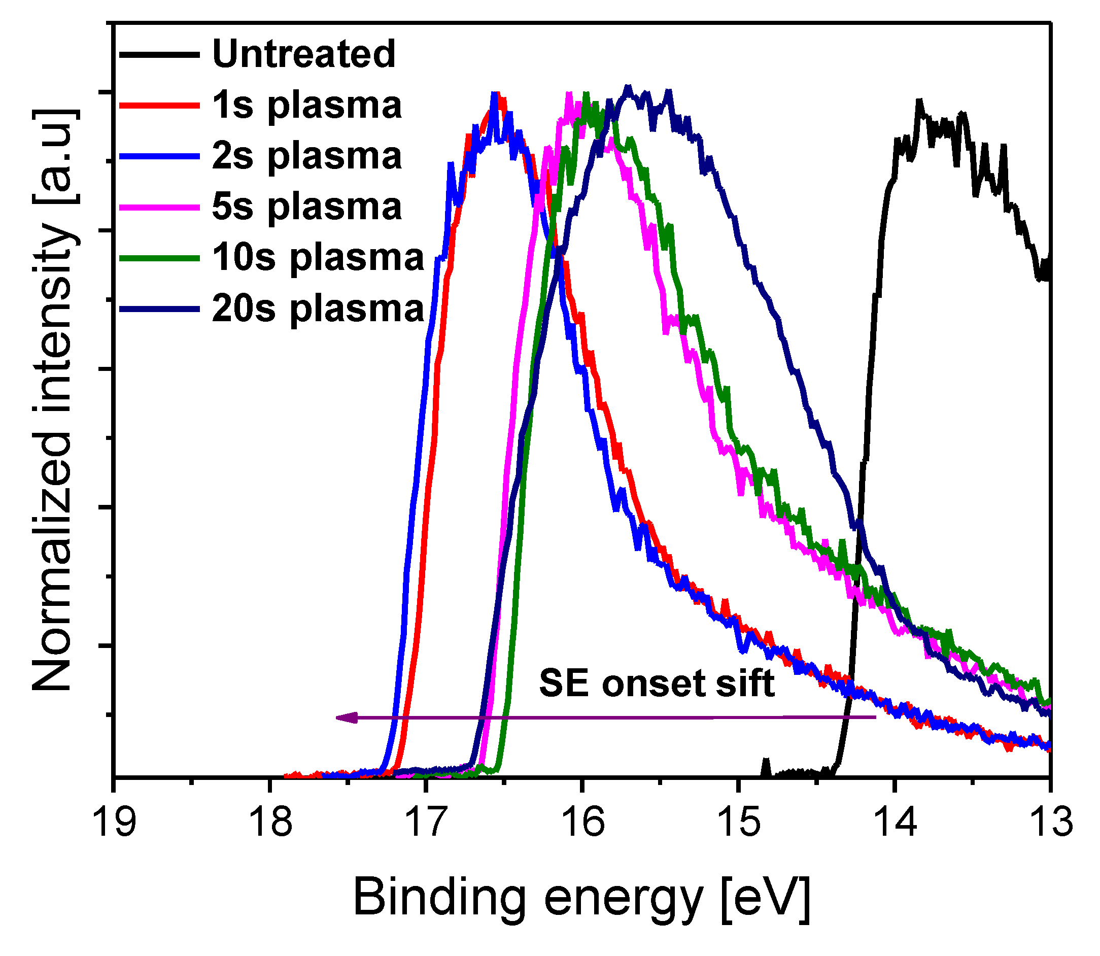
Secondary onset (SE onset) and valance bands of the perovskite films were measured by UPS; the results appear in Figure 3 and Figure S3, respectively.
The SE onset and valance band maximum (VBM) of the “untreated” perovskite films on quartz glass were located at 14.36 eV and 4.24 eV, respectively. The SE onset of the perovskite film shifted towards higher binding energy after plasma treatment and the maximum shift appeared after treatment for 2 s, with the SE onset located at a binding energy of 17.27 eV. Measurement of UPS indicated that the VBM of the perovskite films reacted differently to shorter and longer treatment times. Short plasma treatment shifted the valence bands to lower binding energy, with the VBM located at 2.39–2.46 eV after 1–5 s. In contrast, prolonged plasma treatment resulted in the VBM at higher binding energy, with the VBM located at 6.63 and 10.41 eV after plasma treatment for 10 s and 20 s, respectively.
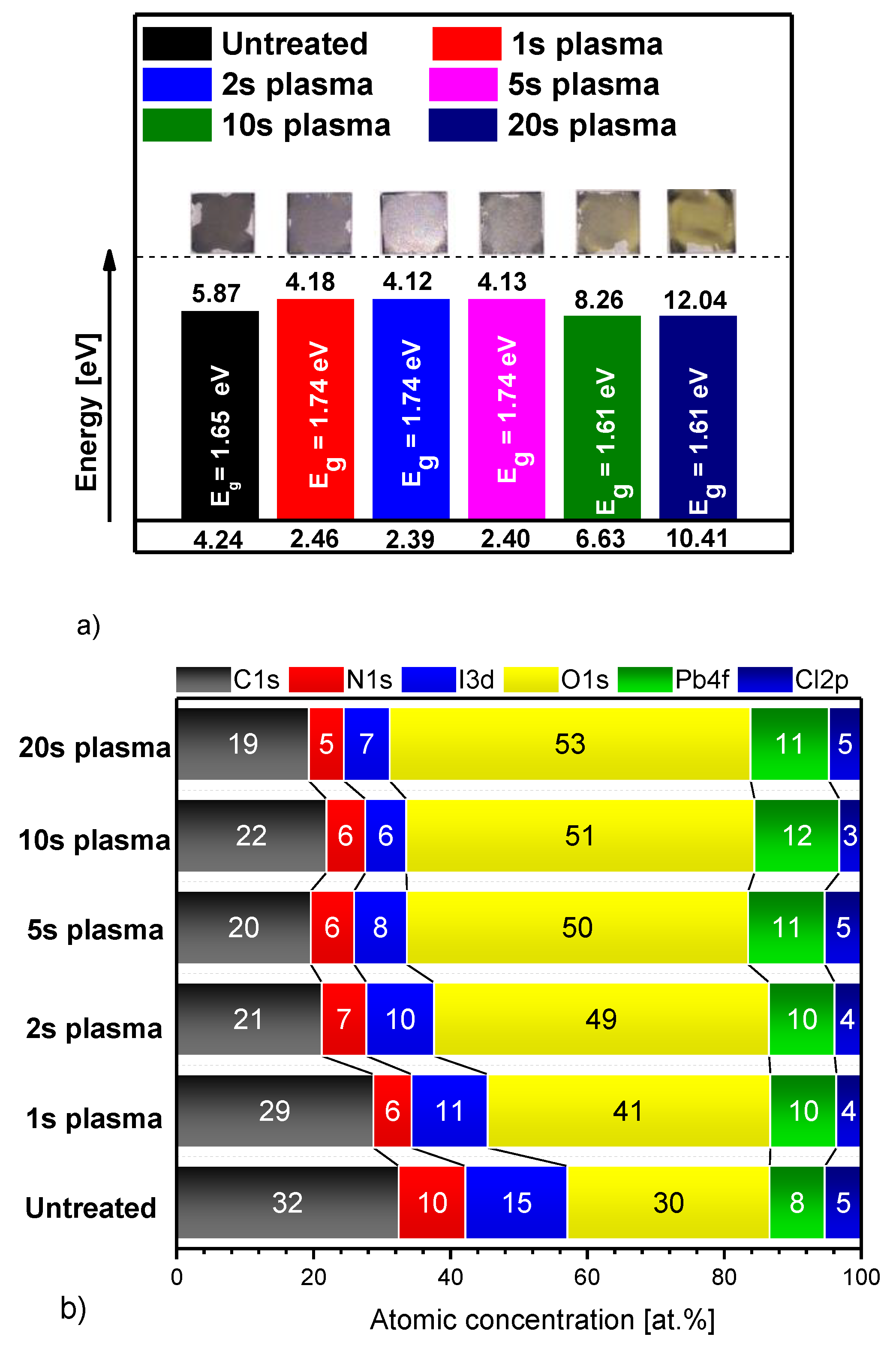
The conduction band edge, or minimum conduction band (mCB), of the perovskite film was estimated by means of band gap energy and maximum valance band. The band gap energy (Eg) can be calculated by using hc/λ, where ‘h’ is Plank’s constant, c is the speed of the light in vacuum, and λ is the wavelength corresponding to the band edge within the UV–VIS absorption spectra. Figure 4a shows the variation of the energy bands (including Eg, VBM, and mCB) of the perovskite films during plasma treatment, together with corresponding photographs taken after deposition. In general, the band gap shifts relate to changes in carrier concentration [36], meaning that a band gap shift toward larger values corresponds to a higher carrier concentration. The band gap widening after short plasma treatment (≤5 s) could, thus, be attributed to a higher concentration of charge carriers within the perovskite film. Further, the higher energy band was associated with decreases in VBM and mCB to lower energy levels. However, longer plasma treatment led to narrowing of the band gap of the mixed halide perovskite film, associated with higher energy levels of VBM and mCB.
It is well known that ambient air plasma treatment removes organic contamination from surfaces and induce oxygen-containing functional groups to the surface [37]. It was, therefore, anticipated that plasma treatment would lead to a decrease in the organic part of the mixed-halide perovskite film, e.g., in methylammonium cations (CH3NH3+). Evaluation of the chemical stoichiometry of the perovskite film before and after plasma treatment was performed by means of XPS measurement. Figure 4b summarizes the XPS results, including atomic concentration as a function of the plasma treatment time. The atomic concentration of the C1s peak decreased from approx. 32.4 at%, corresponding to the “untreated” perovskite film, to 28.7 at% after short plasma treatment (1 s). Plasma treatment for 2 s led to a concentration of the C1s peak to 21.2 at%, while prolonging the plasma treatment to 20 s led to a concentration of C1s of 19.3 at%. Longer plasma treatment times >5 s had no further effect on the composition of the perovskite surface probably due to homogeneous etching of the perovskite film, which is a different process than etching of the outermost layer of the surface. The XPS results disclosed that the lower concentration of C1s is accompanied by a dramatic decrease in the N1s and I3d concentrations after plasma treatment. In addition, the atomic concentration of oxygen was enhanced. High energy species of plasma could etch the surface of the perovskite film which broke the chemical bonds of the organic and halide components. The bonding of Pb is too strong for plasma to break it but contamination removal from the outermost layer of surface led to an increase in Pb concentration. The concentration of Pb4f increased from 8.1 to 9.7 at% after short plasma treatment (1 s). Prolonging the plasma treatment led to an increase in the Pb4f concentration. The rise in lead (Pb4f) concentration was related to the removal of organic contamination from the surface. Lead concentration remained constant after plasma treatment for 5 s, indicating that plasma penetration to the bulk of the mixed-halide perovskite films was negligible.
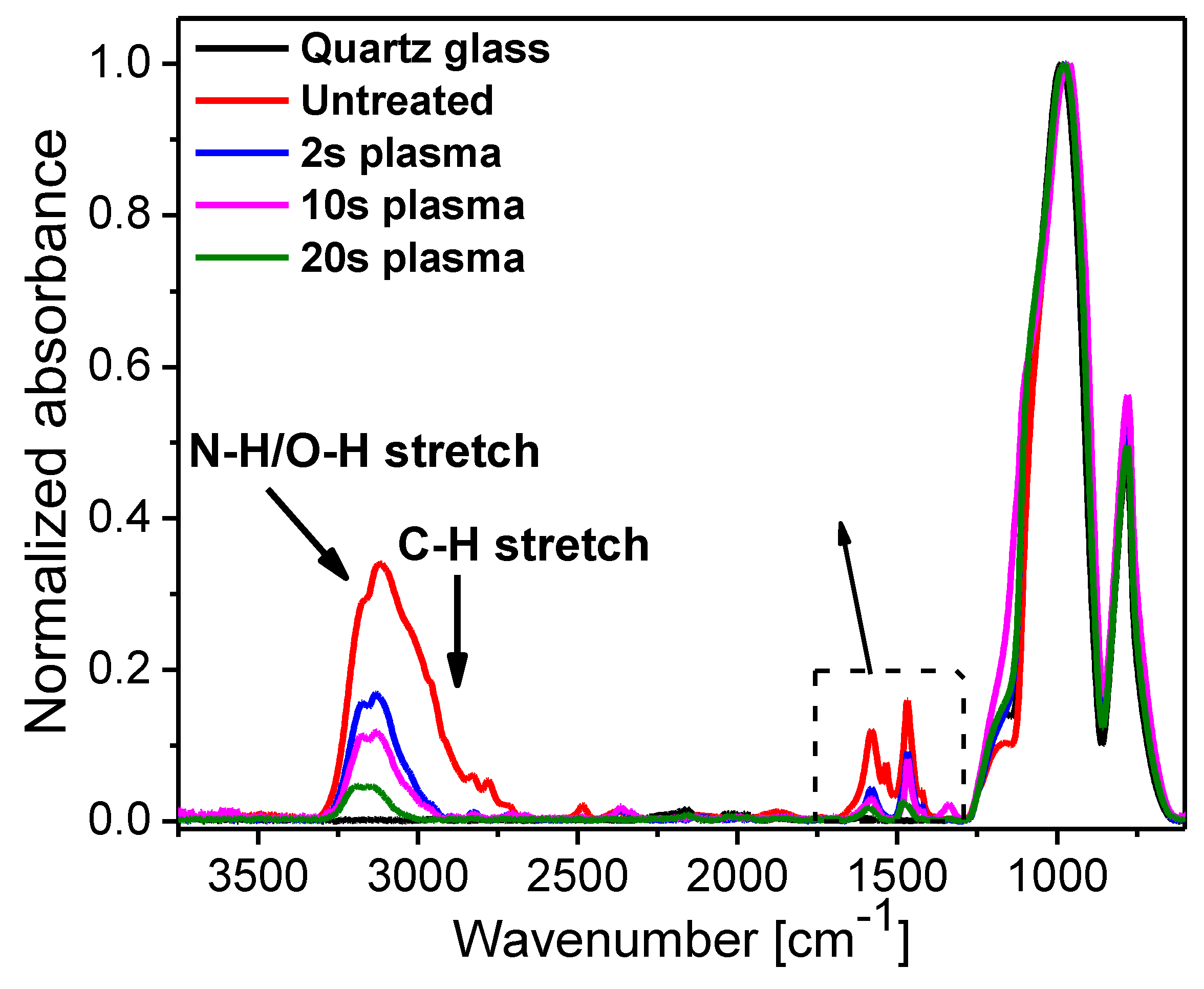
XPS revealed that ambient air plasma treatment partially removed carbon contamination, methylammonium cations, and halide anions from the surface of the mixed-halide perovskite films. ATR-FTIR measurement was employed further to investigate the effects of plasma treatment on the chemistry of mixed-halide perovskite; the ATR-FTIR patterns of the perovskite films appear in Figure 5. The peaks located at 1200–1700 cm−1 are related to C–N and C=O stretch, and the intensity of these peaks decreased dramatically after plasma treatment. In addition, the peak located at 2700–3000 cm−1 corresponded to C–H stretching, and its intensity fell to around zero after plasma treatment for 1 s. The treatment also reduced the intensity of the peak located at 3000–3300 cm−1, corresponding to N–H/O–H stretching. These results correlated well with the atomic concentrations obtained by XPS, showing that plasma treatment led to effective removal of the organic part of the mixed-halide perovskite films. Chemical analysis of the perovskite films indicated that ambient-air plasma treatment cleans surfaces and forms lead-rich perovskite films.
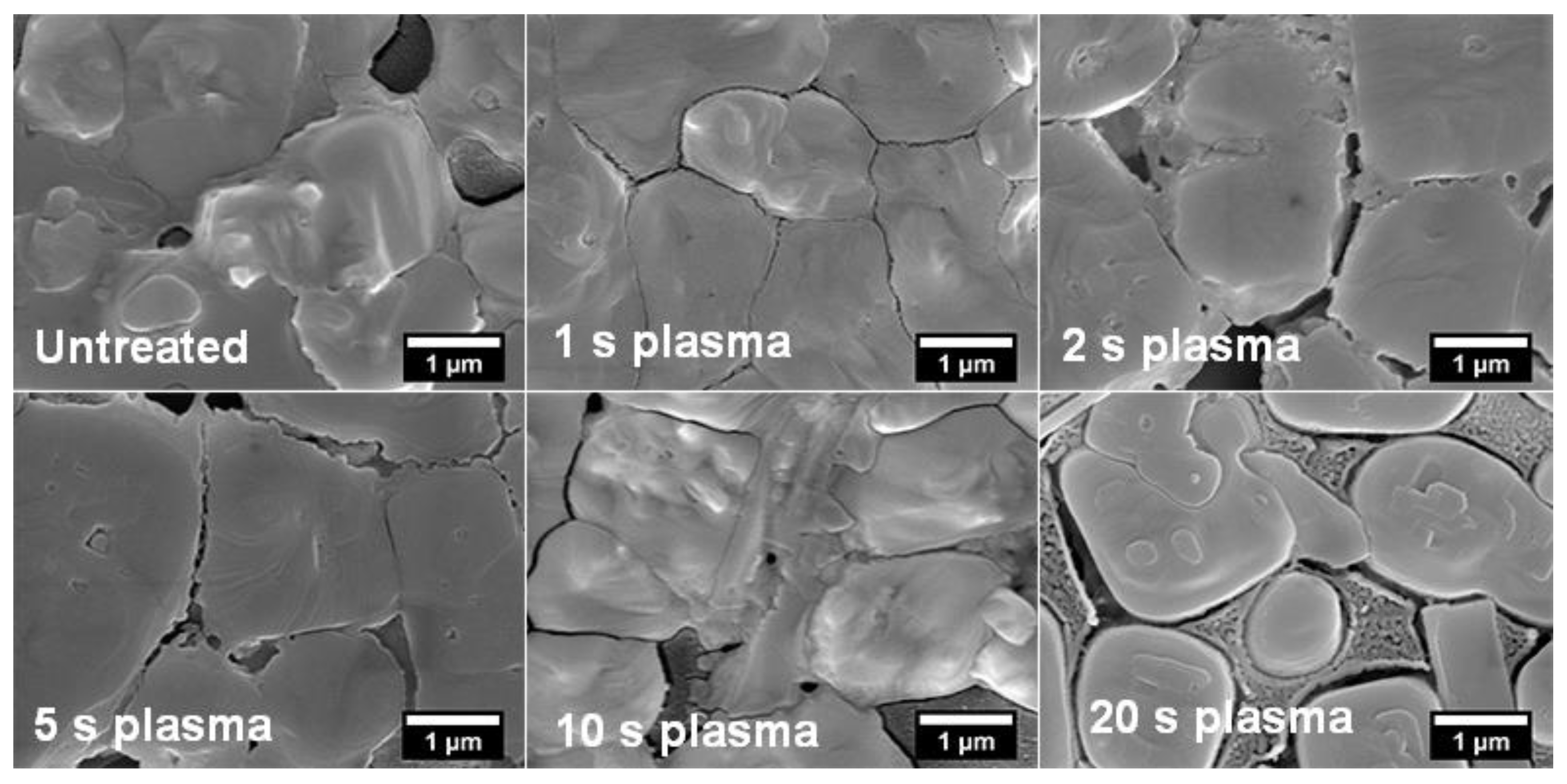
Scanning electron microscopy (SEM) was employed to evaluate the effect of plasma treatment on the surface morphology of the perovskite films (Figure 6). The surface of the “untreated” mixed-halide perovskite film shows the inhomogeneity and compactness of the grains. The non-homogeneous “untreated” surface may be explained by evaporation of the solvent of the perovskite precursor from the substrate. The perovskite precursor ink was a mixture of methylammonium iodide and lead chloride dissolved in dimethyl formamide. Once the perovskite had been spin-coated onto the substrate, the solvent evaporated very rapidly and generated non-uniform perovskite crystals [38]. Short plasma treatment (1 s) led to higher homogeneity of the surface as grain boundaries appeared. However, the sample treated for 1 s exhibited a number of shrunken grain boundaries. The same phenomena were reported by Cao et al. [19], who noted that defects in the grain boundaries of perovskite films appeared after microwave irradiation treatment, related to the decomposition of the perovskite film. These results accord with the XRD analysis, which revealed partial decomposition of the mixed-halide perovskite film after short plasma treatment of 1 s. The cracks became less after plasma treatment for 2 s and 5 s. Prolonging plasma treatment time after 5 s led to pin-holing and separation of the grains at the surface. The calculated average grain size from the SEM results are summarized in Table 1. It appears that short plasma treatment (≤5 s) led to extended grain sizes of the mixed-halide perovskite; the average grain size corresponding to the “untreated” film is ~0.92 and increased to 1.93 nm after 5 s plasma treatment. However, longer plasma treatments of 10 s and 20 s decreased the average grain size to ~0.78 nm and 0.54 nm, respectively, which can be related to the etching of the surface after longer plasma treatment. The thickness of the of mixed-halide perovskite films before and after plasma treatment was also investigated (Figure S4). The results demonstrated that, after 1 s and 2 s of exposure time, the thickness of the films decreased from approx. 229 nm to 225 nm and 218 nm. This may be related to the etching of organic contamination from the surface, and even of the organic component of the perovskite film itself. Longer plasma treatments (˃5 s) etched more of the surface and thickness decreased to approx. 200 nm after plasma treatment for 20 s, suggesting that the upper layer of the surface was removed.
4. Conclusions
Ambient air low-temperature plasma treatment was successfully applied to perovskite film for the first time. The effects of such plasma treatment on the opto-electronic properties, crystallization, and morphology of the perovskite film were investigated. Ambient-air plasma led to remarkable changes in the energy bands of the mixed-halide perovskite in a manner dependent on treatment time, i.e., short plasma treatment (≤5 s) led to widening the band gap and longer plasma treatment (˃5 s) led to narrowing the band gap. Plasma treatment can control the morphology of the perovskite film by changing grain boundaries and crystalline structure, leading to a uniform surface after short plasma treatment. However, prolonging plasma treatment leads to the separation of the grains and the film becomes non-homogeneous. The differences between the results of short and long plasma treatment were related to the etching of the perovskite film. Short plasma treatment had a minor etching effect on the surface, in contrast to longer treatment that etched the surface and penetrated to the bulk of the perovskite film and consequently led to slight etching of the surface. This contribution demonstrates that plasma treatment using DCSBD is a promising post-treatment technique for control of the surface properties of mixed-halide perovskite films. In addition, using ambient air as an operational gas, together with short treatment times, render plasma treatment by DCSBD a low-cost and rapid means of processing perovskite films.
Supplementary Materials
The following are available online at https://www.mdpi.com/2075-4701/9/9/991/s1, Figure S1: Photo of plasma treated perovskite films with different distances, Figure S2: Crystallite size of PbI2 at plate of (100) before and after plasma treatment, Figure S3: Variation of valance bands of mixed-halide perovskite film during plasma treatment, Figure S4: Variation the thickness of mixed-halide perovskite during plasma treatment time.
Author Contributions
Experiments and data analysis and draft preparation, M.S.; Data analysis and writing-editing, M.S. and T.H.; SEM measurements and morphology analysis, J.J., M.S.
Funding
This research was supported by project LO1411 (NPU I) funded by Ministry of Education Youth and Sports of Czech Republic. Part of the work was carried out at CEITEC Nano Research Infrastructure (MEYS CR, 2016–2019). The authors would like to thank the Grant Agency of Masaryk University. The work of Masoud Shekargoftar was also supported by Brno Ph.D. Talent Scholarship, funded by the City of Brno.
Acknowledgments
The authors would like to thank David Pavliňák, Monika Stupavská, Pavel Franta and Ondrej Caha for the acquired ATR-FTIR, XPS and UV-Vis data and XRD data. Tony Long (Svinošice) helped work up the English.
Conflicts of Interest
The authors declare no conflict of interest.
References
- Ava, T.T.; Al Mamun, A.; Marsillac, S.; Namkoong, G. A Review: Thermal Stability of Methylammonium Lead Halide Based Perovskite Solar Cells. Appl. Sci. 2019, 9, 188. [Google Scholar] [CrossRef]
- Li, H.; Zhu, K.; Zhang, K.; Huang, P.; Li, D.; Yuan, L.; Cao, T.; Sun, Z.; Li, Z.; Chen, Q.; et al. 3,4-Dihydroxybenzhydrazide as an additive to improve the morphology of perovskite films for efficient and stable perovskite solar cells. Org. Electron. 2019, 66, 47–52. [Google Scholar] [CrossRef]
- Wang, R.; Mujahid, M.; Duan, Y.; Wang, Z.-K.; Xue, J.; Yang, Y. A Review of Perovskites Solar Cell Stability. Adv. Funct. Mater. 2019, 1808843, 1–25. [Google Scholar] [CrossRef]
- Singh, R.; Singh, P.K.; Bhattacharya, B.; Rhee, H.-W. Review of current progress in inorganic hole-transport materials for perovskite solar cells. Appl. Mater. Today 2019, 14, 175–200. [Google Scholar] [CrossRef]
- Huang, F.; Li, M.; Siffalovic, P. Environmental Science From scalable solution fabrication of perovskite films towards commercialization of solar cells. Energy Environ. Sci. 2019, 12, 518–549. [Google Scholar] [CrossRef]
- Adjokatse, S.; Kardula, J.; Fang, H.-H.; Shao, S.; Brink, G.H.T.; Loi, M.A. Effect of the Device Architecture on the Performance of FA0.85MA0.15PbBr0.45I2.55 Planar Perovskite Solar Cells. Adv. Mater. Interfaces 2019, 6, 1801667. [Google Scholar] [CrossRef]
- Correa-Baena, J.-P.; Saliba, M.; Buonassisi, T.; Grätzel, M.; Abate, A.; Tress, W.; Hagfeldt, A. Promises and challenges of perovskite solar cells. Science 2017, 358, 739–744. [Google Scholar] [CrossRef] [Green Version]
- Zhou, Y.; Yang, M.; Game, O.S.; Wu, W.; Kwun, J.; Strauss, M.A.; Yan, Y.; Huang, J.; Zhu, K.; Padture, N.P. Manipulating Crystallization of Organolead Mixed-Halide Thin Films in Antisolvent Baths for Wide-Bandgap Perovskite Solar Cells. ACS Appl. Mater. Interfaces 2016, 8, 2232–2237. [Google Scholar] [CrossRef]
- Uribe, J.I.; Ciro, J.; Montoya, J.F.; Osorio, J.; Jaramillo, F. Enhancement of Morphological and Optoelectronic Properties of Perovskite Films by CH3NH3Cl Treatment for Efficient Solar Minimodules. ACS Appl. Energy Mater. 2018, 1, 1047–1052. [Google Scholar] [CrossRef]
- Chu, Z.; Yang, M.; Schulz, P.; Wu, D.; Ma, X.; Seifert, E.; Sun, L.; Li, X.; Zhu, K.; Lai, K. Impact of grain boundaries on efficiency and stability of organic-inorganic trihalide perovskites. Nat. Commun. 2017, 8, 2230. [Google Scholar] [CrossRef]
- Yu, Y.; Yang, S.; Lei, L.; Cao, Q.; Shao, J.; Zhang, S.; Liu, Y. Ultrasmooth Perovskite Film via Mixed Anti-Solvent Strategy with Improved Efficiency. ACS Appl. Mater. Interfaces 2017, 9, 3667–3676. [Google Scholar] [CrossRef] [PubMed]
- Huang, L.-B.; Su, P.-Y.; Liu, J.-M.; Huang, J.-F.; Chen, Y.-F.; Qin, S.; Guo, J.; Xu, Y.-W.; Su, C.-Y. Interface engineering of perovskite solar cells with multifunctional polymer interlayer toward improved performance and stability. J. Power Sources 2018, 378, 483–490. [Google Scholar] [CrossRef]
- Eperon, G.E.; Burlakov, V.M.; Docampo, P.; Goriely, A.; Snaith, H.J. Morphological control for high performance, solution-processed planar heterojunction perovskite solar cells. Adv. Funct. Mater. 2014, 24, 151–157. [Google Scholar] [CrossRef]
- Shi, D.; Adinolfi, V.; Comin, R.; Yuan, M.; Alarousu, E.; Buin, A.; Chen, Y.; Hoogland, S.; Rothenberger, A.; Katsiev, K.; et al. Low trap-state density and long carrier diffusion in organolead trihalide perovskite single crystals. Science 2015, 347, 519–522. [Google Scholar] [CrossRef] [PubMed] [Green Version]
- Yoo, H.-S.; Park, N.-G. Post-treatment of perovskite film with phenylalkylammonium iodide for hysteresis-less perovskite solar cells. Sol. Energy Mater. Sol. Cells 2018, 179, 57–65. [Google Scholar] [CrossRef]
- Dong, G.; Xia, D.; Yang, Y.; Sheng, L.; Su, T.; Fan, R.; Shi, Y.; Wang, J. Inverted thermal annealing of perovskite films: A method for enhancing photovoltaic device efficiency. RSC Adv. 2016, 6, 44034–44040. [Google Scholar] [CrossRef]
- Masood, M.T.; Weinberger, C.; Sarfraz, J.; Rosqvist, E.; Sandén, S.; Sandberg, O.J.; Vivo, P.; Hashmi, G.; Lund, P.D.; Österbacka, R.; et al. Impact of Film Thickness of Ultrathin Dip-Coated Compact TiO2 Layers on the Performance of Mesoscopic Perovskite Solar Cells. ACS Appl. Mater. Interfaces 2017, 9, 17906–17913. [Google Scholar] [CrossRef] [PubMed]
- Zhang, R.; Ling, H.; Lu, X.; Xia, J. The facile modification of PEDOT: PSS buffer layer by polyethyleneglycol and their effects on inverted perovskite solar cell. Sol. Energy 2019, 186, 398–403. [Google Scholar] [CrossRef]
- Cao, Q.; Yang, S.; Gao, Q.; Lei, L.; Yu, Y.; Shao, J.; Liu, Y. Fast and Controllable Crystallization of Perovskite Films by Microwave Irradiation Process. ACS Appl. Mater. Interfaces 2016, 8, 7854–7861. [Google Scholar] [CrossRef]
- Ren, Z.; Ng, A.; Shen, Q.; Gokkaya, H.C.; Wang, J.; Yang, L.; Yiu, W.-K.; Bai, G.; Djurišić, A.B.; Leung, W.W.-F.; et al. Thermal Assisted Oxygen Annealing for High Efficiency Planar CH3NH3PbI3 Perovskite Solar Cells. Sci. Rep. 2014, 4, 6752. [Google Scholar] [CrossRef]
- Yang, Y.; Feng, S.; Li, M.; Xu, W.; Yin, G.; Wang, Z.; Sun, B.; Gao, X. Annealing Induced Re-crystallization in CH3NH3PbI3−xClx for High Performance Perovskite Solar Cells. Sci. Rep. 2017, 7, 46724. [Google Scholar] [CrossRef] [PubMed]
- Xiao, X.; Bao, C.; Fang, Y.; Dai, J.; Ecker, B.R.; Wang, C.; Lin, Y.; Tang, S.; Liu, Y.; Deng, Y.; et al. Argon Plasma Treatment to Tune Perovskite Surface Composition for High Efficiency Solar Cells and Fast Photodetectors. Adv. Mater. 2018, 30, 1705176. [Google Scholar] [CrossRef] [PubMed]
- Zheng, W.; Lin, Y.; Zhang, Y.; Yang, J.; Peng, Z.; Liu, A.; Zhang, F.; Hou, L. Dual Function of UV/Ozone Plasma-Treated Polymer in Polymer/Metal Hybrid Electrodes and Semitransparent Polymer Solar Cells. ACS Appl. Mater. Interfaces 2017, 9, 44656–44666. [Google Scholar] [CrossRef] [PubMed] [Green Version]
- Wang, K.; Zhao, W.; Liu, J.; Niu, J.; Liu, Y.; Ren, X.; Feng, J.; Liu, Z.; Sun, J.; Wang, D.; et al. CO2 Plasma-Treated TiO2 Film as an Effective Electron Transport Layer for High-Performance Planar Perovskite Solar Cells. ACS Appl. Mater. Interfaces 2017, 9, 33989–33996. [Google Scholar] [CrossRef] [PubMed]
- Masood, M.T.; Weinberger, C.; Qudsia, S.; Rosqvist, E.; Sandberg, O.J.; Nyman, M.; Sandén, S.; Vivo, P.; Aitola, K.; Lund, P.D.; et al. Influence of titanium dioxide surface activation on the performance of mesoscopic perovskite solar cells. Thin Solid Films 2019, 686, 137418. [Google Scholar] [CrossRef]
- Černák, M.; Kováčik, D.; Ráhel’, J.; St’ahel, P.; Zahoranová, A.; Kubincová, J.; Tóth, A.; Černáková, L. Generation of a high-density highly non-equilibrium air plasma for high-speed large-area flat surface processing. Plasma Phys. Control. Fusion 2011, 53, 124031. [Google Scholar] [CrossRef]
- Medvecká, V.; Kováčik, D.; Zahoranová, A.; Černák, M. Atmospheric pressure plasma assisted calcination by the preparation of TiO2 fibers in submicron scale. Appl. Surf. Sci. 2018, 428, 609–615. [Google Scholar] [CrossRef]
- Mudra, E.; Streckova, M.; Pavlinak, D.; Medvecka, V.; Kovacik, D.; Kovalcikova, A.; Zubko, P.; Girman, V.; Dankova, Z.; Koval, V.; et al. Development of Al2O3 electrospun fibers prepared by conventional sintering method or plasma assisted surface calcination. Appl. Surf. Sci. 2017, 415, 90–98. [Google Scholar] [CrossRef]
- Kováčik, D.; Medvecká, V.; Tucekova, Z.; Zahoranova, A.; Cernak, M. Atmospheric pressure plasma assisted calcination of composite submicron fibers. Eur. Phys. J. Appl. Phys. 2016, 75, 24715. [Google Scholar]
- Medvecká, V.; Kováčik, D.; Zahoranová, A.; Stupavská, M.; Černák, M. Atmospheric pressure plasma assisted calcination of organometallic fibers. Mater. Lett. 2016, 162, 79–82. [Google Scholar] [CrossRef]
- Shekargoftar, M.; Dzik, P.; Stupavska, M.; Pavlinak, D.; Homola, T. Mineralization of flexible mesoporous TiO2 photoanodes using two low-temperature DBDs in ambient air. Contrib. Plasma Phys. 2018, 59, 102–110. [Google Scholar] [CrossRef]
- Homola, T.; Shekargoftar, M.; Dzik, P.; Krumpolec, R.; Ďurašová, Z.; Veselý, M.; Černák, M. Low-temperature (70 °C) ambient air plasma-fabrication of inkjet-printed mesoporous TiO2 flexible photoanodes. Flex. Print. Electron. 2017, 2, 35010. [Google Scholar] [CrossRef]
- Homola, T.; Pospišil, J.; Krumpolec, R.; Souček, P.; Dzik, P.; Weiter, M.; Černák, M. Atmospheric Dry Hydrogen Plasma Reduction of Inkjet-Printed Flexible Graphene Oxide Electrodes. ChemSusChem 2018, 11, 941–947. [Google Scholar] [CrossRef] [PubMed]
- Zhou, L.; Chang, J.; Liu, Z.; Sun, X.; Lin, Z.; Chen, D.; Zhang, C.; Zhang, J.; Hao, Y. Enhanced planar perovskite solar cell efficiency and stability using a perovskite/PCBM heterojunction formed in one step. Nanoscale 2018, 10, 3053–3059. [Google Scholar] [CrossRef] [PubMed]
- Dubey, A.; Adhikari, N.; Mabrouk, S.; Wu, F.; Chen, K.; Yang, S.; Qiao, Q. A strategic review on processing routes towards highly efficient perovskite solar cells. J. Mater. Chem. A 2018, 6, 2406–2431. [Google Scholar] [CrossRef]
- Lu, J.G.; Fujita, S.; Kawaharamura, T.; Nishinaka, H.; Kamada, Y.; Ohshima, T.; Ye, Z.Z.; Zeng, Y.J.; Zhang, Y.Z.; Zhu, L.P.; et al. Carrier concentration dependence of band gap shift in n-type ZnO:Al films. J. Appl. Phys. 2007, 101, 083705. [Google Scholar] [CrossRef]
- Shekargoftar, M.; Krumpolec, R.; Homola, T. Enhancement of electrical properties of flexible ITO/PET by atmospheric pressure roll-to-roll plasma. Mater. Sci. Semicond. Process. 2018, 75, 95–102. [Google Scholar] [CrossRef]
- Li, X.; Li, L.; Ma, Z.; Huang, J.; Ren, F. Low-cost synthesis, fluorescent properties, growth mechanism and structure of CH3NH3PbI3 with millimeter grains. Optik 2017, 142, 293–300. [Google Scholar] [CrossRef]
Figure 1.
(a) XRD pattern of perovskite film before and after plasma treatment. Denoted peaks with * correspond to the intermediate phase. (b) The location of some perovskite planes in the unit cell.
Figure 1.
(a) XRD pattern of perovskite film before and after plasma treatment. Denoted peaks with * correspond to the intermediate phase. (b) The location of some perovskite planes in the unit cell.
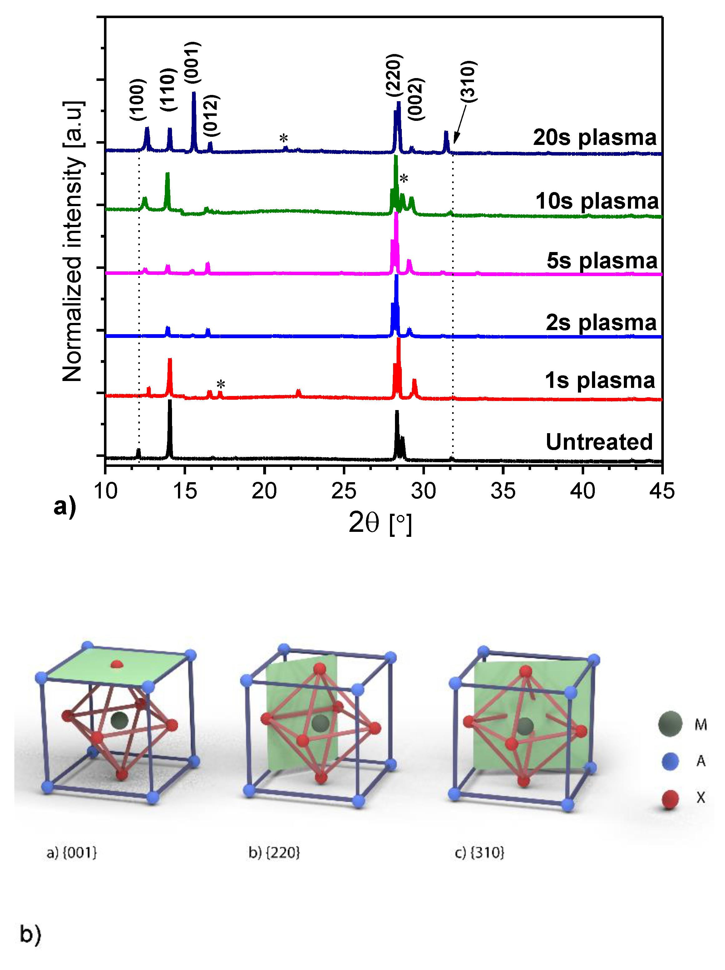
Figure 2.
UV–VIS absorbance spectra of the mixed-halide perovskite film before and after plasma treatment.
Figure 2.
UV–VIS absorbance spectra of the mixed-halide perovskite film before and after plasma treatment.
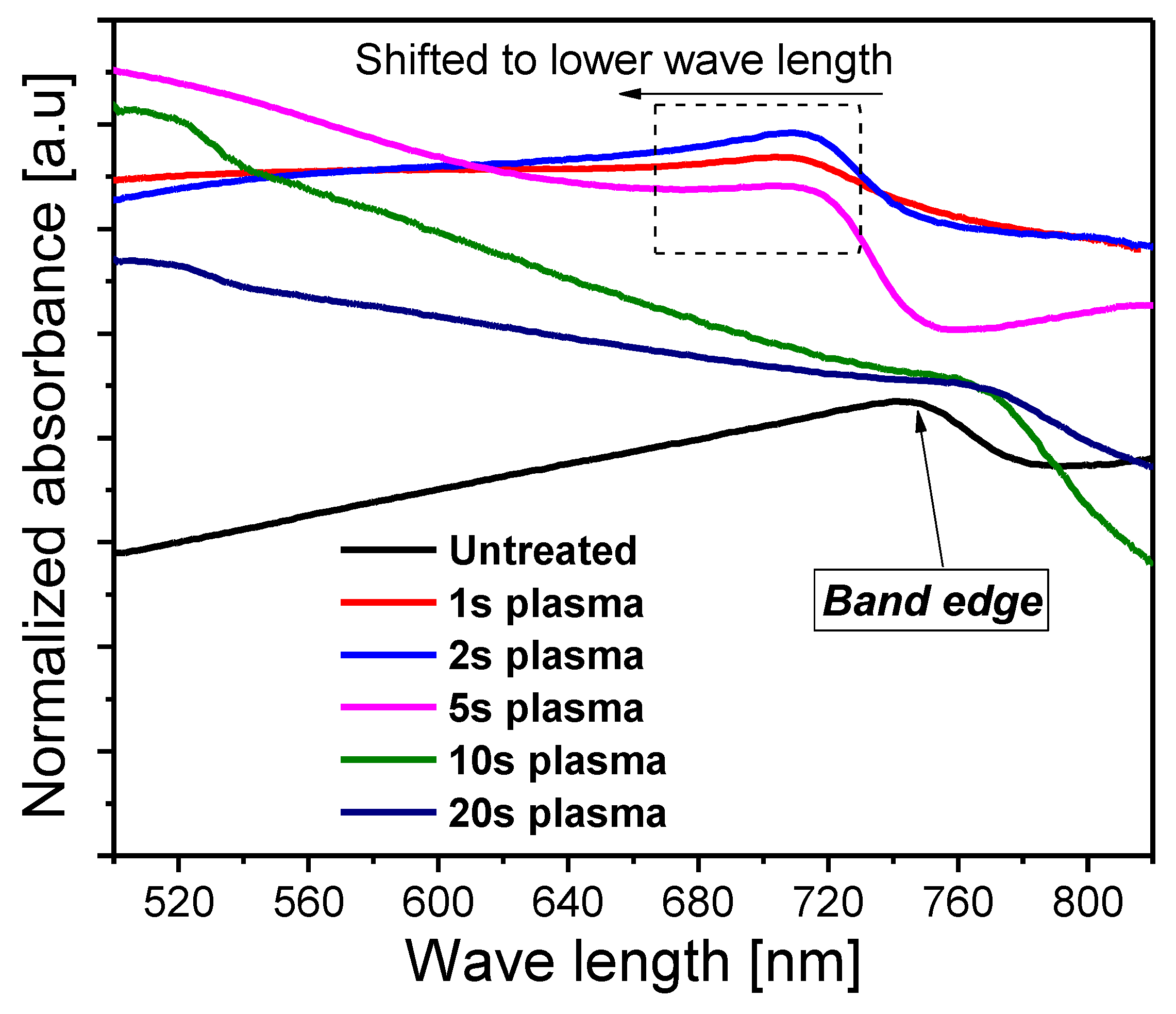
Figure 3.
Secondary electron (SE) onset of the mixed-halide perovskite film obtained by UPS before and after plasma treatment.
Figure 3.
Secondary electron (SE) onset of the mixed-halide perovskite film obtained by UPS before and after plasma treatment.

Figure 4.
(a) Band energy diagram, with corresponding views from above of the mixed-halide perovskite film before and after plasma treatment. (b) Atomic concentration of elements in perovskite films calculated from XPS survey spectra.
Figure 4.
(a) Band energy diagram, with corresponding views from above of the mixed-halide perovskite film before and after plasma treatment. (b) Atomic concentration of elements in perovskite films calculated from XPS survey spectra.

Figure 5.
ATR-FTIR pattern of mixed-halide perovskite film before and after plasma treatment.

Figure 6.
SEM images of mixed-halide perovskite films before and after plasma treatment.


Table 1.
Average grain size of the mixed-halide perovskite films before and after plasma treatment.
| Sample | Grain Size (µm) |
|---|---|
| Untreated | 0.92 |
| 1 s plasma | 1.36 |
| 2 s plasma | 1.81 |
| 5 s plasma | 1.93 |
| 10 s plasma | 0.78 |
| 20 s plasma | 0.54 |
© 2019 by the authors. Licensee MDPI, Basel, Switzerland. This article is an open access article distributed under the terms and conditions of the Creative Commons Attribution (CC BY) license (http://creativecommons.org/licenses/by/4.0/).
Share and Cite
MDPI and ACS Style
Shekargoftar, M.; Jurmanová, J.; Homola, T. A Study on the Effect of Ambient Air Plasma Treatment on the Properties of Methylammonium Lead Halide Perovskite Films. Metals 2019, 9, 991. https://doi.org/10.3390/met9090991
AMA Style
Shekargoftar M, Jurmanová J, Homola T. A Study on the Effect of Ambient Air Plasma Treatment on the Properties of Methylammonium Lead Halide Perovskite Films. Metals. 2019; 9(9):991. https://doi.org/10.3390/met9090991
Chicago/Turabian StyleShekargoftar, Masoud, Jana Jurmanová, and Tomáš Homola. 2019. "A Study on the Effect of Ambient Air Plasma Treatment on the Properties of Methylammonium Lead Halide Perovskite Films" Metals 9, no. 9: 991. https://doi.org/10.3390/met9090991
Note that from the first issue of 2016, this journal uses article numbers instead of page numbers. See further details here.