3. Results and Discussion
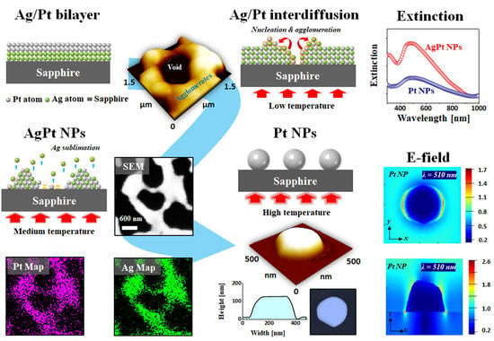
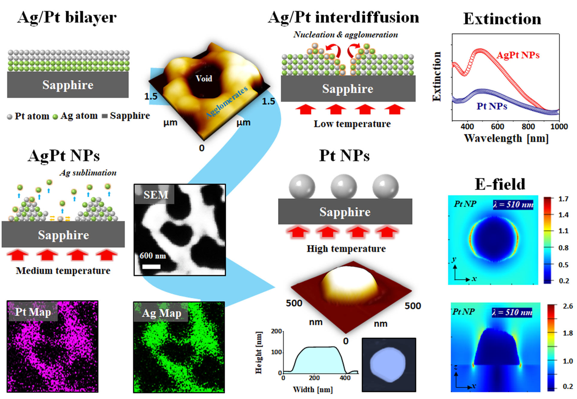
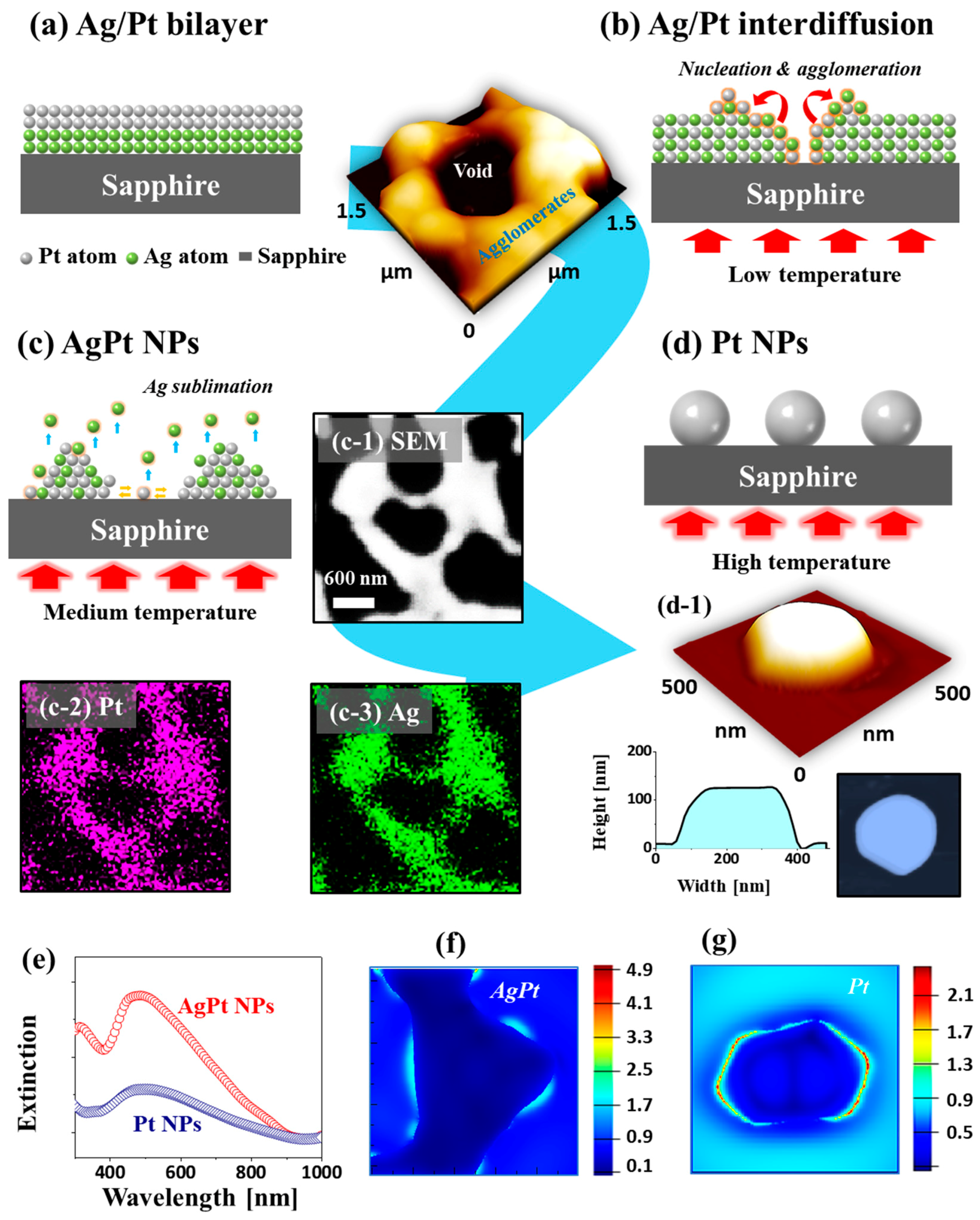
Figure 1 shows the fabrication steps of self-assembled Ag–Pt and Pt nanostructures on sapphire (0001) through the annealing of Ag–Pt bilayers. The formation of isolated NPs from the Ag–Pt bilayer films at successive annealings below the melting point of Ag and Pt can be discussed based on solid state dewetting (SSD), as described in
Figure 1a–d. In the case of the monometallic films, the dewetting process was mainly governed by the temperature-driven diffusion of atoms, i.e., the higher diffusivity yielded a higher dewetting rate and thus well-developed surface NPs. In previous studies, due to the low diffusivity of Pt atoms, interconnected and irregular Pt NPs were fabricated with pure Pt thin films on sapphire even at an annealing temperature (
Ta) above 800 °C [
23]. Meanwhile, well-developed and isolated Ag NPs were demonstrated under similar growth conditions with Ag films [
24]. The SSD of the bilayers involved additional mechanisms such as interdiffusion, alloying, and diffusion in the alloy phase, as shown in
Figure 1b,c, and thus the dewetting process and resulting nanostructures could be drastically different from the monometallic films [
25,
26]. In general, due to the broad miscibility gap between Ag and Pt and the large difference in the melting point of Ag (961.8 °C) and Pt (1768 °C), Ag–Pt alloy formation in the bulk phase is challenging [
26]. However, with nanoscale Ag–Pt bilayers, the intermixing of Ag and Pt atoms could sufficiently occur at
Ta, way below the melting point, due to the atomic interdiffusion at the Ag–Pt interface, as illustrated in
Figure 1b. This could lead to the alloying of Ag–Pt atoms, and thus the global diffusion of the atoms could be much increased. Eventually, the SSD could begin through the nucleation of voids and the accumulation of diffusing atoms, which resulted in the evolution of Ag–Pt alloy NPs at an intermediate
Ta, as shown in
Figure 1c. This process could be driven by the surface and interface energy minimization between film and substrate. Meanwhile, with further increased
Ta, the evolution of Ag–Pt alloy NPs could be attributed to the sublimation of Ag atoms because of the high vapor pressure of Ag at temperatures above 500 °C. This eventually could result in the formation of pure Pt NPs, as illustrated in
Figure 1d. These pure Pt NPs (obtained at a
Ta above 650 °C) could be expected to differ largely in terms of structure and LSPR response from pure Pt dewetting, as presented in the typical extinction spectra and local e-field of NPs in
Figure 1e–g.
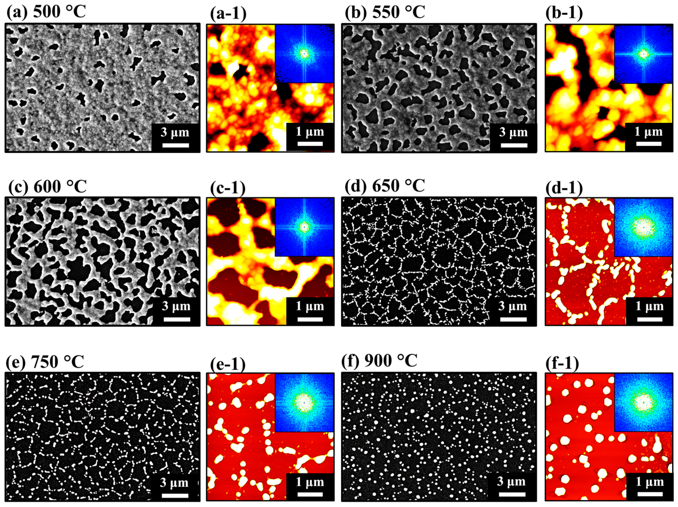
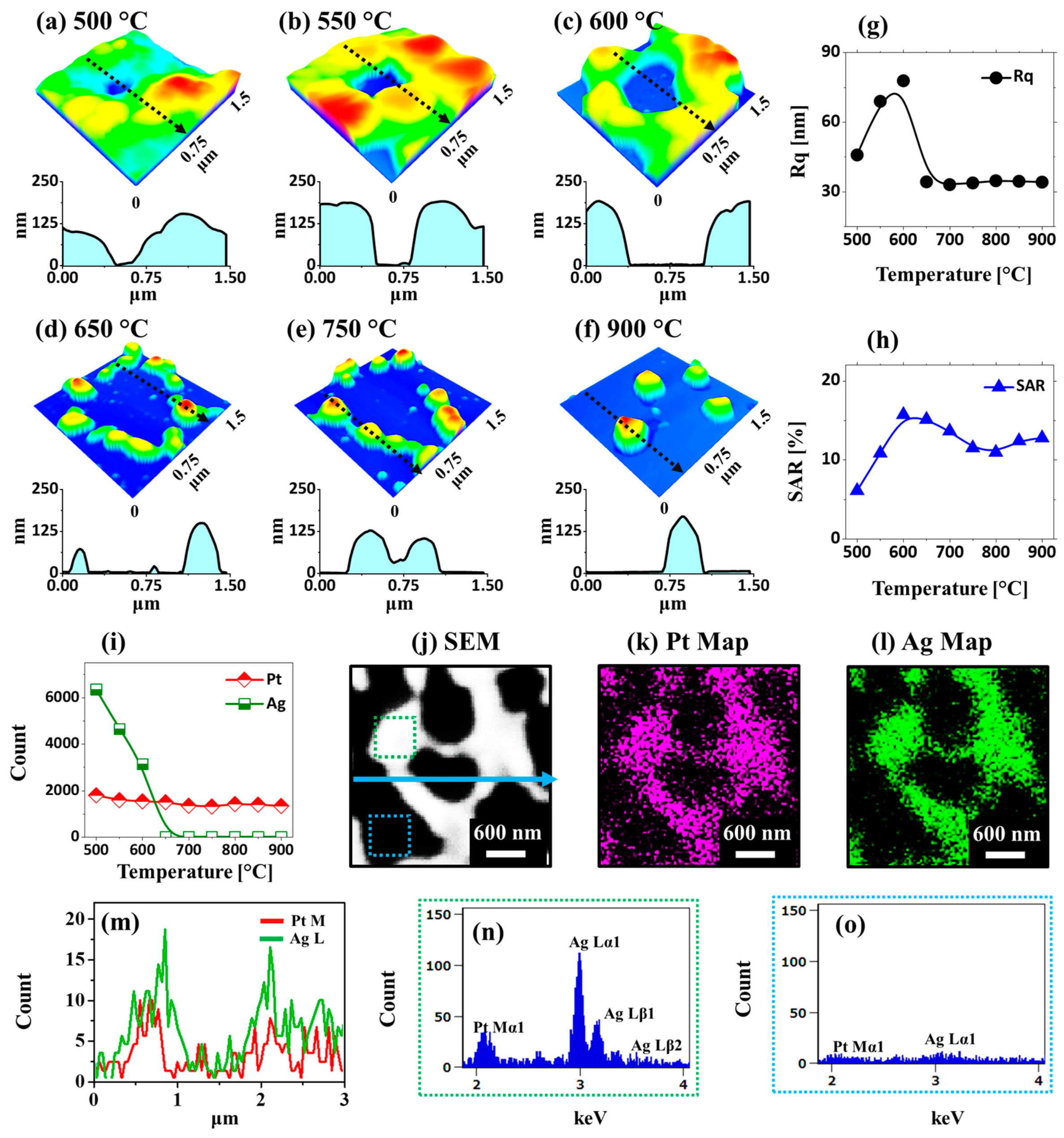
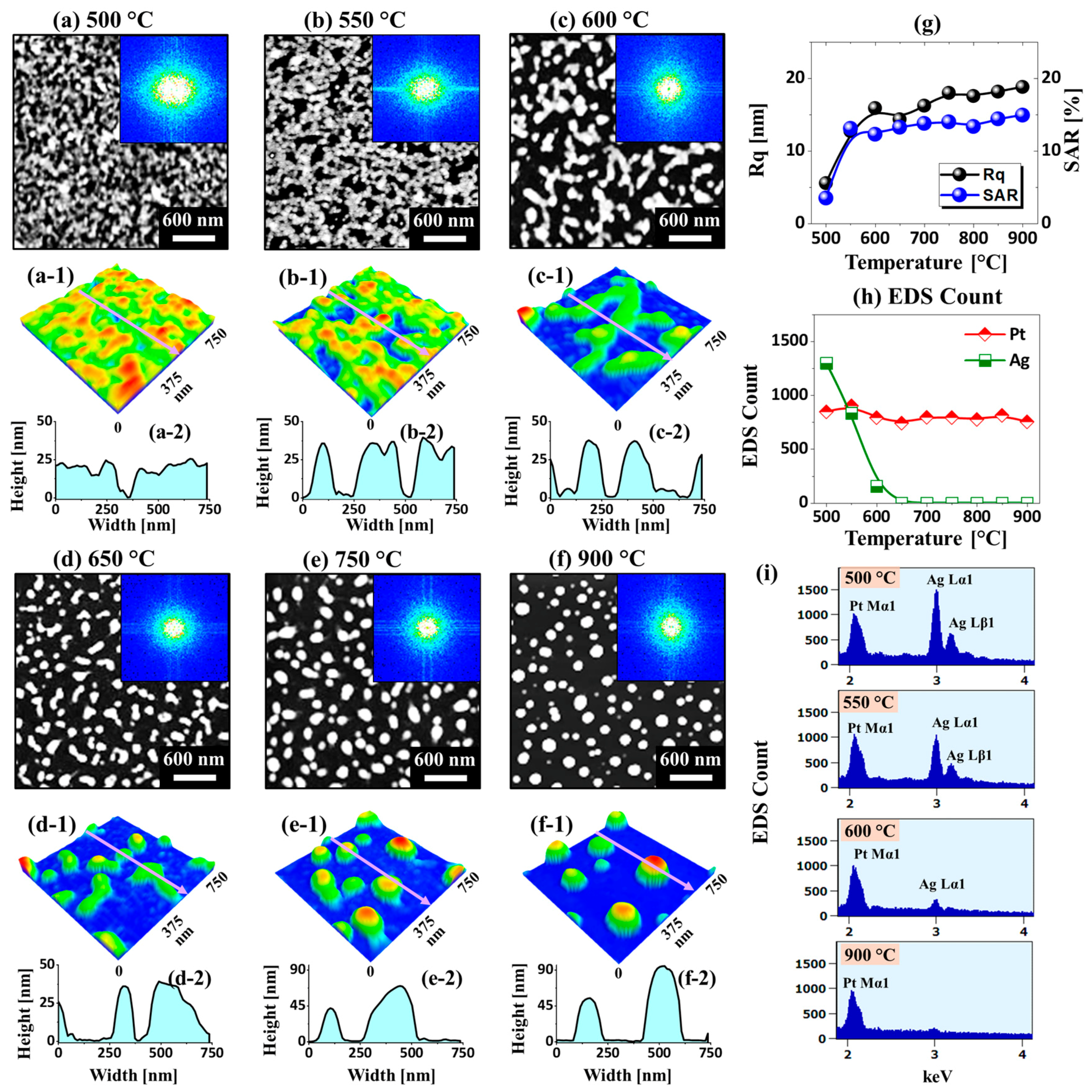
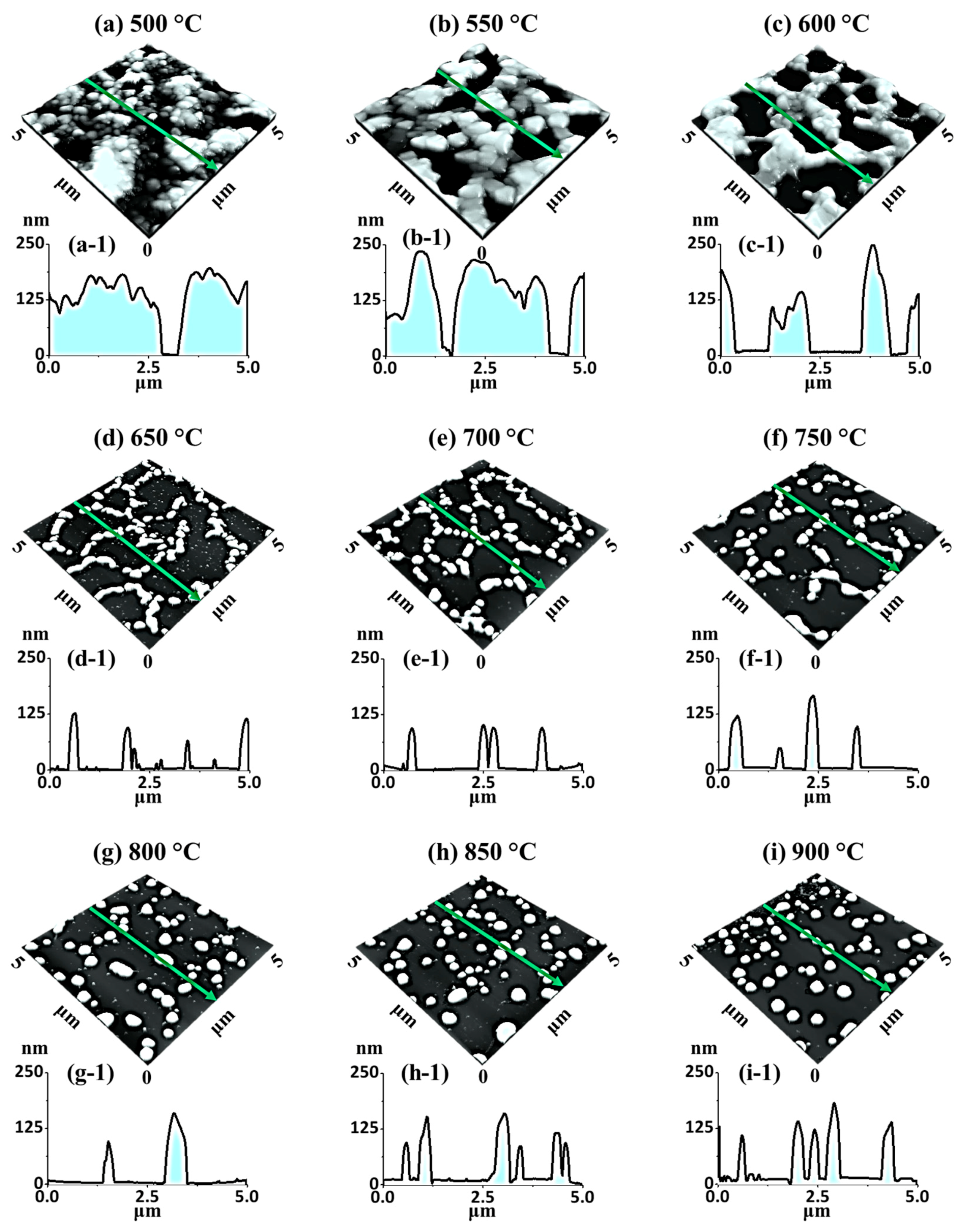
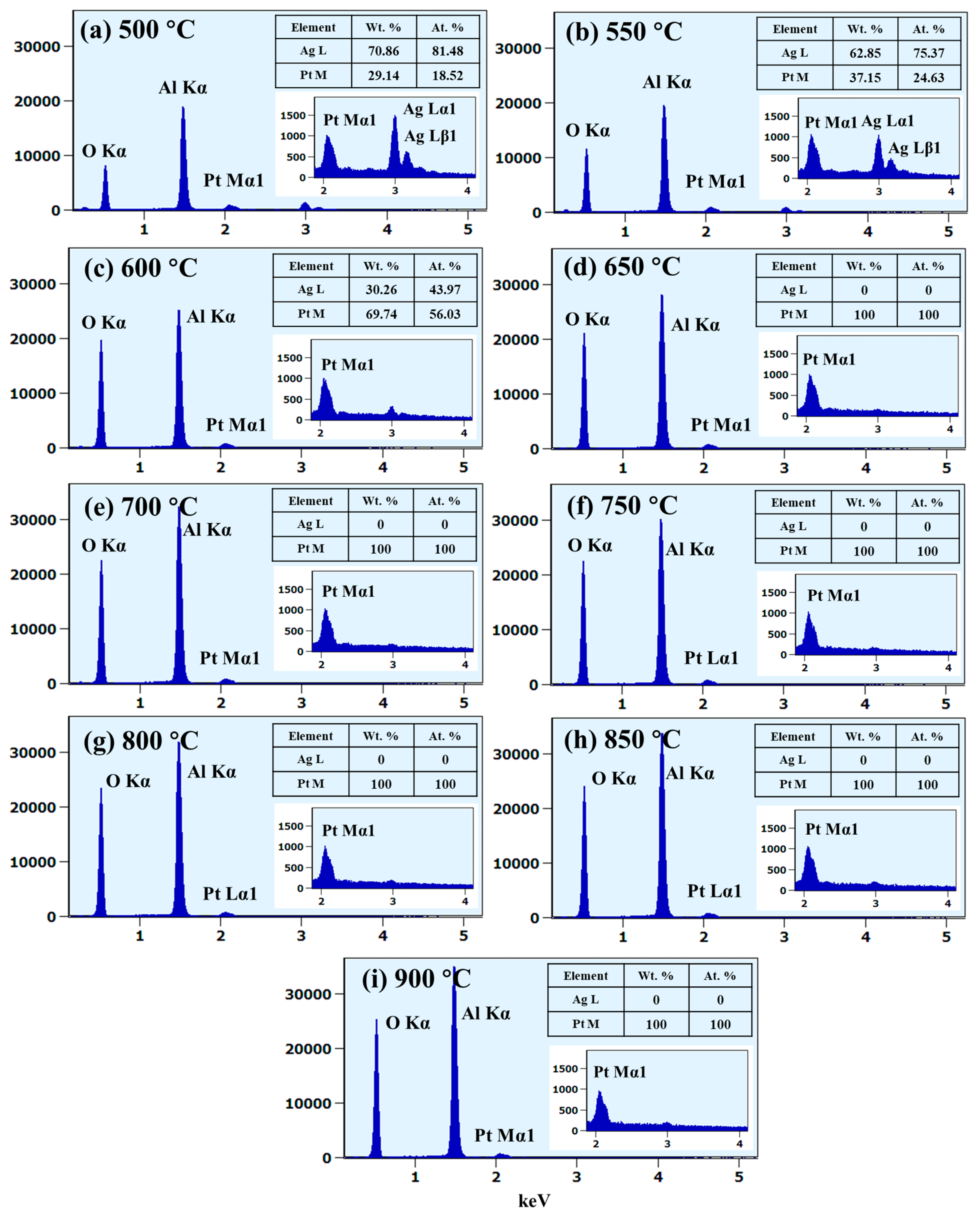
Figure 2 and
Figure 3 show the detailed morphological and elemental evolution of various Ag–Pt and Pt NPs in Ag
70 nm/Pt
15 nm bilayers with SEM, AFM, and EDS characterizations. The nanoscale voids and granular structures were formed as an initial stage of dewetting at 500 °C, as displayed in
Figure 2a and
Figure 3a. These pinholes and voids could preferentially form at the low-energy sites and grow larger due to adatom diffusion as well as the coalescence of atomic vacancies. The void growth rate (
depends upon the atomic diffusivity and thickness of the film according to the relation
, where
tDs,
vs,
Ω, γ, fv, and
h are diffusivity, the surface density of the atoms, atomic volume, surface energy, and film thickness, respectively [
27]. Thus, along with the increased
Ta between 550 and 600 °C at a constant film thickness, the
Ds increased correspondingly, causing vacancy coalescence. This resulted in the formation of larger voids more than 1 µm in width and network-like Ag–Pt nanostructures 200 nm in height, as displayed in
Figure 2b,c and
Figure 3b,c.
The surface evolution was also reflected in terms of a Fourier-filter transform (FFT) pattern, root mean squared (RMS) roughness (
Rq), and the surface area ratio (SAR) as a function of
Ta. The FFT patterns were gradually enlarged due to height fluctuation along with the evolution of voids. Similarly, increments of
Rq and SAR with temperature were observed, as shown in
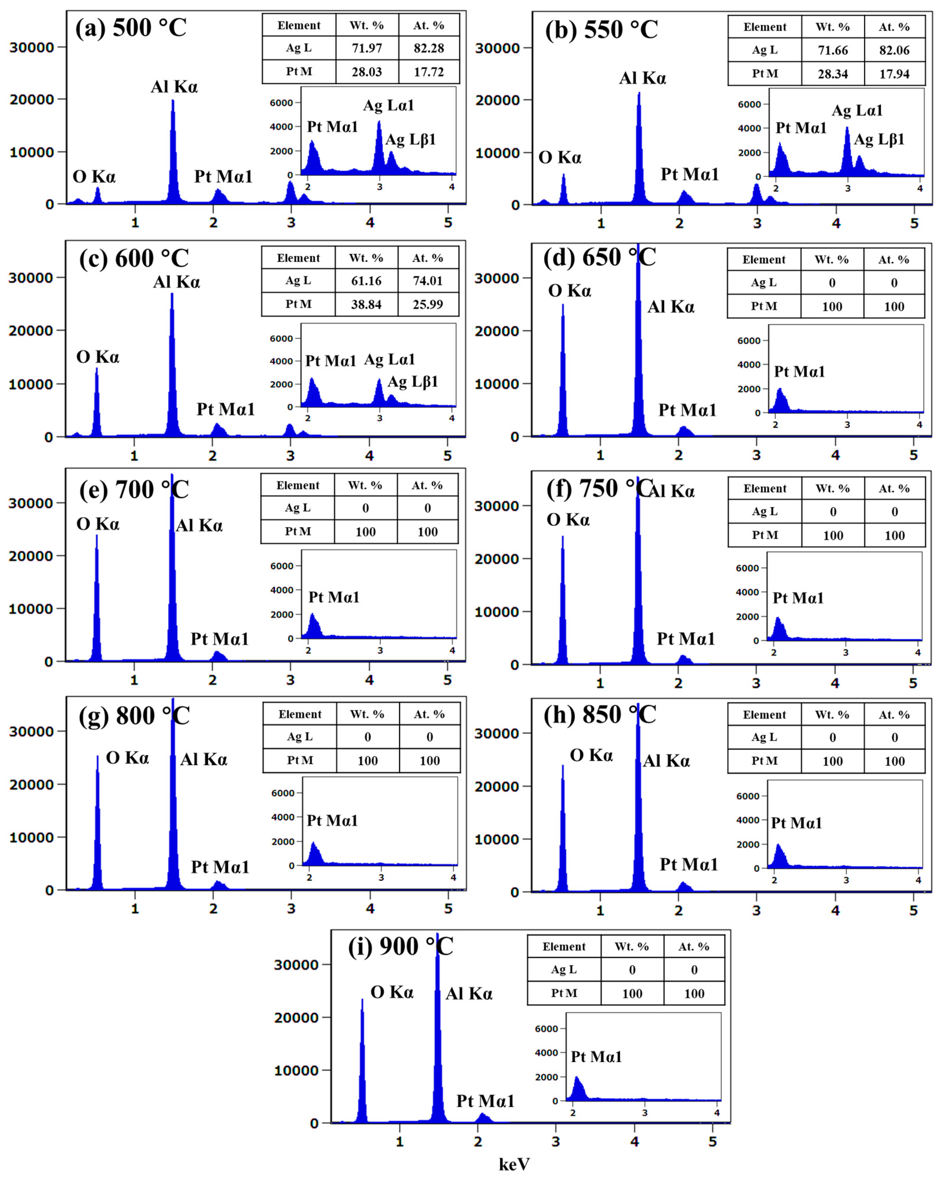
Figure 3g,h, which indicates an increase in the average surface height and area due to the formation of 3D Ag–Pt nanoclusters on the layered films. Meanwhile, along with the increased dewetting rate, the evolution of Ag–Pt nanoclusters could be affected by the sublimation of Ag atoms due to their high vapor pressure, as mentioned. To confirm the sublimation of Ag atoms in the alloy nanostructures, an elemental analysis on each sample was performed using an EDS measurement, as shown in
Figure 3i. The EDS counts of Pt Mα1 appeared to be similar, while the Ag Mα1 counts were sharply reduced between 500 and 600 °C, indicating the sublimation of Ag atoms. The sublimation rate of Ag also depended on the temperature and vapor pressure, as given by the relation
Rs = (3.513 × 10
22) (
T·
MAg)
−1/2 ×
Peq, where
Rs is the rate of sublimation,
T is temperature,
MAg is the molecular weight of silver, and
Peq is the equilibrium vapor pressure of Ag [
28,
29]. In the vapor pressure versus temperature curve,
Peq exponentially increased with temperature. Thus, the Ag atoms could abruptly sublimate with the increased
Ta, and pure Pt could be formed.
Furthermore, elemental distribution and alloy formation in the Ag–Pt nanoclusters were investigated in detail with the sample at 600 °C, as shown in
Figure 3j–o. The SEM image and Pt and Ag phase maps in
Figure 3j–l matched perfectly, indicating the homogeneous mixture of Ag and Pt in the nanostructures. This can also be seen in the EDS line profile extracted from an Ag–Pt nanocluster in
Figure 3m. In addition, the EDS spectra of the nanostructure region clearly show the Pt and Ag peaks, while the void region has no Ag and Pt peaks, as shown in
Figure 3n,o, respectively. As the Ag atoms were completely sublimated above 600 °C, the surface morphology was drastically transformed such that patterned and partially segmented Pt NPs were obtained at 650 °C, as shown in
Figure 2d and
Figure 3d. The fragmentation of isolated patterned Pt NPs from the connected nanocluster could have been due to Rayleigh-like instability [
27]. When
Ta was increased between 750 and 900 °C, the patterned Pt NPs were further isolated and became more uniform, as displayed in
Figure 2e,f, which demonstrated a unique morphological evolution compared to pure Pt dewetting [
23,
24]. This could have been correlated with the combinational effects of Ag–Pt alloying, the enhanced surface diffusion of atoms, the sublimation of Ag, and surface energy minimization [
30]. Since the average vertical size and surface area of Pt NPs were significantly decreased compared to the Ag–Pt nanoclusters,
Rq and the SAR were also sharply decreased. At the higher
Ta,
Rq and the SAR were found to be similar or slightly increased, likely due to the mild growth of Pt NPs.
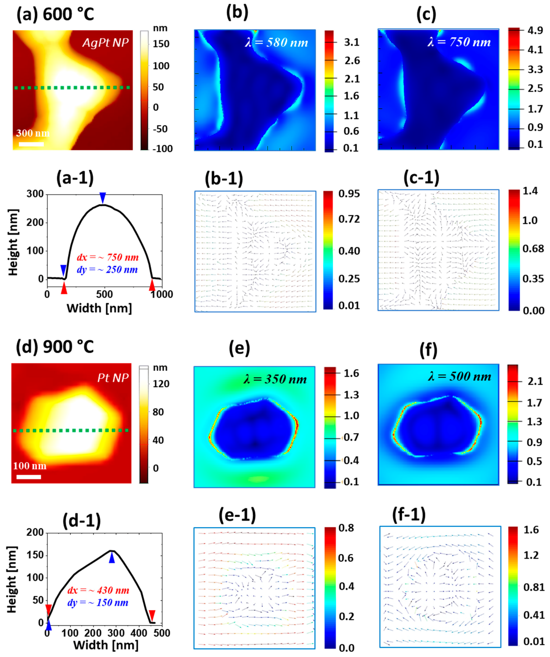
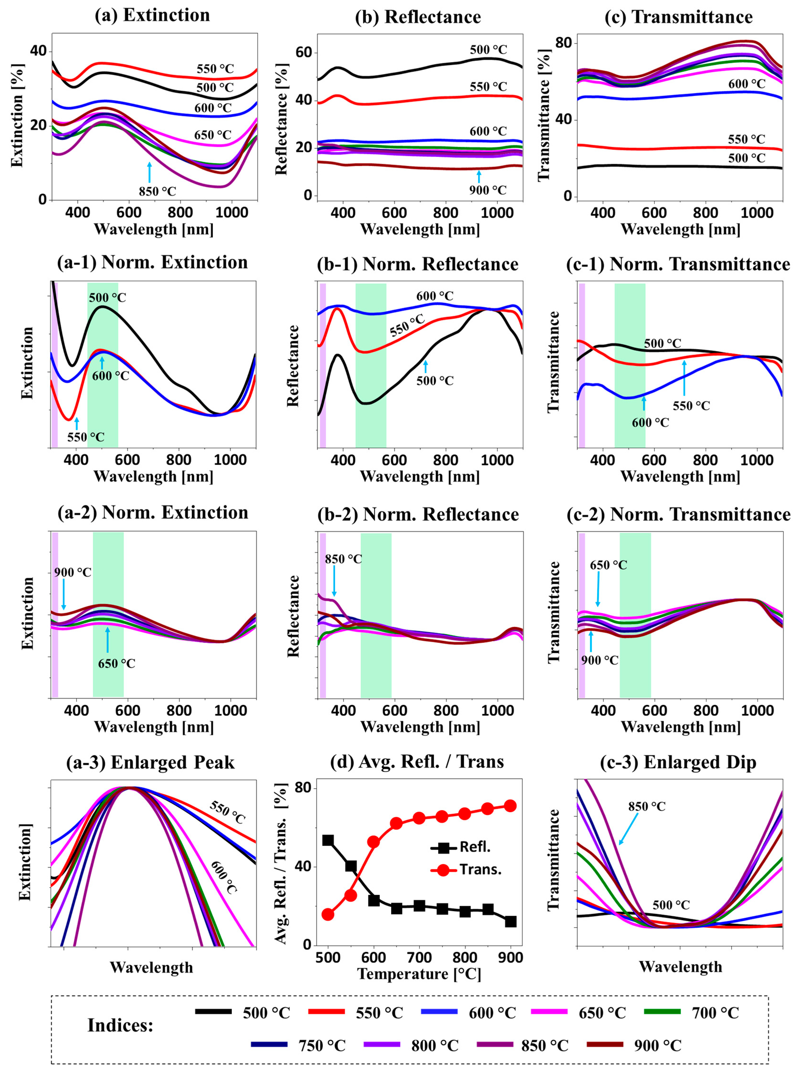
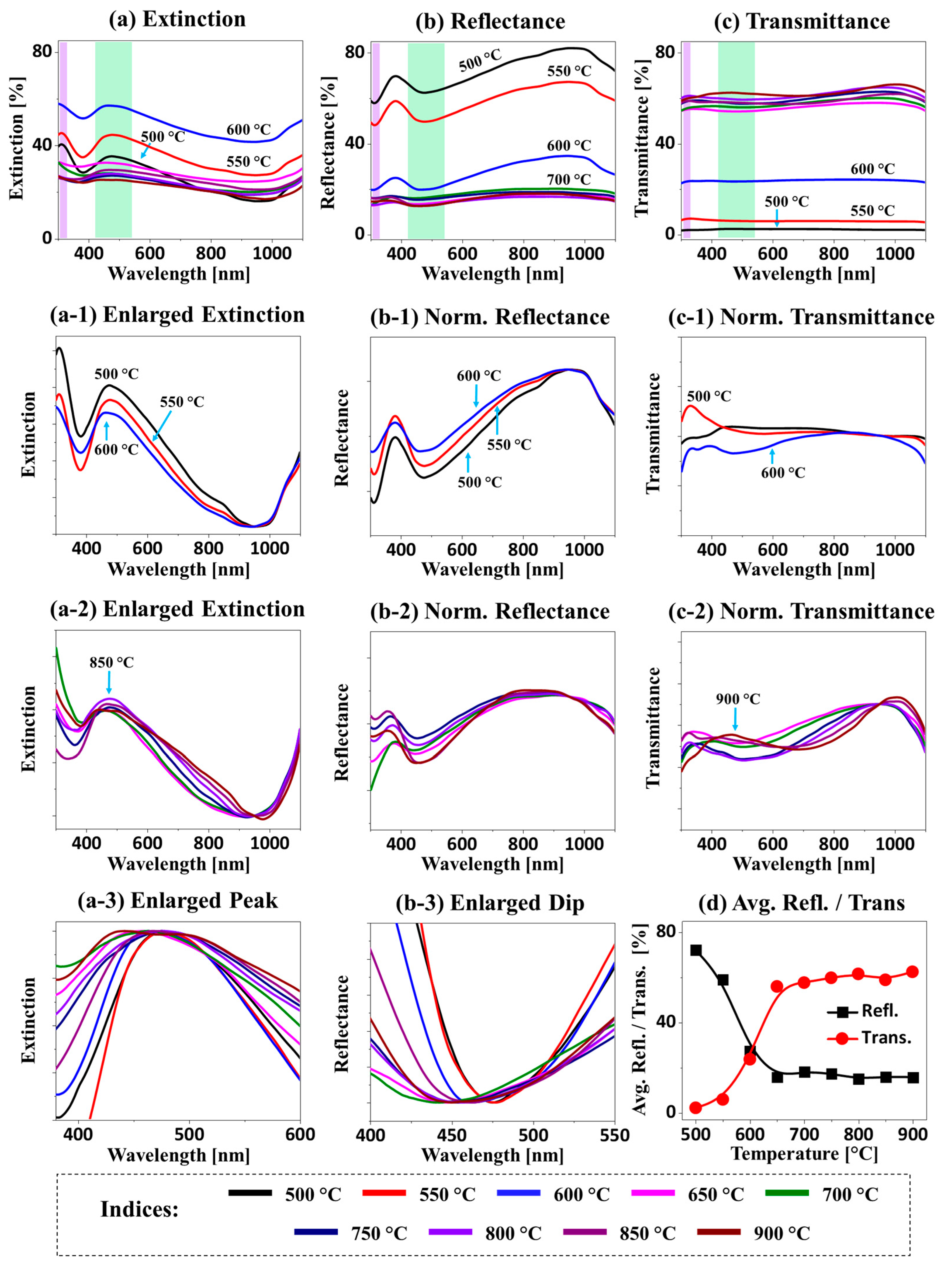
Figure 4 shows the LSPR properties of the Ag–Pt and Pt nanostructures fabricated with Ag
70 nm/Pt
15 nm in terms of extinction, reflectance, and transmittance spectra. In addition, the local e-field enhancement of a typical Ag–Pt and Pt NP is simulated in
Figure 5. The material constants of alloy nanostructures were determined by averaging the pure Ag and Pt on the basis of the atomic percentage (at %) of Ag and Pt, as discussed [
21,
22]. The simulated extinction spectra are provided in
Figure A4. In general, depending upon the structural configuration and elemental composition of the nanostructures, the optical spectra exhibited distinct wavelength-dependent behaviors. First of all, the extinction spectra in
Figure 4a demonstrate two distinctive LSPR bands, including the intense absorption peaks in the UV and VIS region with the Ag–Pt alloy nanoclusters at a temperature below 650 °C, whereas a relatively weaker and broader absorption peak was observed with the Pt NPs above 650 °C. This could have been caused by the desorption of Ag atoms as well as the size reduction of nanoclusters with temperature [
31]. Since the NPs in this set were larger than 400 nm in width and had a wide size distribution, the dipolar, quadrupolar, and other resonance modes could overlap and give rise to a superimposed multipolar resonance mode in the VIS region and a higher-order resonance mode in the UV region [
32]. Thus, the development of an extinction peak in the VIS region at around 500 nm in
Figure 4a could be related to a multipolar resonance mode, and that in the UV region at around 300 nm could be assigned to a higher-order plasmon resonance mode. In a simulation of a typical Ag–Pt alloy nanocluster, as shown in
Figure 5a–c and
Figure A4, multiple extinction maxima appeared in the visible region at around 470, 580, and 750 nm due to the excitation of various plasmonic modes, as discussed. Thus, it can be speculated that Ag–Pt nanoclusters with wide coverage and size distributions could have resulted in the formation of a stronger superimposed LSPR band in the UV-VIS region. In the e-field profiles (shown in
Figure 5b,c), the e-field was stronger at the boundary (or surface) of the NPs. An e-field vector related to the multipolar resonance mode showed multiple directions, as shown in
Figure 5b-1,c-1.
In the case of isolated Pt NPs between 650 and 900 °C, while much reduced absorption bands were observed, the VIS absorption band was slightly increased at a high
Ta, with slightly improved uniformity of Pt NPs, as displayed in
Figure 4a-2. The e-field was very confined at the boundary, and the number of extinction maxima in the visible region were decreased in the case of Pt NPs, as observed in
Figure 5e,f and
Figure A4. On the other hand, the extinction maxima were significantly blue-shifted at around 315 and 500 nm because of the smaller size of the Pt NPs. Similarly, the e-field vectors were also altered, and the number of vector directions was reduced, which could have been correlated with the excitation of less-plasmonic modes with the reduced size and improved uniformity of Pt NPs. Furthermore, the corresponding reflectance spectra are presented in
Figure 4b, and they exhibited a narrow absorption dip in the UV region and a wide absorption dip in the VIS region corresponding to the higher order and multipolar resonance modes of nanostructures, as discussed. For the Ag–Pt alloy nanostructures, the absorption dips were generally strong but were gradually reduced with the desorption of Ag at increased
Ta, as shown in
Figure 4b-1. For the Pt NPs at a high
Ta, the absorption was much reduced and broadened, as shown in
Figure 4b-2. The broadening of the absorption dip in the VIS region (with a low Ag content and Pt NPs) is shown in
Figure 4b-3.
In the transmittance spectra, a sharp distinction between the Ag–Pt alloy and the Pt NPs was observed, as shown in
Figure 4c. In particular, lower transmittance was observed for the lower Ta samples due to the wide surface coverage of the Ag–Pt nanostructures. The normalized transmittance spectra of the Ag–Pt alloy nanostructures in
Figure 4c-1 demonstrated low absorption in the VIS region, likely due to high forward scattering [
33]. With increased
Ta, the absorption dip became smoother (along with the formation of Pt NPs), likely due to the gradual reduction of forward scattering as the size of the NPs was reduced compared to the Ag–Pt NPs. For the Ag–Pt nanostructures, the average reflectance was generally high, while the transmittance was low, as presented in
Figure 4d, due to high surface coverage. The opposite was observed for the Pt NPs due to much-reduced coverage. In short, the Ag–Pt NPs with an Ag component showed much-improved plasmonic properties [
23,
24]. While the Pt NPs in this study showed a much-reduced extinction response compared to the Ag–Pt NPs, these reflectance spectra still demonstrated enhanced plasmonic peaks in the UV and VIS regions compared to the pure Pt NPs in the previous study [
24].
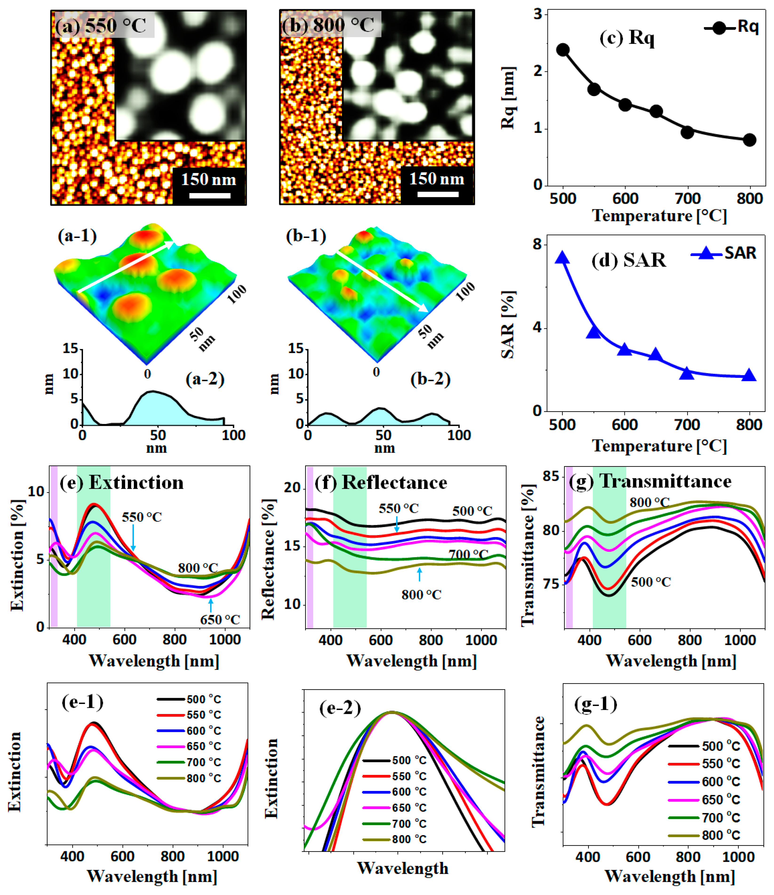
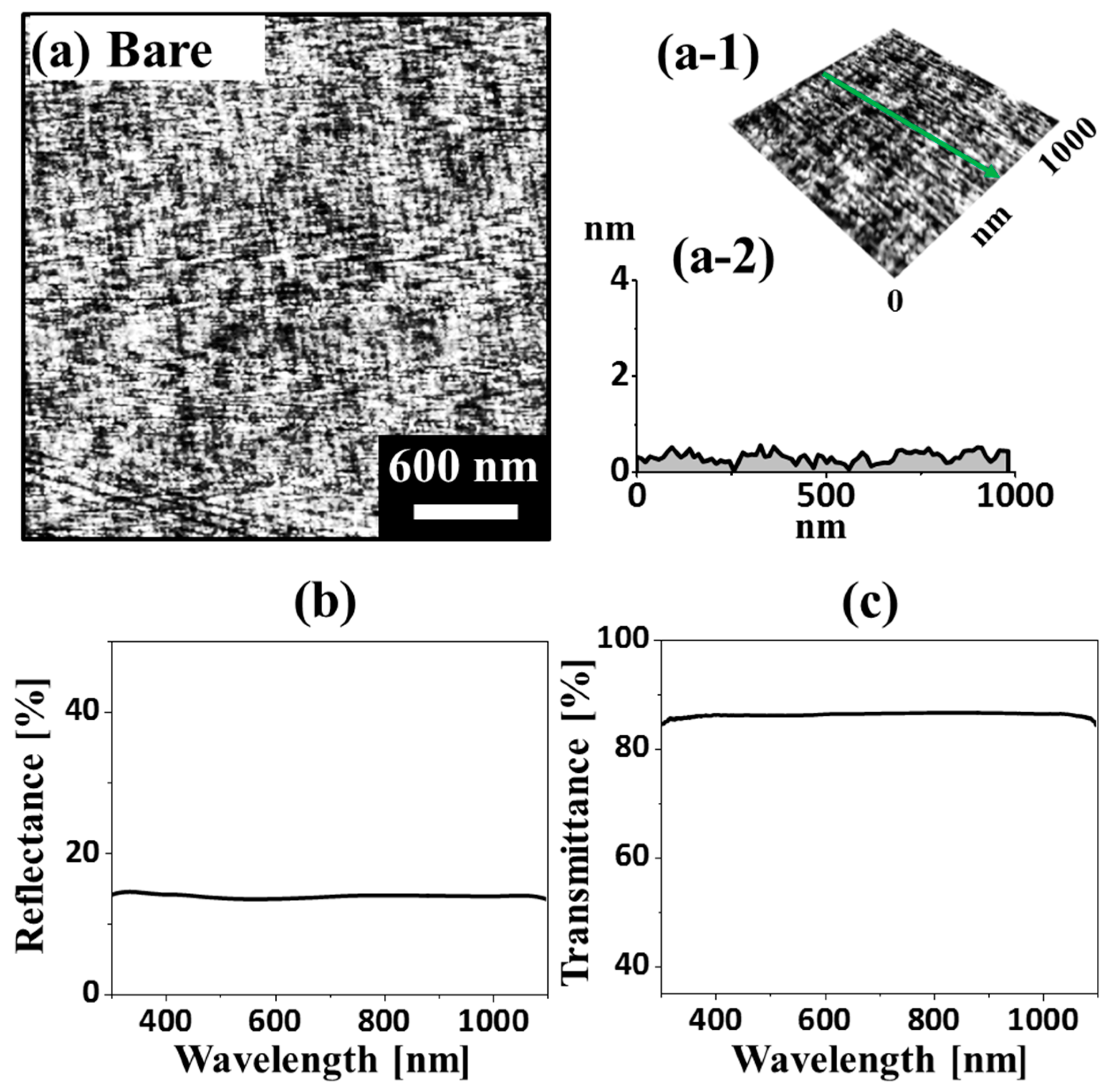
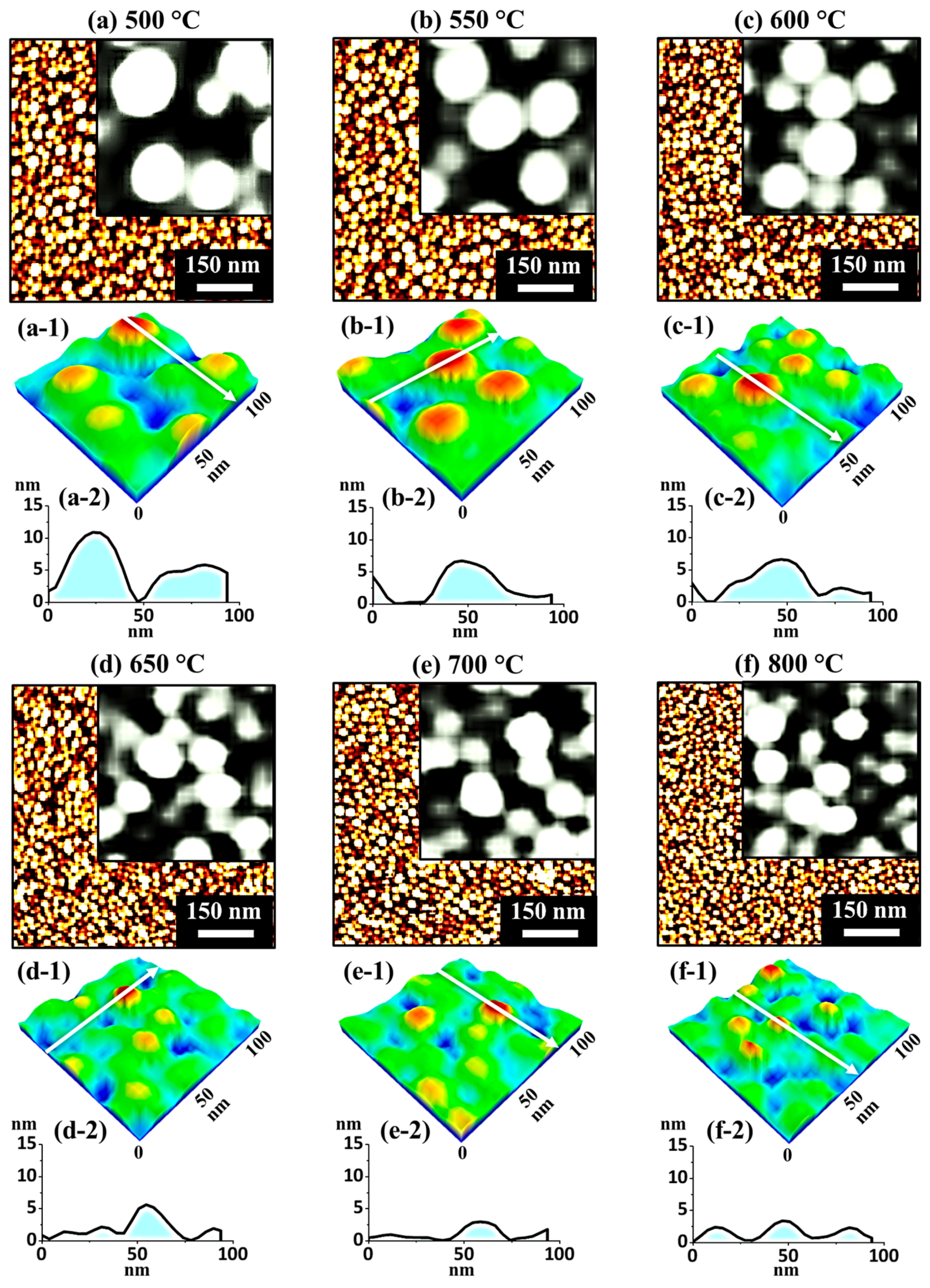
Figure 6 shows the fabrication of tiny Ag–Pt and Pt NPs on sapphire (0001) with the Ag
2.8 nm/Pt
0.6 nm bilayers at 550 and 800 °C. The detailed evolution of NPs at specific
Ta is presented in
Figure A5, along with AFM top-views, side-views, and cross-sectional line profiles. Generally, the dewetting of thin film inversely depends upon the initial film thickness, i.e., the thinner the film, the higher the dewetting rate [
34]. In this set, due to the much thinner thickness of the Ag–Pt bilayer with a high percentage of Ag, the much-enhanced diffusion, alloying, and nucleation of isolated NPs could be achieved at a low
Ta. Thus, the NPs obtained were very small and dense compared to the previous set. For instance, densely packed Ag–Pt alloy NPs 8 nm in height and 40 nm in diameter were formed at 550 °C, as shown by the AFM top-views and color-coded side-views in
Figure 6a,a-1. The corresponding cross-sectional line profile revealed the height of the Ag–Pt NPs, which was nearly 12 times smaller than the previous set in identical conditions. Furthermore, these NPs attained an isolated and round shape even at low
Ta due to enhanced diffusion through the alloying of atoms [
34]. As the
Ta increased, the size of the NPs was reduced, as shown in
Figure 6b, due to the rapid sublimation of the Ag atom. At a
Ta above 600 °C, the Ag atoms were fully desorbed from the NP matrix, and as a result, pure Pt NPs were formed. The average size of the Pt NPs was less than 5 nm in height and 25 nm in diameter, as clearly shown by the cross-sectional line profiles in
Figure 6b-2. Additionally, the overall growth in the NP size is expressed in terms of
Rq and the SAR, as displayed in
Figure 6c,d. As
Ta increased between 500 and 800 °C,
Rq and the SAR gradually decreased due to the reduction in height and surface area of the NPs.
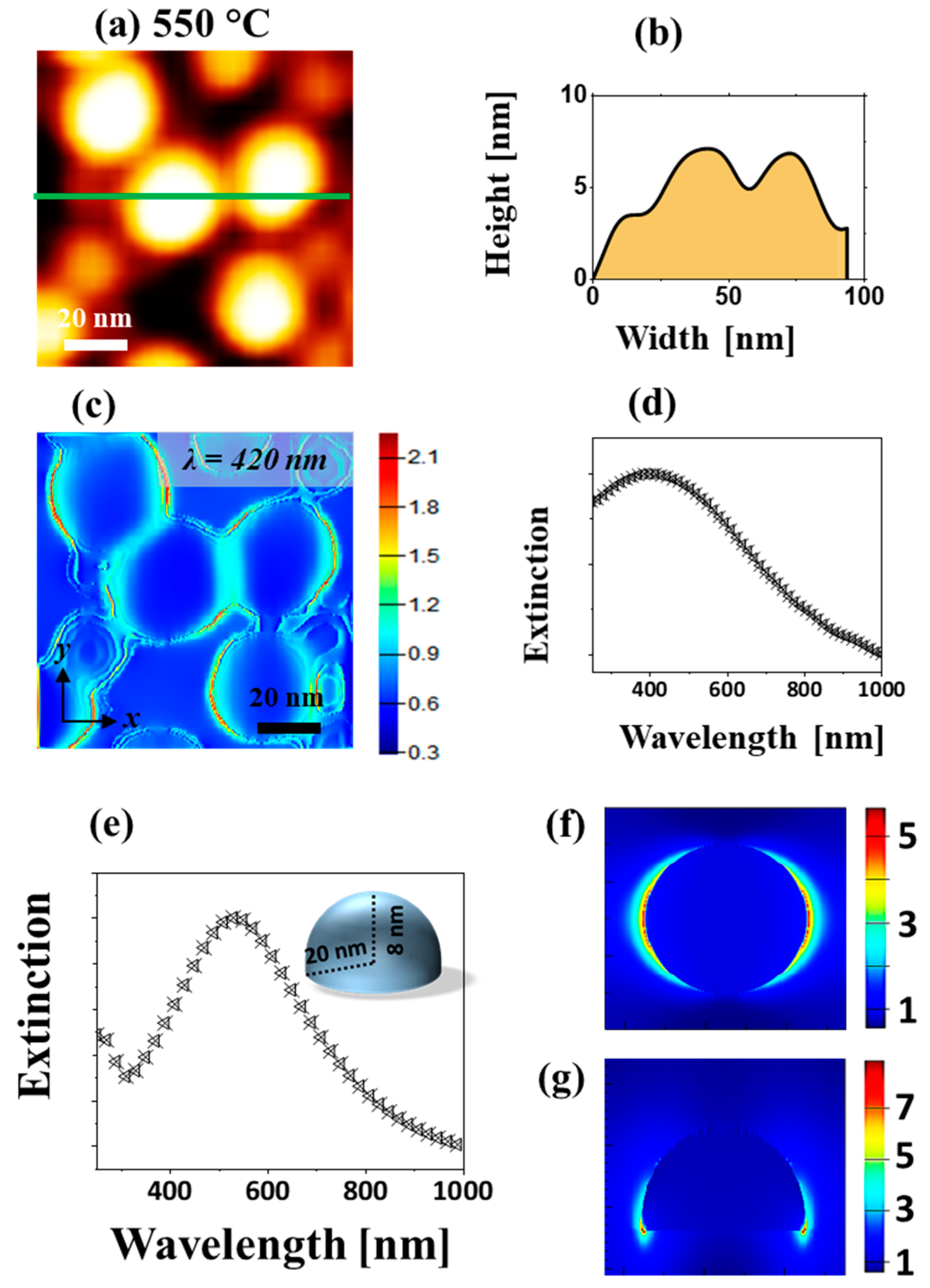
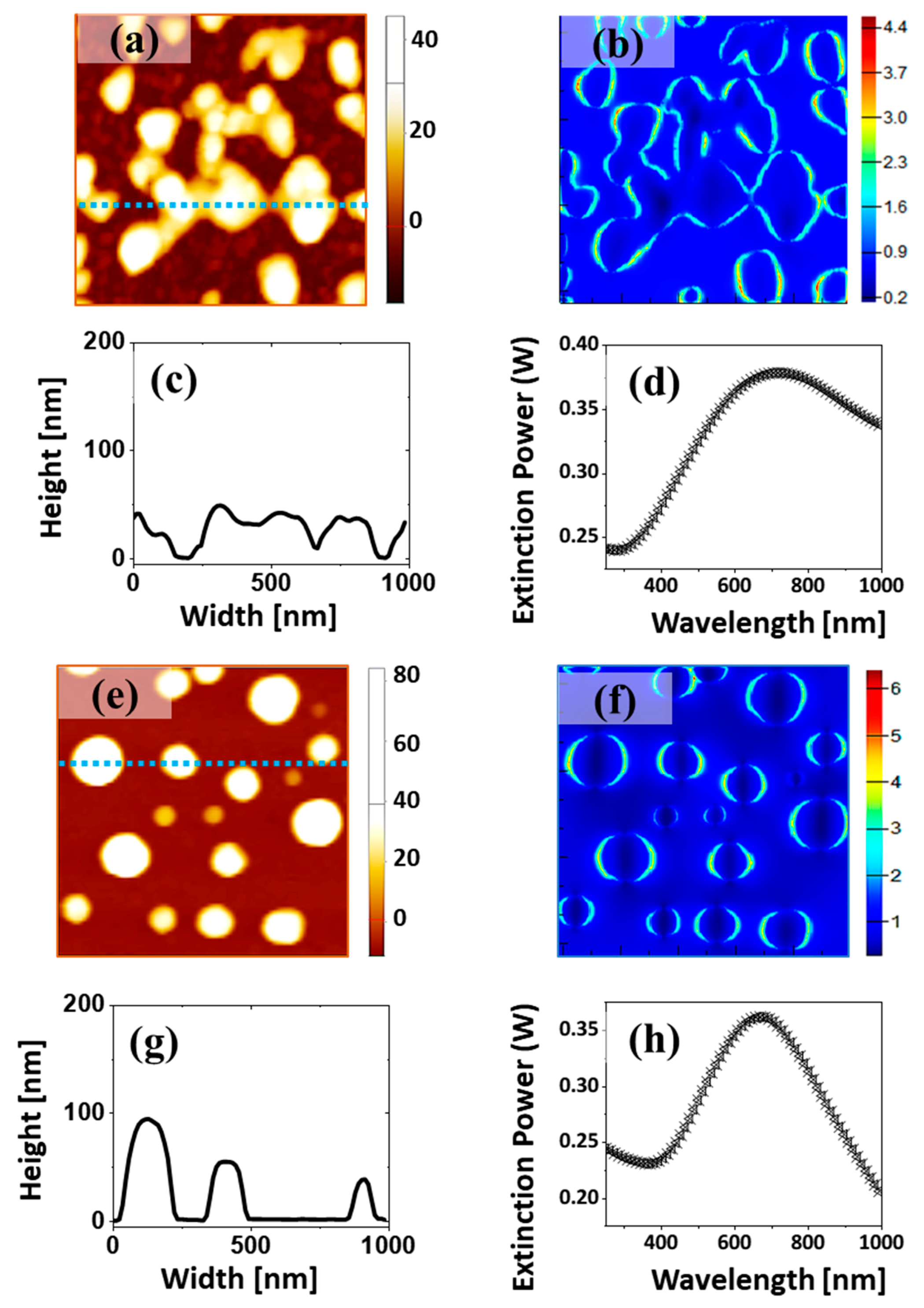
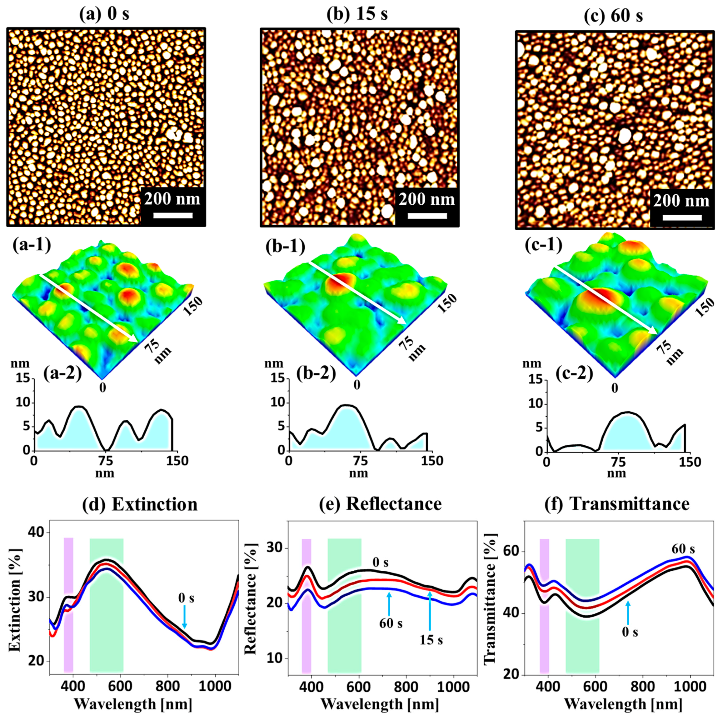
The corresponding optical properties of small and dense Ag–Pt and Pt NPs fabricated with the Ag
2.8 nm/Pt
0.6 nm bilayers are presented in
Figure 6e–g. Based on the distinct size and elemental composition of the NPs, the extinction, reflectance, and transmittance spectra showed distinctive responses from the previous set. In general, the extinction spectra in
Figure 6e,e-1 exhibited a comparatively stronger absorption peak in the VIS region (~490 nm) and a weaker peak in the UV region (~310 nm). As the NP size was much smaller in this set (<12 nm in height and <50 nm in diameter), the corresponding two extinction peaks could be assigned to the quadrupolar resonance mode at ~310 nm and the dipolar resonance mode at ~490 nm [
34]. The localized e-field distribution on a typical Ag–Pt NP was simulated, as shown in
Figure 7. First, the simulation was performed with an imported typical AFM image using the model explained in the experimental section. As shown in
Figure 7c,d, a dipolar plasmonic mode was observed, with extinction maxima at ~420 nm. The simulated extinction peak was blue-shifted compared to the experimental one, which could have been due to the disparity in size between the AFM image and real NPs. In addition, an ideal semi-ellipsoid 40 nm in diameter and 8 nm in height corresponding to the average size and dimension of the Ag–Pt NPs was simulated using a periodic boundary condition in the
x,
y directions with 80 nm of periodicity, as shown in
Figure 7e,f. A dipolar resonance mode was observed at ~520 nm, which showed a strong e-field confinement on the surface of the NPs, as shown in
Figure 7f,g. Furthermore, a quadrupolar shoulder was observed in the UV region, as seen in
Figure 7e. The simulated and experimental extinction spectra generally agreed well, although the resonance peak positions were somewhat deviated, likely due to the difference in real and simulated NPs.
In comparison to the previous set, the overall absorption was largely reduced in this set due to the much smaller size of the NPs with a lower Ag content. The extinction spectra were normalized in order to show the morphology and composition-dependent plasmonic responses in
Figure 6e-1. Specifically, with Ag–Pt alloy NPs at 500 and 550 °C, the absorption peaks were relatively stronger due to the presence of Ag content and the relatively larger size of the NPs, as clearly shown by the strong dipolar resonance peaks. As the Ag atoms were gradually sublimated, relatively smaller Pt NPs were formed, and the intensity of the dipolar resonance peak was gradually reduced between 600 and 800 °C. Furthermore, the dipolar resonance peak showed a gradual broadening at higher
Ta, as shown in
Figure 6e-2 with the NP evolution. These dipolar resonance peaks were significantly narrower and had shorter wavelengths than the large NPs in the previous set due to much smaller sizes and improved uniformity [
32]. Furthermore, the corresponding reflectance spectra of the small-sized Ag–Pt alloy and the Pt NPs are presented in
Figure 6f. Generally, an absorption dip could be expected in the VIS region instead of the shoulder; however, a shoulder was observed in the UV-VIS region due to enhanced backward scattering with small NPs [
31]. The corresponding transmittance spectra in
Figure 6g reveal a narrow absorption dip in the UV region (~310 nm) and a wide absorption dip in the VIS region (~490 nm) corresponding to quadrupolar and dipolar resonance modes, as discussed [
33]. The absorption was gradually reduced with a higher
Ta along with decreased NP size and Ag sublimation, as shown in
Figure 6g-1. Likewise, the absorption dip gradually widened with the formation of smaller Pt NPs at increased
Ta. In contrast to the previous set, this set revealed much narrower absorption dips in the VIS region due to the formation of much smaller and uniform NPs [
32].
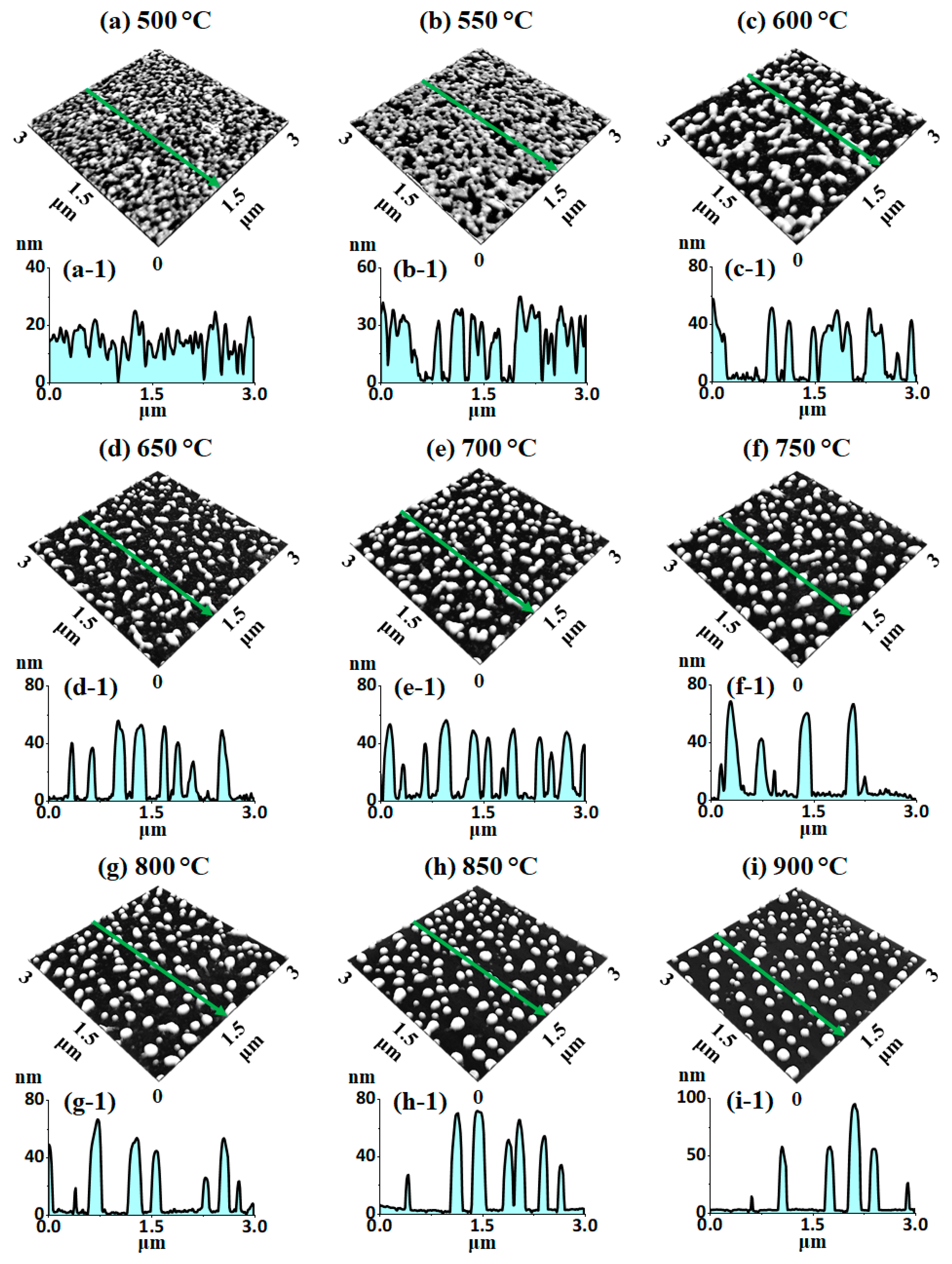
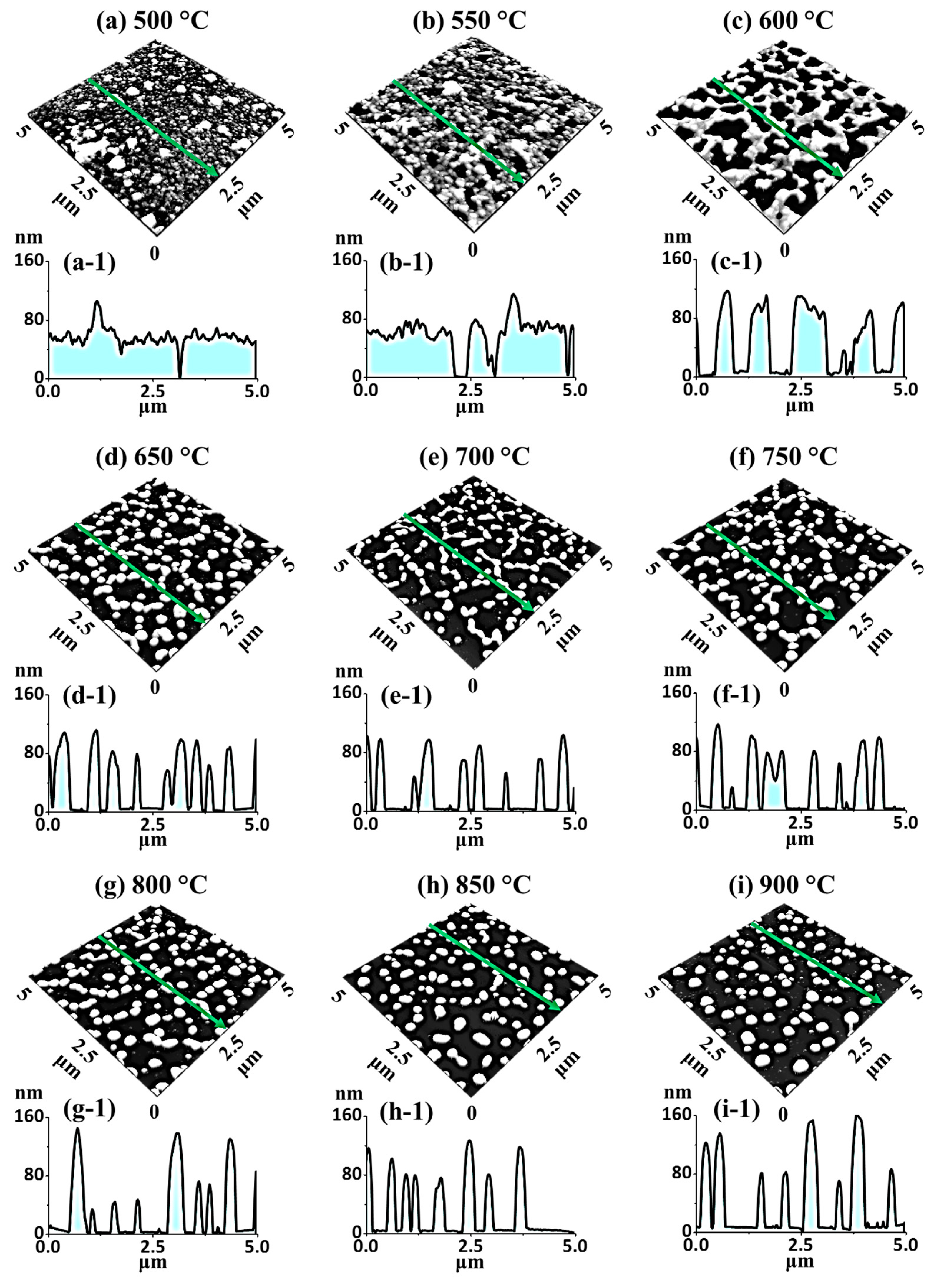
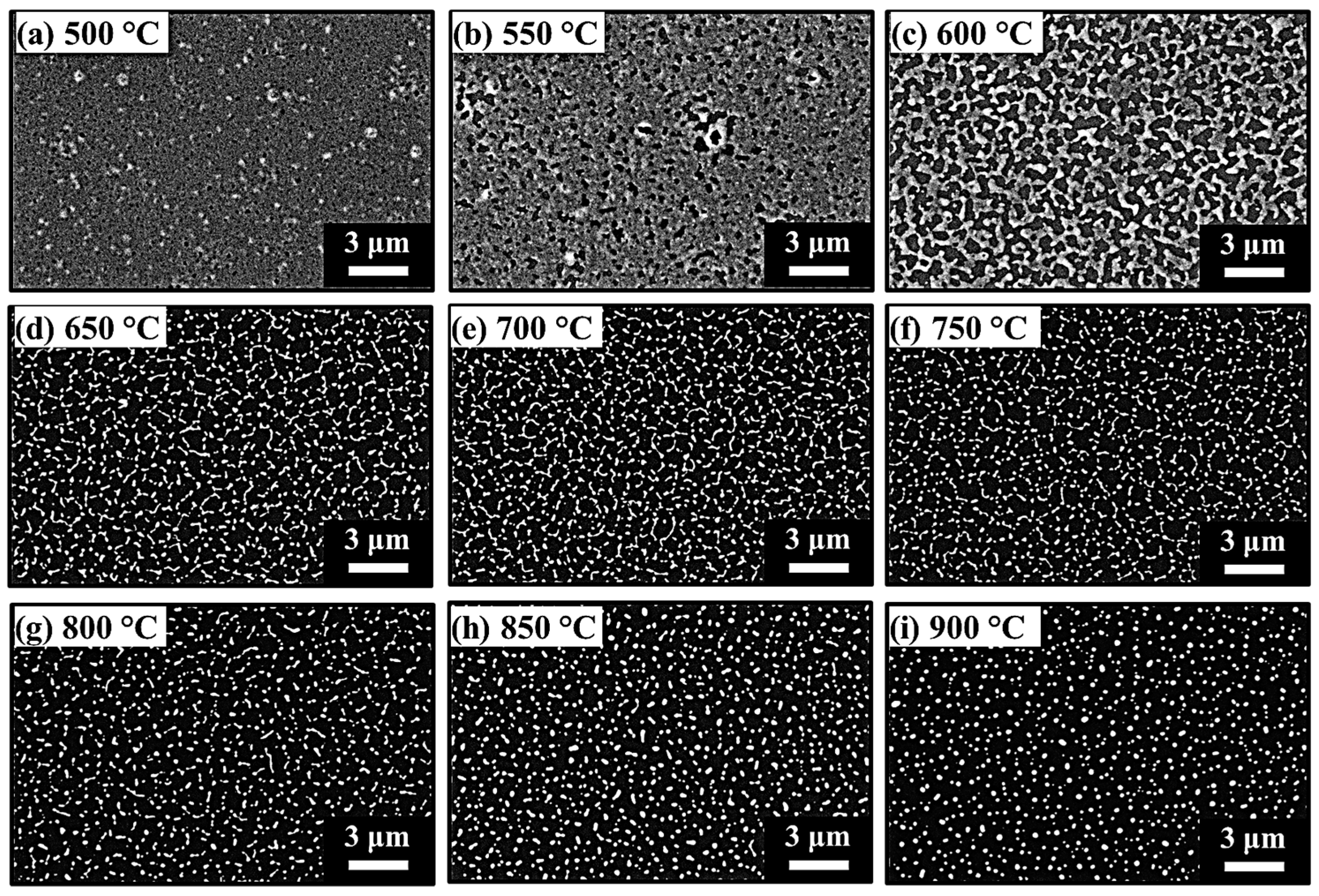
Figure 8 shows the gradual evolution of medium-sized Ag–Pt and Pt NPs from the Ag
15 nm/Pt
7.5 nm bilayers on sapphire (0001) through annealing between 500 and 900 °C for 120 s. This set of samples was prepared to realize medium-sized NPs under identical growth conditions. In general, the nanostructures were gradually evolved from interconnected and irregular to well-isolated semispherical configurations along with increased
Ta. When comparing them to previous sets, these NPs were at the intermediate stage in size and density, as final size and configuration directly depended on the initial bilayer thickness, as discussed. In fact, the total deposition thickness as well as individual thickness of the bilayer was largely reduced compared to the first set. Therefore, the dewetting could occur much faster and at a relatively lower
Ta [
34]. Specifically, the annealing of the Ag
15 nm/Pt
7.5 bilayer at 500 °C developed numerous voids and connected nanostructures, as shown in
Figure 8a,a-1. Compared to the first set at the same
Ta, the voids were much smaller and denser due to the rapid nucleation of the thinner Ag–Pt bilayer. The voids were ~22 nm in depth and 70 nm in width, as clearly seen in the line profile in
Figure 8a-2. Consequently, the evolution of the irregular Ag–Pt nanocluster was observed at 600 °C, which could be correlated with the coalescent growth of voids in order to minimize the interface energy, as discussed [
27,
28].
Meanwhile, the large nanoclusters started to fragment, likely due to Rayleigh-like instability, and the corresponding line profile showed increased average vertical height of the nanostructures, while the lateral width was sharply decreased. The FFT power spectra were gradually reduced in size, as presented in the insets of the AFM top-views, which could be correlated with decreased height distribution along with the evolution of Ag–Pt nanoclusters. In addition,
Rq and the SAR were sharply increased between 500 and 600 °C due to the increased height of the nanostructures and surface area exerted by the nanostructures, as shown in
Figure 8g. Similarly to the previous sets, well-developed pure Pt NPs were obtained above 650 °C due to Ag sublimation, as shown in
Figure 8d–f. The corresponding EDS counts and spectra are shown in
Figure 8h,i, which exhibit nearly consistent Pt peak counts, indicating no desorption of Pt atoms regardless of the variant surface morphology with increased
Ta. However, in the case of Ag peaks, the counts were sharply decreased between 500 and 600 °C and became equal to the background at higher
Ta, as shown in
Figure 8h. In addition, a detailed elemental analysis is presented in
Figure 9. For a typical nanocluster fabricated at 550 °C, the SEM image matched well with the Ag and Pt phase maps, as shown in
Figure 9a–d. Similarly, the EDS line profile through the nanoclusters revealed the similar intensity of Ag Kα1 and Pt Mα1. From the results, it was clear that the Ag and Pt atoms were well intermixed in the nanoclusters during the dewetting process.
Along with Ag sublimation, the large nanoclusters were further fragmented, resulting in smaller NPs at 650 °C. At this stage, the lateral size of nanostructures was extensively decreased, whereas the vertical height of the nanostructures remained almost similar, as clearly shown by the AFM images and cross-sectional line profiles in
Figure 8d–d-2. After increasing the
Ta further, i.e., up to 900 °C, the evolution of isolated NPs occurred mildly, as observed in
Figure 8e,f. In the high-
Ta regime, the elongated shape of NPs gradually became semispherical with improved uniformity and spacing, which is also shown by the reduced FFT patterns.
Rq and SAR summary plots of the isolated NPs also showed minor increments with temperature. In this set, the shape, spacing, and size uniformity of the NPs were much improved compared to the pure Pt dewetting due to the concurrent influence of alloying and sublimation [
24]. The evolution of pure Pt NPs at high
Ta was further confirmed by the elemental analysis of NPs at 900 °C, as shown in
Figure 9g–l. The elemental phase maps and EDS line profile clearly show the presence of only Pt in the NP region.
The LSPR properties of medium-sized Ag–Pt and Pt NPs fabricated with the Ag
15 nm/Pt
7.5 nm bilayers are summarized in
Figure 10, and the e-field profile of typical NPs is shown in
Figure A8. First of all, the extinction spectra demonstrated two different spectral shapes, as presented in
Figure 10a–a-3: i.e., the Ag–Pt between 500 and 600 °C and Pt NPs above 650 °C, which again could have been due to Ag sublimation and size reduction. The absorption peaks were gradually attenuated along with the increased
Ta between 500 and 900 °C, as shown in
Figure 10a–a-3. Since the Ag–Pt nanoclusters were generally bigger than 300 nm in this set, the extinction peaks in the UV (~300 nm) and VIS regions (~500 nm) could be assigned to the excitation of higher-order and multipolar resonance modes, respectively [
35]. The simulated e-field and extinction spectra of typical Ag–Pt and Pt NPs are shown in
Figure A8, which exhibits the strong e-field confinement at the boundary of the NPs in both cases. Strong multipolar resonance peaks were observed in the VIS region for large-sized Ag–Pt and Pt NPs. However, extinction peaks were observed at a slightly longer wavelength in the simulated spectra compared to the measured one. In this set, the VIS resonance peak normally had less intensity compared to the first set, which could have been due to the smaller average size and reduced Ag amount. The width of the multipolar resonance peak was found to be narrowed, as presented in
Figure 10a-3, along with the improvement of NP uniformity [
32]. For the isolated Pt NPs between 650 and 900 °C, the intensity of the multipolar peak was slightly enhanced, as shown in
Figure 10a-2, as the average size of the Pt NPs increased due to enhanced atomic diffusion. Likewise, the e-field of the Pt NPs was also enhanced, and the extinction peak was narrowed, as seen in
Figure A8e–h.
In terms of the reflectance spectra presented in
Figure 10b–b-2, the absorption dip of Ag–Pt nanoclusters was gradually reduced with the increased
Ta between 500 and 600 °C due to Ag sublimation. Consequently, the absorption dip completely vanished, and a shoulder was formed in the UV-VIS region, with the isolated Pt NPs between 650 and 900 °C, which could have been due to the strong backscattering of Pt NPs. This further indicated the development of stronger dipolar resonance along with the smaller size of NPs. The transmittance spectra generally revealed a flat response with the Ag–Pt NPs and VIS dip with the Pt NPs (
Figure 10c). Since the Ag–Pt nanoclusters were generally large, the high forward scattering could cause a flat spectral response in the transmittance spectra. However, it was also observed that the absorption dip started to develop at ~500 nm, as shown in
Figure 10c-1, along with the evolution of isolated and relatively smaller-sized NPs. In the case of relatively smaller Pt NPs, they generally showed absorption dips at ~520 nm, as presented in
Figure 10c-2, which could have been due to the shifting of the resonance mode from quadrupolar to dipolar. As the uniformity of the Pt NPs improved between 650 and 900 °C, the absorption dip was enhanced and became narrower, as seen in
Figure 10c-3. In the case of average reflectance and transmittance, they showed an opposite trend (along with the surface coverage change of NPs) (
Figure 10d).


