Evolution of Ternary AuAgPd Nanoparticles by the Control of Temperature, Thickness, and Tri-Layer


Abstract
1. Introduction
2. Materials and Methods
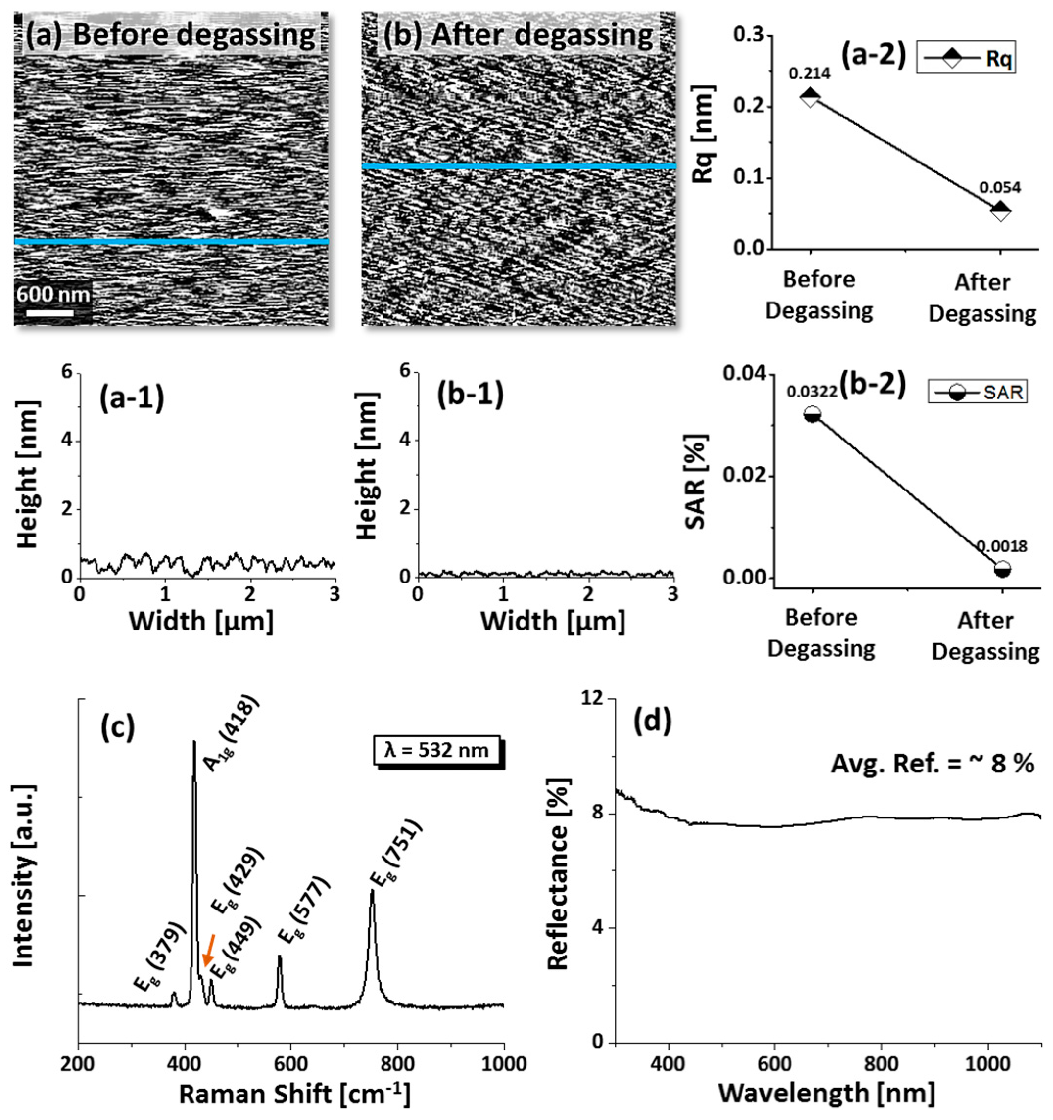
2.1. Substrate Preparation and Fabrication
2.2. Characterization
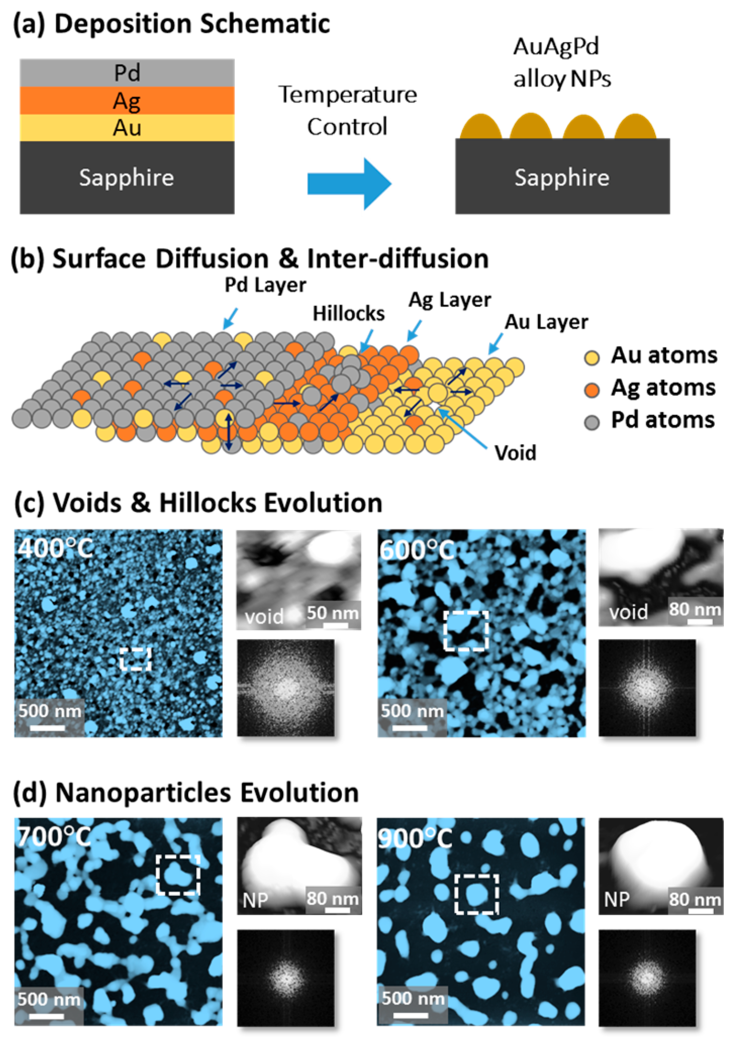
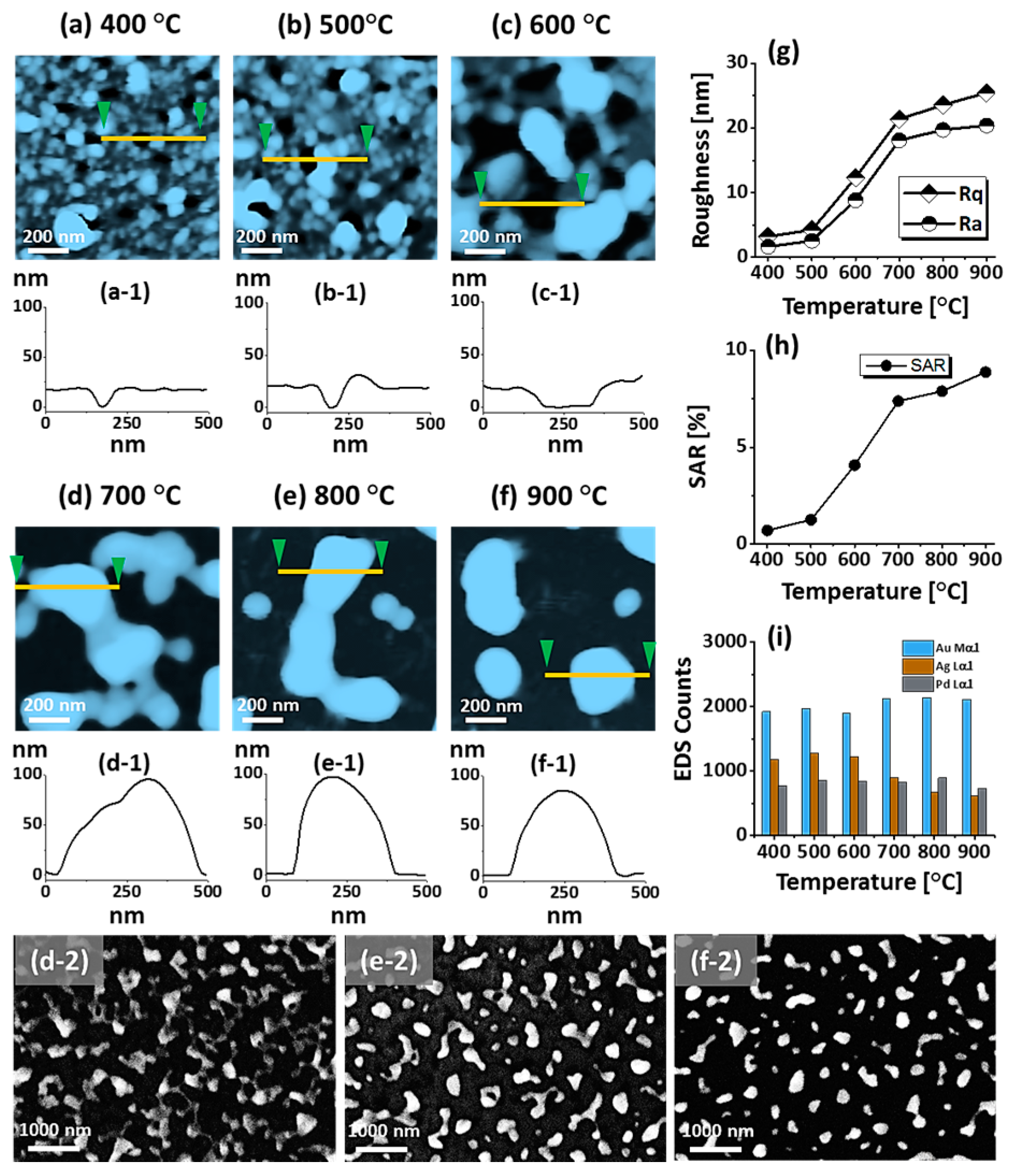
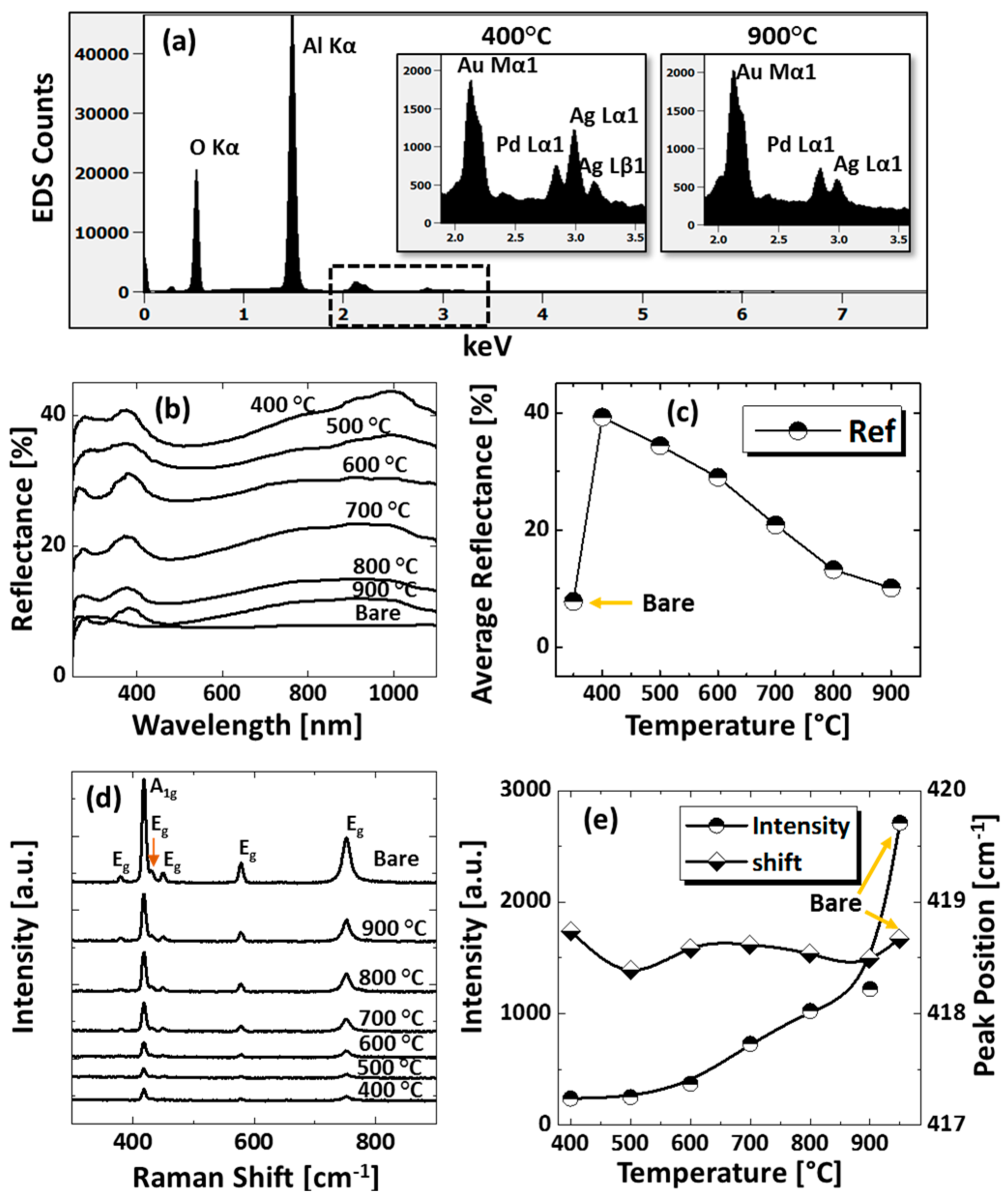
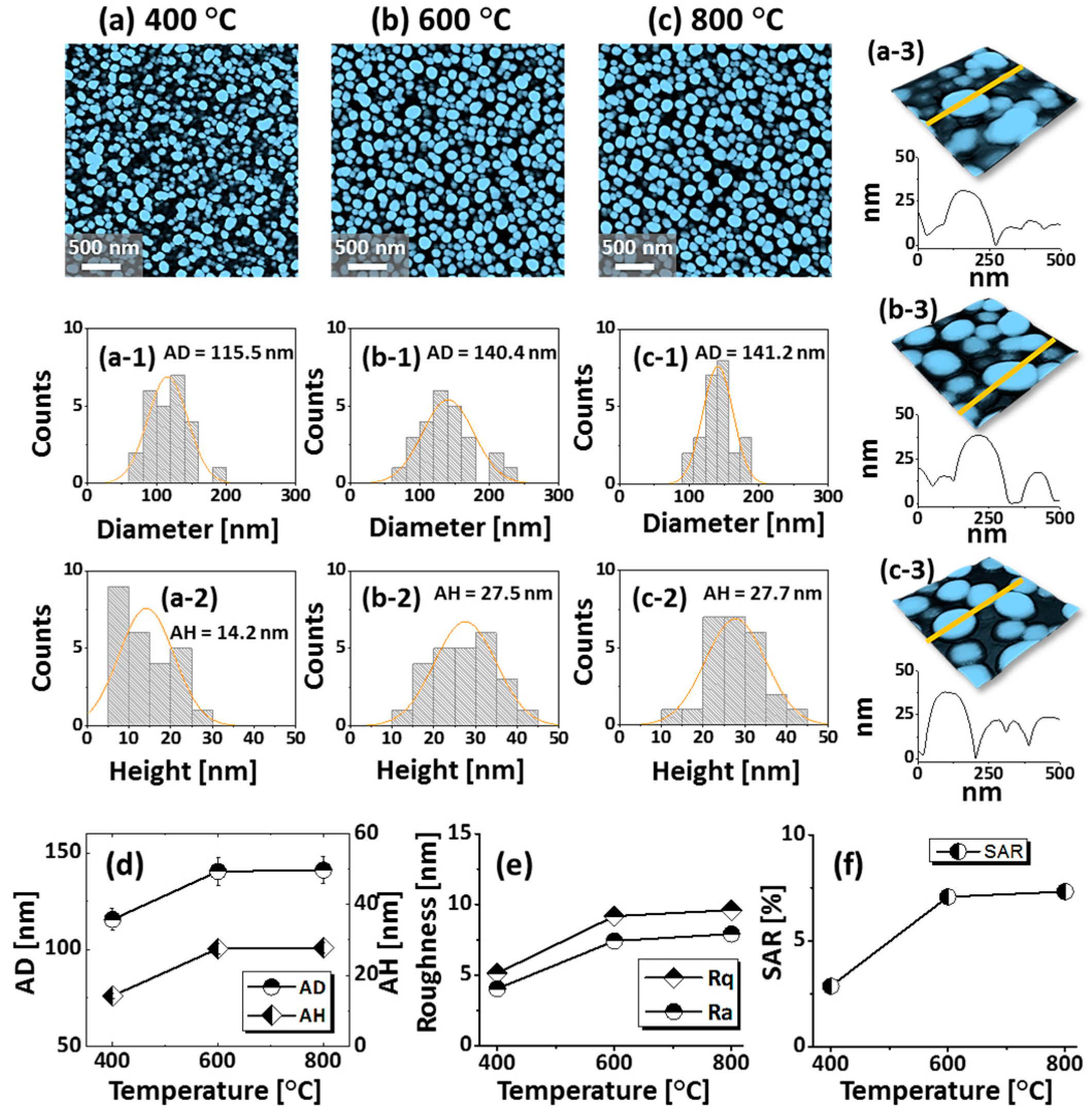
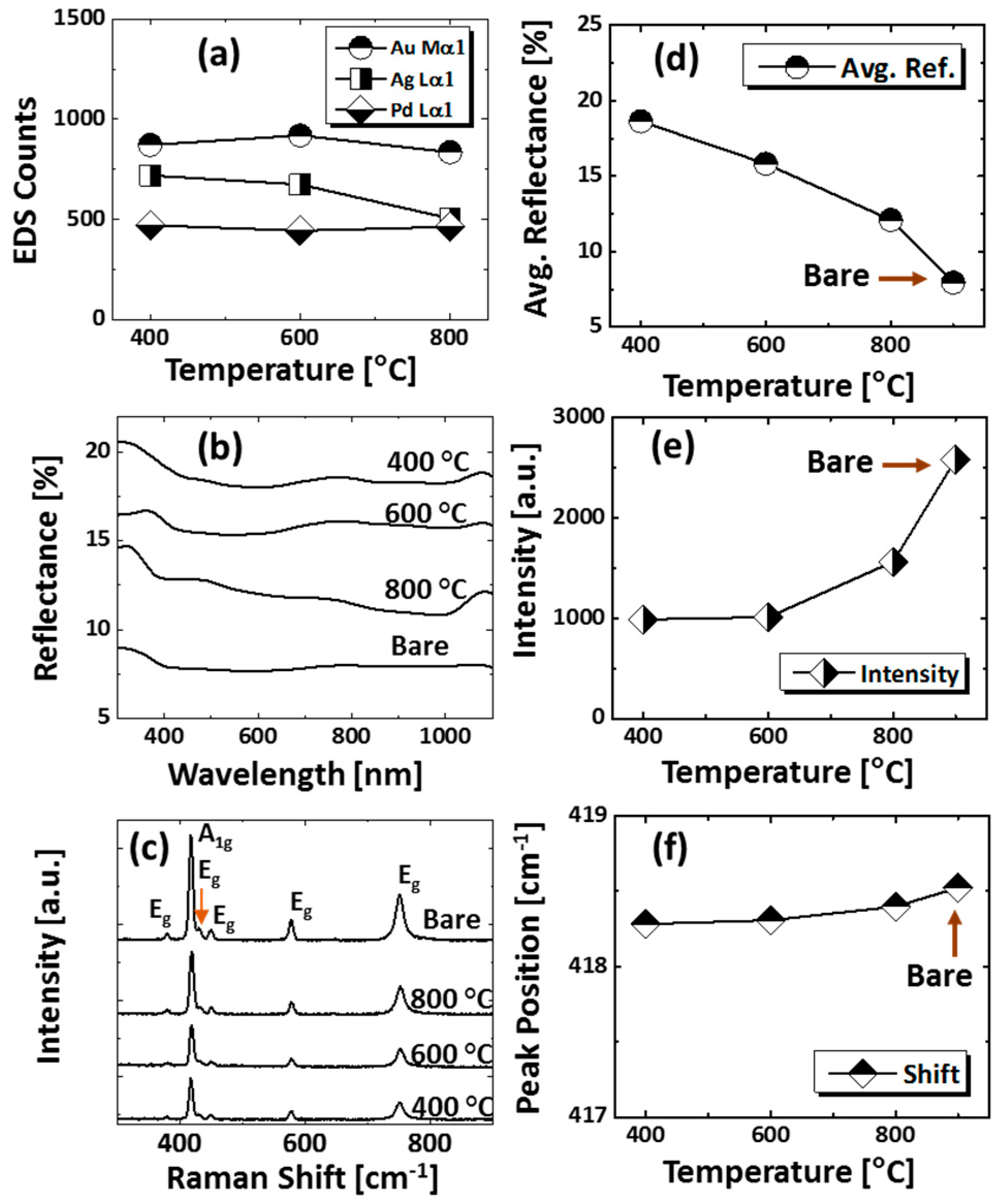
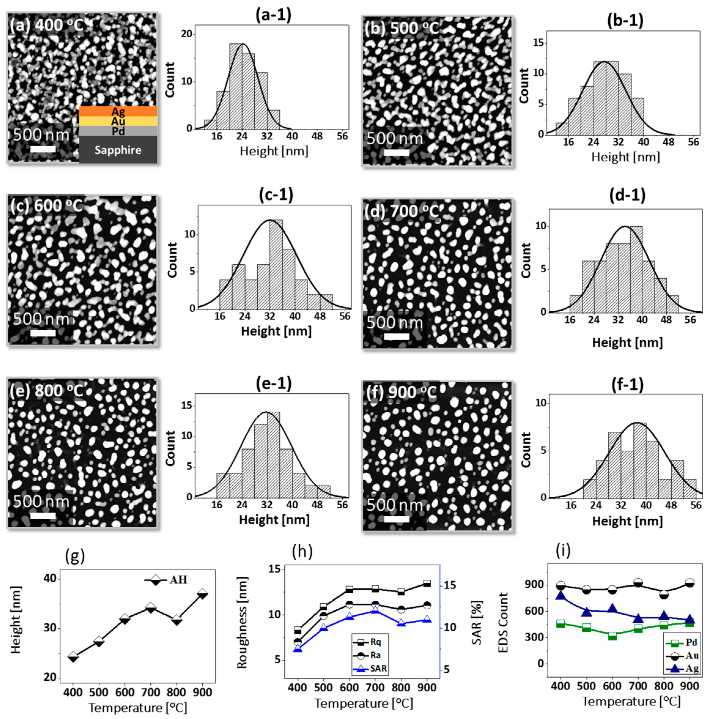
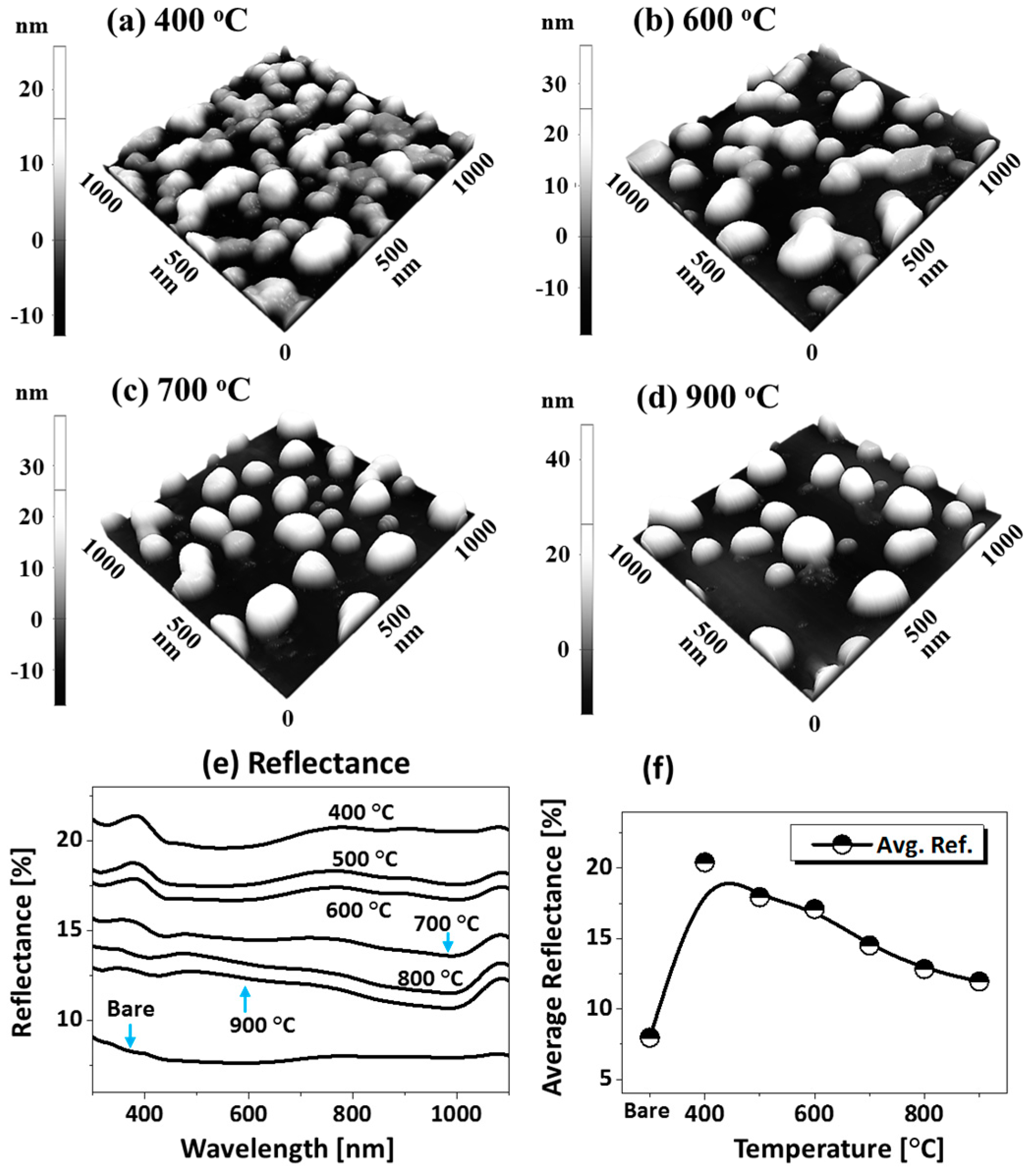
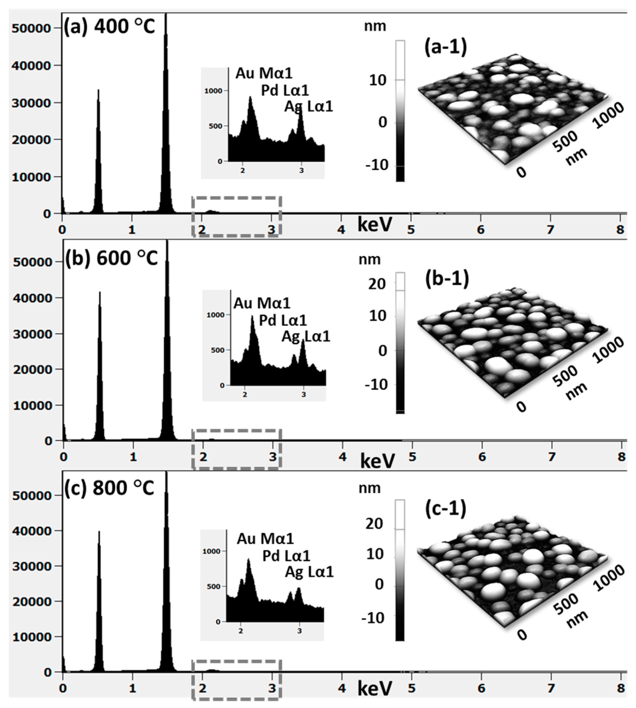
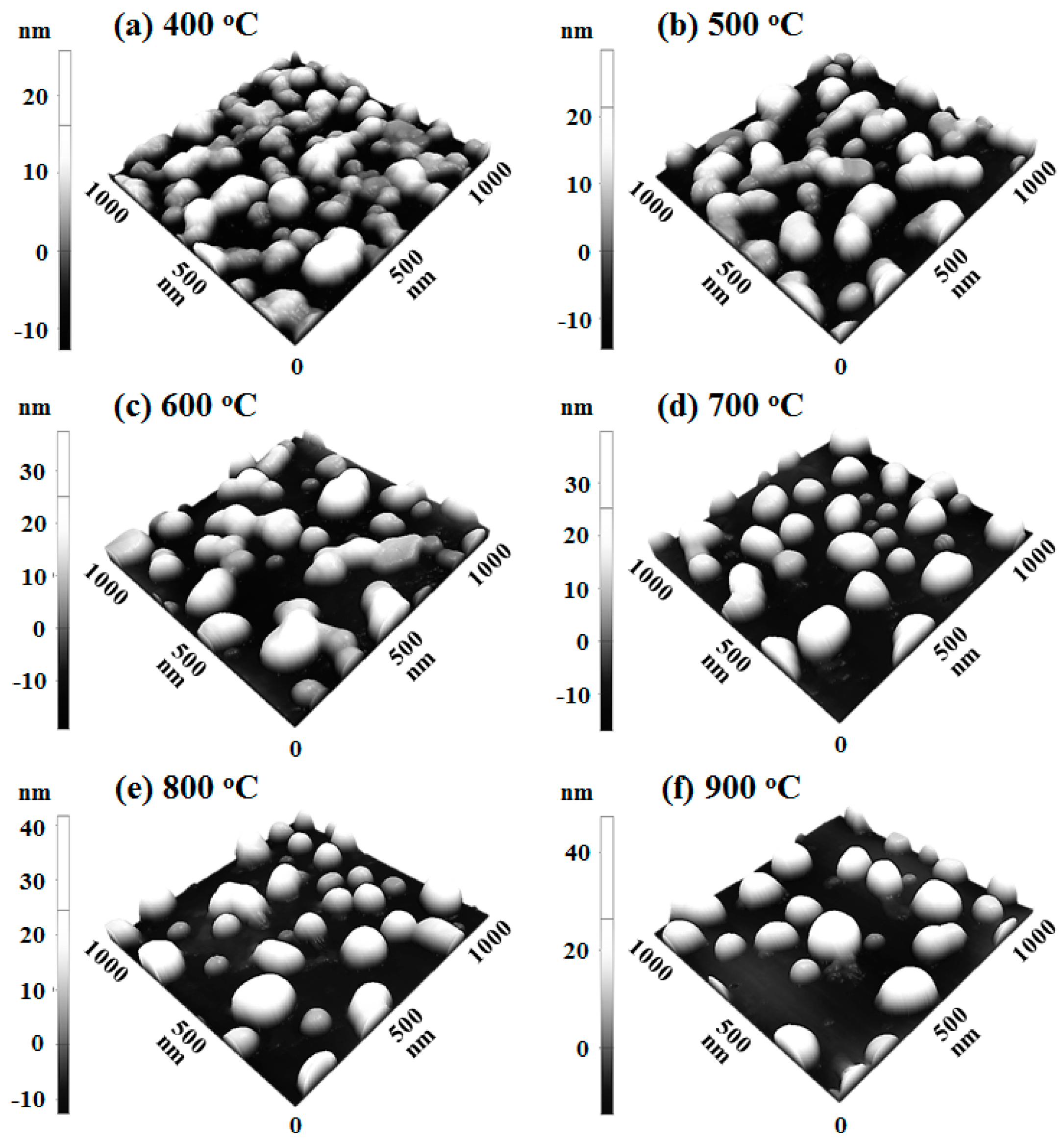
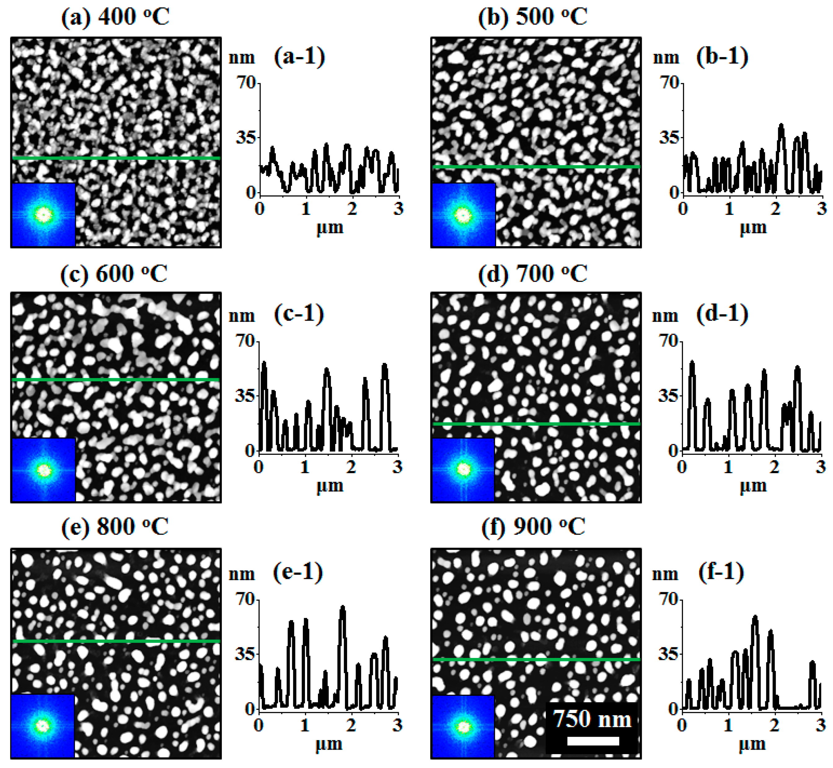
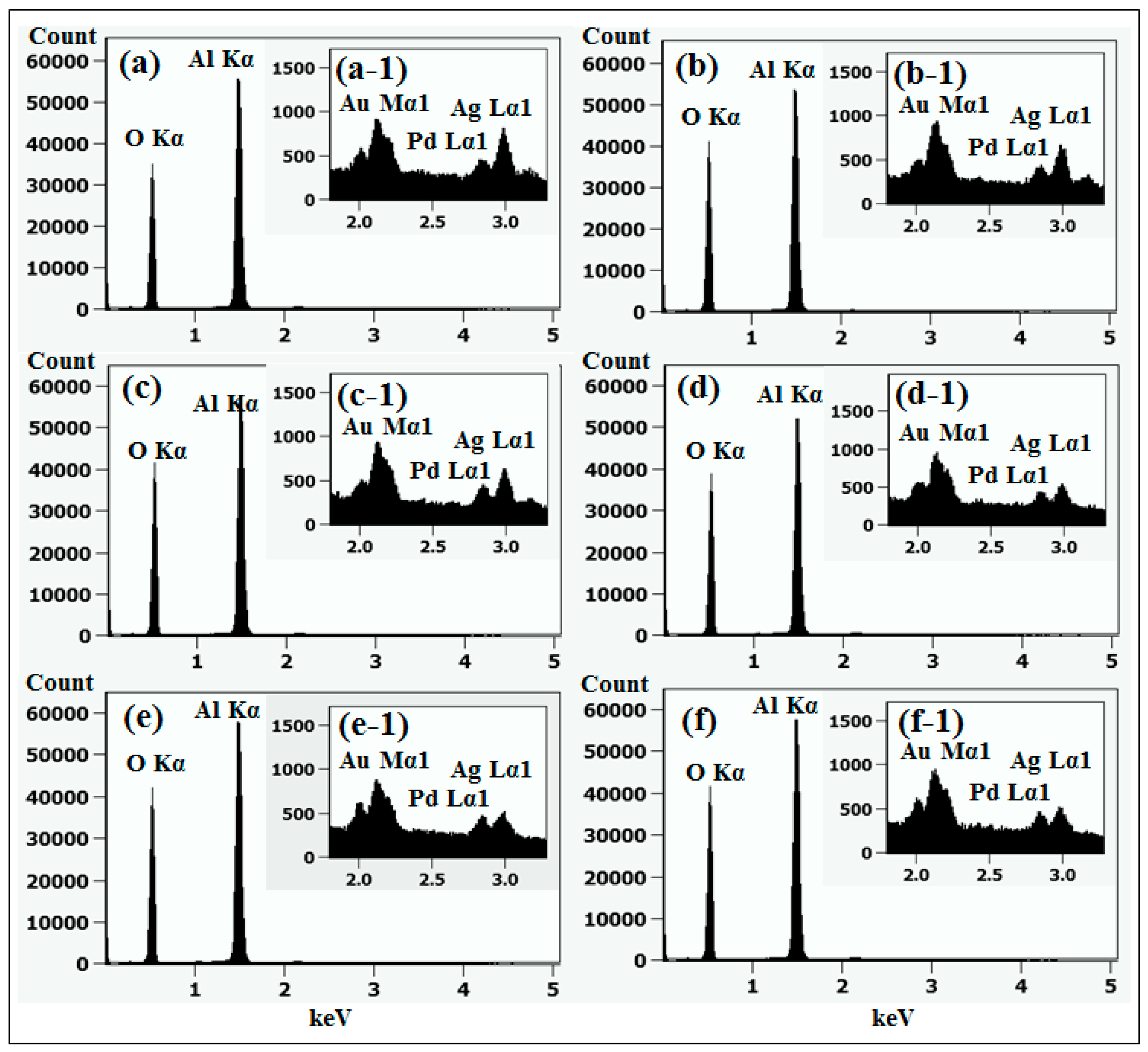
3. Results and Discussion
4. Conclusions
Acknowledgments
Author Contributions
Conflicts of Interest
Appendix A


| Temperature [°C] | Au:Ag:Pd, 15 nm | Au:Ag:Pd, 6 nm | Pd:Au:Ag, 6 nm | |||
|---|---|---|---|---|---|---|
| Rq [nm] | SAR [%] | Rq [nm] | SAR [%] | Rq [nm] | SAR [%] | |
| 400 | 3.18 | 0.7 | 5.13 | 2.86 | 8.32 | 7.5 |
| 500 | 4.12 | 1.25 | - | - | 10.9 | 9.98 |
| 600 | 12.32 | 4.07 | 9.17 | 7.07 | 12.82 | 11.31 |
| 700 | 21.36 | 7.38 | - | - | 12.85 | 12.04 |
| 800 | 23.58 | 7.89 | 9.6 | 7.32 | 12.53 | 10.53 |
| 900 | 25.46 | 8.88 | - | - | 13.47 | 10.98 |
| Temperature [°C] | Au:Ag:Pd, 15 nm | Au:Ag:Pd, 6 nm | Pd:Au:Ag, 6 nm |
|---|---|---|---|
| Ref. [%] | Ref. [%] | Ref. [%] | |
| Bare | 7.821 | 7.951 | 7.96 |
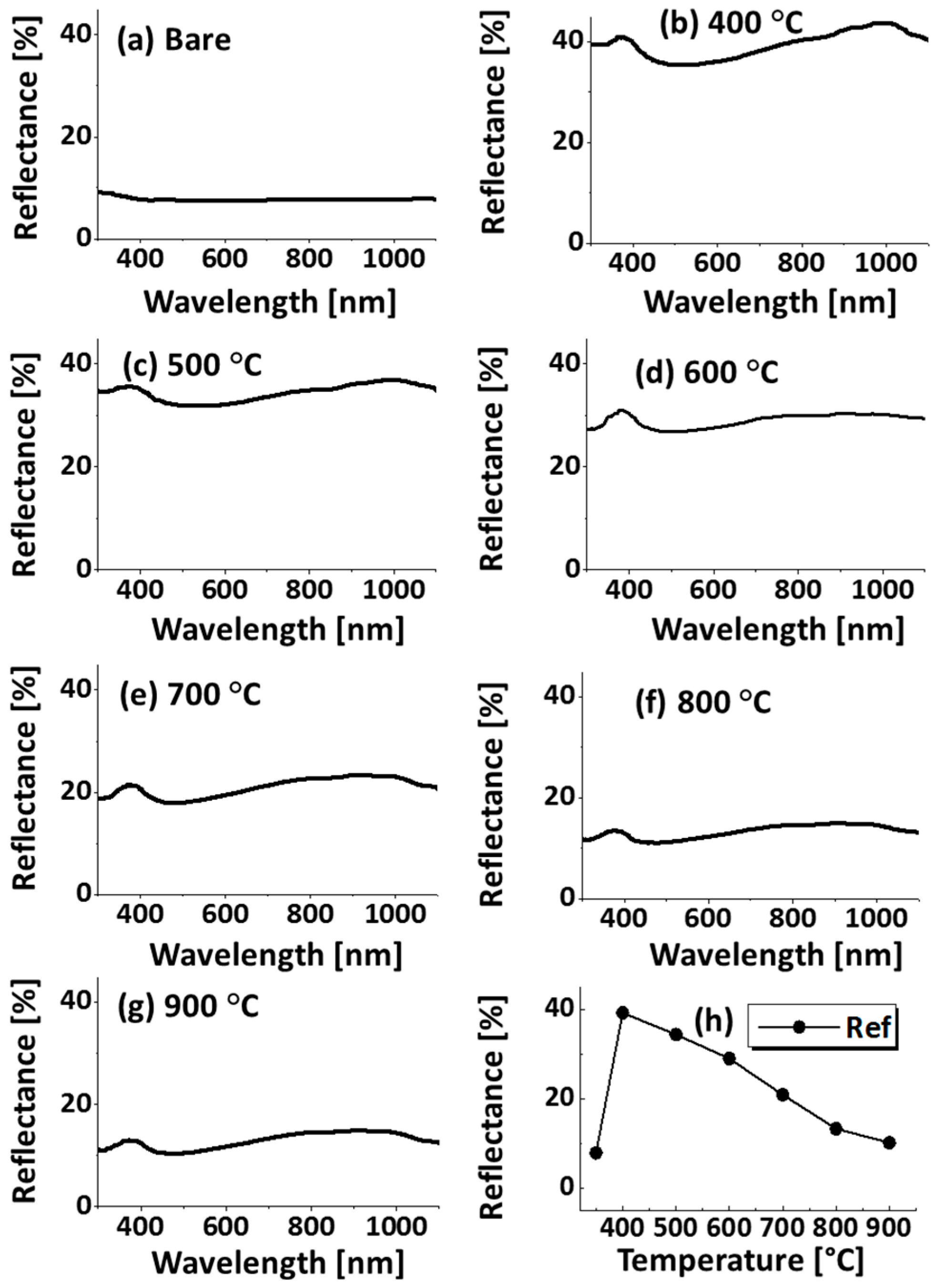
| 400 | 39.258 | 18.629 | 20.41 |
| 500 | 34.385 | - | 17.93 |
| 600 | 29.00 | 15.82 | 17.09 |
| 700 | 20.870 | - | 14.50 |
| 800 | 13.246 | 12.105 | 12.83 |
| 900 | 10.119 | - | 11.94 |
| Temperature [°C] | Au:Ag:Pd, 15 nm | Au:Ag:Pd, 6 nm | Pd:Au:Ag, 6 nm | |||
|---|---|---|---|---|---|---|
| Intensity [a.u.] | PP [cm−1] | Intensity [a.u.] | PP [cm−1] | Intensity [a.u.] | PP [cm−1] | |
| Bare | 2711.73 | 418.67 | 2583.28 | 418.52 | 2786.12 | 417.91 |
| 400 | 238.90 | 418.73 | 987.04 | 418.28 | 972.05 | 417.73 |
| 500 | 251.80 | 418.39 | - | - | 1091.37 | 417.77 |
| 600 | 370.67 | 418.58 | 1011.01 | 418.31 | 1104.38 | 417.71 |
| 700 | 729.88 | 418.62 | - | - | 1348.80 | 417.77 |
| 800 | 1024.83 | 418.54 | 1561.28 | 418.39 | 1510.26 | 417.72 |
| 900 | 1220.36 | 418.49 | - | - | 1511.32 | 417.68 |
| Temperature [°C] | Au:Ag:Pd, 6 nm | Pd:Au:Ag, 6 nm | |
|---|---|---|---|
| AD [nm] | AH [nm] | AH [nm] | |
| 400 | 115.54 | 14.17 | 24.29 |
| 500 | - | - | 27.42 |
| 600 | 140.43 | 27.53 | 31.99 |
| 700 | - | - | 34.25 |
| 800 | 141.16 | 27.74 | 31.77 |
| 900 | - | - | 37.08 |
References
- Kim, H.-J.; Jung, S.C.; Han, Y.-K.; Oh, S.H. An atomic-level strategy for the design of a low overpotential catalyst for Li–O2 batteries. Nano Energy 2015, 13, 679–686. [Google Scholar] [CrossRef]
- Olmos, C.M.; Chinchilla, L.E.; Rodrigues, E.G.; Delgado, J.J.; Hungría, A.B.; Blanco, G.; Pereira, M.F.R.; Órfão, J.J.M.; Calvino, J.J.; Chen, X. Synergistic effect of bimetallic Au-Pd supported on ceria-zirconia mixed oxide catalysts for selective oxidation of glycerol. Appl. Catal. B Environ. 2016, 197, 222–235. [Google Scholar] [CrossRef]
- Zhao, B.; Zhao, W.; Shao, G.; Fan, B.; Zhang, R. Morphology-control synthesis of a core-shell structured NiCu alloy with tunable electromagnetic-wave absorption capabilities. ACS Appl. Mater. Interfaces 2015, 7, 12951–12960. [Google Scholar] [CrossRef] [PubMed]
- Macarena, M.; Ponce, S.; Zhang, G.-R.; Etzold, B.J.M. Size-controlled PtNi nanoparticles as highly efficient catalyst for hydrodechlorination reactions. Appl. Catal. B Environ. 2016, 192, 1–7. [Google Scholar]
- Kang, M.; Park, S.-G.; Jeong, K.-H. Repeated solid-state dewetting of thin gold films for nanogap-rich plasmonic nanoislands. Sci. Rep. 2015, 5, 14790. [Google Scholar] [CrossRef] [PubMed]
- Huang, Y.; Zhang, Y.; Chen, X.; Wu, D.; Yi, Z.; Cao, R. Bimetallic alloy nanocrystals encapsulated in ZIF-8 for synergistic catalysis of ethylene oxidative degradation. Chem. Commun. 2014, 50, 10115–10117. [Google Scholar] [CrossRef] [PubMed]
- Müller, M.B.; Kuttner, C.; König, T.A.; Tsukruk, V.V.; Förster, S.; Karg, M.; Fery, A. Plasmonic library based on substrate-supported gradiential plasmonic arrays. ACS Nano 2014, 8, 9410–9421. [Google Scholar] [CrossRef] [PubMed]
- Zhao, W.; Wang, S.; Liu, B.; Verzhbitskiy, I.; Li, S.; Giustiniano, F.; Kozawa, D.; Loh, K.P.; Matsuda, K.; Okamoto, K.; et al. Exciton-plasmon coupling and electromagnetically induced transparency in monolayer semiconductors hybridized with ag nanoparticles. Adv. Mater. 2016, 28, 2709–2715. [Google Scholar] [CrossRef] [PubMed]
- He, Q.; Miedziak, P.J.; Kesavan, L.; Dimitratos, N.; Sankar, M.; Lopez-Sanchez, J.A.; Forde, M.M.; Edwards, J.K.; Knight, D.W.; Taylor, S.H.; et al. Switching-off toluene formation in the solvent-free oxidation of benzyl alcohol using supported trimetallic Au–Pd–Pt nanoparticles. Faraday Discuss. 2013, 162, 365–378. [Google Scholar] [CrossRef] [PubMed]
- Tiruvalam, R.C.; Pritchard, J.C.; Dimitratos, N.; Lopez-Sanchez, J.A.; Edwards, J.K.; Carley, A.F.; Hutchings, G.J.; Kiely, C.J. Aberration corrected analytical electron microscopy studies of sol-immobilized Au+ Pd, Au {Pd} and Pd {Au} catalysts used for benzyl alcohol oxidation and hydrogen peroxide production. Faraday Discuss. 2011, 152, 63–86. [Google Scholar] [CrossRef] [PubMed]
- He, C.; Tao, J.; He, G.; Shen, P.K.; Qiu, Y. Unravelling the promoting effect of the ultrathin TaC/RGO nanosheet hybrid for enhanced catalytic activity of Pd nanoparticles. Catal. Sci. Technol. 2016, 6, 7086–7093. [Google Scholar] [CrossRef]
- Saha, S.; Vaidya, S.; Ramanujachary, K.V.; Lofland, S.E.; Ganguli, A.K. Ternary alloy nanocatalysts for hydrogen evolution reaction. Bull. Mater. Sci. 2016, 39, 433–436. [Google Scholar] [CrossRef]
- Su, R.; Tiruvalam, R.; Logsdail, A.J.; He, Q.; Downing, C.A.; Jensen, M.T.; Dimitratos, N.; Kesavan, L.; Wells, P.P.; Bechstein, R.; et al. Designer titania-supported Au–Pd nanoparticles for efficient photocatalytic hydrogen production. ACS Nano 2014, 8, 3490–3497. [Google Scholar] [CrossRef] [PubMed]
- Jongsomjit, S.; Prapainainar, P.; Sombatmankhong, K. Synthesis and characterisation of Pd–Ni–Sn electrocatalyst for use in direct ethanol fuel cells. Solid State Ion. 2016, 288, 147–153. [Google Scholar] [CrossRef]
- Mohanraju, K.; Cindrella, L. One-pot surfactant-free synthesis of high surface area ternary alloys, PtMCo/C (M= Cr, Mn, Fe, Ni, Cu) with enhanced electrocatalytic activity and durability for PEM fuel cell application. Int. J. Hydrogen Energy 2016, 41, 9320–9331. [Google Scholar] [CrossRef]
- Chokprasombat, K.; Pinitsoontorn, S.; Maensiri, S. Effects of Ni content on nanocrystalline Fe–Co–Ni ternary alloys synthesized by a chemical reduction method. J. Magn. Magn. Mater. 2016, 405, 174–180. [Google Scholar] [CrossRef]
- Li, M.-Y.; Sui, M.; Pandey, P.; Zhang, Q.-Z.; Kunwar, S.; Salamo, G.J.; Lee, J. Precise control of configuration, size and density of self-assembled Au nanostructures on 4H-SiC (0001) by systematic variation of deposition amount, annealing temperature and duration. CrystEngComm 2016, 18, 3347–3357. [Google Scholar] [CrossRef]
- Wang, D.; Liu, S.; Wang, J.; Lin, R.; Kawasaki, M.; Rus, E.; Silberstein, K.E.; Lowe, M.A.; Lin, F.; Nordlund, D.; et al. Spontaneous incorporation of gold in palladium-based ternary nanoparticles makes durable electrocatalysts for oxygen reduction reaction. Nat. Commun. 2016, 7, 11941. [Google Scholar] [CrossRef] [PubMed]
- Chen, J.; Wiley, B.; McLellan, J.; Xiong, Y.; Li, Z.-Y.; Xia, Y. Optical properties of Pd–Ag and Pt–Ag nanoboxes synthesized via galvanic replacement reactions. Nano Lett. 2005, 5, 2058–2062. [Google Scholar] [CrossRef] [PubMed]
- Venkatesan, P.; Santhanalakshmi, J. Designed synthesis of Au/Ag/Pd trimetallic nanoparticle-based catalysts for Sonogashira coupling reactions. Langmuir 2010, 26, 12225–12229. [Google Scholar] [CrossRef] [PubMed]
- Zhou, L.; Liu, Z.; Zhang, H.; Cheng, S.; Fan, L.J.; Ma, W. Site-specific growth of AgPd nanodendrites on highly purified Au bipyramids with remarkable catalytic performance. Nanoscale 2014, 6, 12971–12980. [Google Scholar] [CrossRef] [PubMed]
- Han, Q.; Zhang, C.; Gao, W.; Han, Z.; Liu, T.; Li, C.; Wang, Z.; He, E.; Zheng, H. Ag-Au alloy nanoparticles: Synthesis and in situ monitoring SERS of plasmonic catalysis. Sens. Actuators B Chem. 2016, 231, 609–614. [Google Scholar] [CrossRef]
- Oh, Y.-J.; Kim, J.-H.; Thompson, C.V.; Ross, C.A. Templated assembly of Co–Pt nanoparticles via thermal and laser-induced dewetting of bilayer metal films. Nanoscale 2013, 5, 401–407. [Google Scholar] [CrossRef] [PubMed]
- Pandey, P.; Sui, M.; Li, M.-Y.; Zhang, Q.; Kim, E.-S.; Lee, J. Systematic Study on the Self-Assembled Hexagonal Au Voids, Nano-Clusters and Nanoparticles on GaN (0001). PLoS ONE 2015, 10, e0134637. [Google Scholar] [CrossRef] [PubMed]
- Esterina, R.; Liu, X.M.; Adeyeye, A.O.; Ross, C.A.; Choi, W.K. Solid-state dewetting of magnetic binary multilayer thin films. J. Appl. Phys. 2015, 118, 144902. [Google Scholar] [CrossRef]
- Nanda, K.K.; Sahu, S.N.; Behera, S.N. Liquid-drop model for the size-dependent melting of low-dimensional systems. Phys. Rev. A 2002, 66, 90–95. [Google Scholar] [CrossRef]
- Kunwar, S.; Sui, M.; Pandey, P.; Zhang, Q.; Li, M.-Y.; Bhandari, H.; Lee, J. Determination of growth regimes of Pd nanostructures on c-plane sapphire by the control of deposition amount at different annealing temperatures. Phys. Chem. Chem. Phys. 2017, 19, 15084–15097. [Google Scholar] [CrossRef] [PubMed]
- Wang, D.; Schaaf, P. Solid-state dewetting for fabrication of metallic nanoparticles and influences of nanostructured substrates and dealloying. Phys. Status Solidi 2013, 210, 1544–1551. [Google Scholar] [CrossRef]
- Kunwar, S.; Sui, M.; Zhang, Q.; Pandey, P.; Li, M.-Y.; Lee, J. Various silver nanostructures on sapphire using plasmon self-assembly and dewetting of thin films. Nano-Micro Lett. 2017, 9, 17. [Google Scholar] [CrossRef]
- Müller, C.M.; Spolenak, R. Dewetting of Au and AuPt alloy films: A dewetting zone model. J. Appl. Phys. 2013, 113, 094301. [Google Scholar] [CrossRef]
- Nugroho, F.A.; Iandolo, B.; Wagner, J.B.; Langhammer, C. Bottom-up nanofabrication of supported noble metal alloy nanoparticle arrays for plasmonics. ACS Nano 2016, 10, 2871–2879. [Google Scholar] [CrossRef] [PubMed]
- Kovalenko, O.; Greer, J.R.; Rabkin, E. Solid-state dewetting of thin iron films on sapphire substrates controlled by grain boundary diffusion. Acta Mater. 2013, 61, 3148–3156. [Google Scholar] [CrossRef]
- Klinger, L.; Amram, D.; Rabkin, E. Kinetics of a retracting solid film edge: The case of high surface anisotropy. Scr. Mater. 2011, 64, 962–965. [Google Scholar] [CrossRef]
- Kim, G.H.; Thompson, C.V. Effect of surface energy anisotropy on Rayleigh-like solid-state dewetting and nanowire stability. Acta Mater. 2015, 84, 190–201. [Google Scholar] [CrossRef]
- Xue, L.; Han, Y. Inhibition of dewetting of thin polymer films. Prog. Mater. Sci. 2012, 57, 947–979. [Google Scholar] [CrossRef]
- Ruffino, F. Experimental Analysis on the Molten-Phase Dewetting Characteristics of AuPd Alloy Films on Topographically-Structured Substrates. Metals 2017, 7, 327. [Google Scholar] [CrossRef]
- Yang, L.; Li, X.; Tuo, X.; Nguyen, T.T.V.; Luo, X.; Hong, M. Alloy nanoparticle plasmon resonance for enhancing broadband antireflection of laser-textured silicon surfaces. Opt. Express 2011, 19, A657–A663. [Google Scholar] [CrossRef] [PubMed]
- Saini, C.P.; Barman, A.; Kumar, M.; Satpati, B.; Som, T.; Kanjilal, A. Self-decorated Au nanoparticles on antireflective Si pyramids with improved hydrophobicity. J. Appl. Phys. 2016, 119, 134904. [Google Scholar] [CrossRef]
- Leong, K.H.; Chu, H.Y.; Ibrahim, S.; Saravanan, P. Palladium nanoparticles anchored to anatase TiO2 for enhanced surface plasmon resonance-stimulated, visible-light-driven photocatalytic activity. Beilstein J. Nanotechnol. 2015, 6, 428–437. [Google Scholar] [CrossRef] [PubMed]
- Kadleıková, M.; Breza, J.; Veselý, M. Raman spectra of synthetic sapphire. Microelectron. J. 2001, 32, 955–958. [Google Scholar] [CrossRef]
- Kuball, M. Raman spectroscopy of GaN, AlGaN and AlN for process and growth monitoring/control. Surf. Interface Anal. 2001, 31, 987–999. [Google Scholar] [CrossRef]
- Guidelli, E.J.; Baffa, O.; Clarke, D.R. Enhanced UV emission from silver/ZnO and gold/ZnO core-shell nanoparticles: Photoluminescence, radioluminescence, and optically stimulated luminescence. Sci. Rep. 2015, 5, 14004. [Google Scholar] [CrossRef] [PubMed]
- Sadan, H.; Kaplan, W.D. Au–Sapphire (0001) solid–solid interfacial energy. J. Mater. Sci. 2006, 41, 5099–5107. [Google Scholar] [CrossRef]
- Højrup, H.K.; Worren, T.; Stempel, S.; Lægsgaard, E.; Bäumer, M.; Freund, H.-J.; Besenbacher, F.; Stensgaard, I. Palladium nanocrystals on Al2O3: Structure and adhesion energy. Phys. Rev. Lett. 1999, 83, 4120–4123. [Google Scholar]


© 2017 by the authors. Licensee MDPI, Basel, Switzerland. This article is an open access article distributed under the terms and conditions of the Creative Commons Attribution (CC BY) license (http://creativecommons.org/licenses/by/4.0/).
Share and Cite
Kunwar, S.; Pandey, P.; Sui, M.; Bastola, S.; Lee, J. Evolution of Ternary AuAgPd Nanoparticles by the Control of Temperature, Thickness, and Tri-Layer. Metals 2017, 7, 472. https://doi.org/10.3390/met7110472
Kunwar S, Pandey P, Sui M, Bastola S, Lee J. Evolution of Ternary AuAgPd Nanoparticles by the Control of Temperature, Thickness, and Tri-Layer. Metals. 2017; 7(11):472. https://doi.org/10.3390/met7110472
Chicago/Turabian StyleKunwar, Sundar, Puran Pandey, Mao Sui, Sushil Bastola, and Jihoon Lee. 2017. "Evolution of Ternary AuAgPd Nanoparticles by the Control of Temperature, Thickness, and Tri-Layer" Metals 7, no. 11: 472. https://doi.org/10.3390/met7110472
APA StyleKunwar, S., Pandey, P., Sui, M., Bastola, S., & Lee, J. (2017). Evolution of Ternary AuAgPd Nanoparticles by the Control of Temperature, Thickness, and Tri-Layer. Metals, 7(11), 472. https://doi.org/10.3390/met7110472