Article

Spatiotemporal Evolution of Electron Density During Femtosecond Laser Ablation of Grain-Oriented Silicon Steel


1
College of Materials and Environmental Engineering, Hangzhou Dianzi University, Hangzhou 310012, China
2
Central Research Institute, Baoshan Iron & Steel Cooperation Limited, Shanghai 201900, China
3
Key Laboratory for Anisotropy and Texture of Materials, Ministry of Education, Northeastern University, Shenyang 110819, China
*
Author to whom correspondence should be addressed.
Metals 2026, 16(7), 799; https://doi.org/10.3390/met16070799
Submission received: 25 May 2026 / Revised: 13 July 2026 / Accepted: 14 July 2026 / Published: 17 July 2026

Abstract

Grain-oriented silicon steel is a key soft magnetic material for transformer cores, and femtosecond laser scribing provides a potential approach for achieving high-precision magnetic-domain refinement while reducing thermal damage. However, the near-surface electronic response and charge-imbalance behavior of grain-oriented silicon steel during femtosecond laser irradiation are still not well understood. In this study, a two-temperature model coupled with an electron transport model was employed to investigate the evolution of electron temperature and net charge density under different laser fluences and pulse durations. The results showed that laser fluence and pulse duration jointly affected the near-surface electron-temperature response, electron-emission process, and net charge-density evolution in grain-oriented silicon steel. Increasing laser fluence enhanced electron excitation and the degree of charge-distribution imbalance. Meanwhile, increasing pulse duration promoted the extension of the net charge distribution along the depth direction, which indicated that there was a pulse-duration range that can simultaneously promote charge accumulation at the surface and in the near-surface region. These results provided comprehensive insight into the near-surface charge-imbalance behavior during femtosecond laser etching of grain-oriented silicon steel.

1. Introduction

Grain-oriented silicon steel is a key soft magnetic material used for transformer cores, and its iron loss directly affects the operating efficiency of power equipment [1]. Laser scribing is a key technique for reducing the loss of grain-oriented silicon steel. Conventional laser scribing can introduce localized stress/strain fields and closure-domain structures in the surface layer of the material, thereby refining magnetic domains and reducing anomalous loss caused by domain-wall motion. As a result, functional magnetic properties such as iron loss and apparent permeability can be improved [2,3,4]. In contrast, heat-resistant laser etching can produce grooves on the material surface. The free magnetic poles generated at the grooves increase the magnetostatic energy and reduce the domain-wall energy, thereby decreasing the magnetic-domain width and reducing iron loss [5,6]. However, continuous-wave lasers or long-pulse laser processing can easily produce molten spatter and surface protrusions [7], which affect the scribing quality and the improvement of magnetic properties. Therefore, a high-precision laser scribing method with low thermal impact is of great significance for the production of grain-oriented silicon steel.
Femtosecond lasers are characterized by extremely short pulse duration and high peak power density, enabling rapid and localized energy deposition on material surfaces. Femtosecond lasers have been widely applied in high-precision processing, such as in micro-hole fabrication, thin-film etching, and surface micro/nano manufacturing [8,9,10,11], providing a new possibility for improving the scribing precision of grain-oriented silicon steel. Unlike long-pulse or continuous-wave lasers, femtosecond lasers have pulse durations shorter than the electron–lattice energy relaxation time. Therefore, laser energy is first deposited into the electron system, leading to a pronounced electron–lattice nonequilibrium state in the surface layer. This process is commonly described using the two-temperature model [12,13,14]. In recent years, numerical studies of femtosecond laser ablation of metals have increasingly focused on ultrafast electron excitation, electron–lattice energy transfer, and their influence on subsequent ablation behavior. Related studies have revealed early-stage nonequilibrium energy transfer, electron transport, and material removal processes during femtosecond laser irradiation using molecular dynamics, molecular dynamics coupled with the two-temperature model, the two-temperature model, and time-resolved experiment–simulation coupling methods [15,16,17].
At the initial stage of femtosecond laser irradiation, the electron system first absorbs the laser energy and heats up rapidly. Electron emission and carrier transport can disturb the local charge balance near the material surface, causing the spatial distributions of electrons and ions to no longer fully coincide, thereby forming transient net charge accumulation. Previous studies have shown that electron–ion separation or local breakdown of quasi-neutrality may occur during femtosecond laser irradiation of semiconductors, metals, and dielectric materials [18,19]. Such near-surface charge imbalance is one of the important sources for the formation of transient Coulomb fields and may be related to nonthermal material removal [20,21]. Studies on femtosecond laser ablation of Cu have shown that, with increasing laser fluence, the gradient of the residual electron density near the surface increases significantly, accompanied by an enhanced transient Coulomb field [22]. In addition, studies on BBS (Barium Aluminum Borosilicate Glass) materials have indicated that variations in pulse duration can affect free-electron generation, energy deposition, and ablation behavior [23]. Therefore, analyzing the net charge density distribution under different laser parameters is helpful for understanding the formation and evolution of near-surface charge imbalance at the early stage of femtosecond laser irradiation.
Current studies on femtosecond-laser-induced charge-imbalance distribution have mainly focused on typical metals, semiconductors, and dielectric materials, whereas research on the evolution of near-surface electron transport and net charge-density distribution during femtosecond laser scribing of grain-oriented silicon steel remains limited. In addition, most previous studies have focused on the influence of a single laser parameter. Therefore, in this work, grain-oriented silicon steel was selected as the research object. Based on the two-temperature model, the electron–lattice temperature evolution under femtosecond laser irradiation was analyzed. Furthermore, by incorporating electron emission and diffusion processes, the near-surface net charge-density distribution under different laser fluences and pulse durations was investigated. The effects of laser parameters on electron nonequilibrium behavior and local charge accumulation were evaluated, thereby providing a reference for further understanding the nonthermal interaction mechanism during femtosecond laser scribing of grain-oriented silicon steel.

2. Materials and Methods

2.1. Two-Temperature Model

For the interaction process of femtosecond laser irradiation with materials, the evolution of electron and lattice temperatures was described by the two-temperature model, as shown in Equations (1) and (2):
C e T e t = K e T e G T e T l + S
C l T l t = K l T l + G T e T l
where Te and Tl denote the electron temperature and lattice temperature, respectively, and S is the laser heat source. Ce is the electron heat capacity, Ke is the electron thermal conductivity, Cl is the lattice heat capacity, Kl = Ke(Te, Tl)/99 is the lattice thermal conductivity [24], and G is the electron–lattice coupling coefficient.
The laser heat source S is expressed by Equation (3):
S   =   β π × F 1 R α t p × exp z α β t 2 t p t p 2
where β = 4∙ln2 is a constant coefficient, F is the incident laser fluence (J/m2), R is the material reflectivity, and α is the optical absorption coefficient of the material, which is affected by the laser wavelength and material temperature. Here, tp is the pulse duration (fs).
The initial condition was Te(z, 0) = Tl(z, 0) = T0, and the initial temperatures of the electron and lattice systems were set to room temperature, T0 = 300 K. The thermal boundary conditions were specified as ∂Te(L, t)/∂z = ∂Tl(L, t)/∂z = ∂Tl(0, t)/∂z = 0. In the calculation, electron emission was introduced into the boundary condition as KeTe(0, t)/∂z = (Ef + eφw)Nsc. The parameters involved in this boundary condition are described in Section 2.2.
The relevant material parameters were calculated using the following relations:
(1)
The temperature-dependent electron heat capacity Ce was expressed by Equations (4) and (5) [25], where Ne is the electron number density, kB is the Boltzmann constant, and TF is the Fermi temperature.
C e T e = C e 0 T e , T e     T F π 2 2 C e 0 T e 3 + C e T e 3 , T F π 2   <   T e     3 T F π 2 N e 0 k B + C e T e 3 , 3 T F π 2 < T e T F 3 N e 0 k B 2 , T e > T F
C e T e = C e 0 T F π 2 + 3 2 N e 0 k B C e 0 T F π 2 T F 1 1 π 2 T e T F π 2
C e 0 = π 2 N e 0 k B 2 T F
(2)
The electron thermal conductivity Ke was calculated using Equation (7), where χ and η are material constants [26,27].
K e T e , T l = χ   T e T f 2 + 0.16 1.25 T e T f 2 + 0.44 T e T f T e T f 2 + 0.092 0.5 T e T f 2 + η T l T f
(3)
The electron–lattice coupling coefficient G was calculated using Equation (8), where Ae and Bl are material-related constants, and Gr is the electron–lattice coupling coefficient at room temperature [28,29]:
G T e , T l = G r A e B l T e + T l + 1
(4)
The optical absorption coefficient α and reflectivity R of the material were calculated using Equations (9) and (10) [30], where γ is the resistivity coefficient, σ0 is the electrical conductivity at room temperature, and λ = 800 nm is the laser wavelength.
α T e = 4 π σ 0 λ c ε 0 γ T e T 0 + 1
R T l = 1 0.365 1 σ 0 1 + γ T l λ 0.5 0.0667 1 σ 0 1 + γ T l λ + 0.006 1 σ 0 1 + γ T l λ 1.5

2.2. Calculation of Charge Density Distribution

After laser irradiation, the energy is first absorbed by free electrons and then transferred to the lattice. The excited electrons may escape from the material and induce a space-charge effect above the material surface. This space-charge effect can further influence the electron emission process [31]. Therefore, the electron emission rate equation modified by the space-charge effect was adopted [32]:
N sc   =   A 0 e T e 2 exp E f μ + e φ w + φ s k B T e
where A0 is the Richardson–Dushman constant, Ef = 11.2 eV is the Fermi energy [33], μ is the chemical potential [34], and eφw = 4.65 eV is the work function [35]. When kBTe is less than 1 eV, the chemical potential μ is approximately equal to the Fermi energy Ef. The Fermi energy was taken from the literature on Fe–Si alloys, while the work function of a clean pure Fe surface was adopted as an approximate parameter. It should be noted that the model assumed a clean material surface and did not consider the effect of surface oxidation. φs = aNe2/R1 is the effective space-charge potential, where a is a geometry-dependent constant generally in the range of 1–2, and N is the total number of electrons emitted from the near-surface region [32].
For a pulse duration of tp, N was calculated using the following equation [32]:
N = k B T e ae 2 / R 1 log 1 + 4 t p π 2 R 2 ame 2 k B T e exp E f μ + e φ w k B T e / h 3
where R1 and R2 are the semi-axis lengths of the electron charge disk, h is the Planck constant, and m is the electron mass.
For the electron density gradient distribution inside the material induced by electron emission, the diffusion equation was used for calculation [36]:
N e t   =   D e 2 N e
where Ne denotes the electron number density, De = μe kB Te/e is the electron diffusion coefficient, μe = eτe/m is the electron mobility, and τe = 1/((AeTe2) + BlTl) is the electron relaxation time [25]. The boundary conditions were set as DeNe(0, t)/∂z = Nsc and ∂Ne(L, t)/∂z = 0.

2.3. Calculation Parameters

In this work, Fe–3% Si grain-oriented silicon steel was selected as the target material, and the influence of minor alloying elements on the electronic response was not considered in the calculation. Numerical calculations were performed to investigate the early electronic response under single-pulse femtosecond laser irradiation. Laser fluence and pulse duration were selected as the variables.
Within the ranges of 1000–5000 J/m2 for laser fluence and 100–900 fs for pulse duration, nine levels were set at intervals of 500 J/m2 and 100 fs, respectively. A full-factorial parameter combination was adopted, resulting in 9 × 9 = 81 calculation cases. By comparing the evolution of electron temperature and net charge density under different parameter combinations, the effects of laser fluence and pulse duration on the near-surface electronic response and charge-imbalance behavior of grain-oriented silicon steel were analyzed.
The relevant physical constants are listed in Table 1, while the definitions and units of the symbols used in the mathematical model are summarized in Appendix A (Table A1).
Table 1. Physical constants of the material [27,29,32,33,37].
Physical ParametersValue
σ0 [S/m]2.08 × 106
Ne0 [1/m3]1.6499 × 1029
TF [K]1.2729 × 10⁵
χ [W/m/K]116
η1.2
Gr [W/m3/K]3 × 1017
Ae [1/K2/s]1.22 × 107
Bl [1/K/s]1.23 × 1011
A0 [A/m2/K2]1.2017 × 106

3. Results

3.1. Evolution of Electron and Lattice Temperatures

Under femtosecond laser irradiation, the electron and lattice system exhibited distinct temperature evolution behaviors. The electron temperature rose rapidly to an extremely high level within a very short time. Under the combined effects of electron thermal conduction and electron–lattice coupling, energy was gradually transferred from the electron system to the surrounding lattice. As a consequence, the electron temperature gradually decreased, while the lattice temperature gradually increased. Accordingly, the temperature evolution of both the electron and lattice systems varied with the laser input conditions.

3.1.1. Effect of Laser Fluence on Electron and Lattice Temperatures

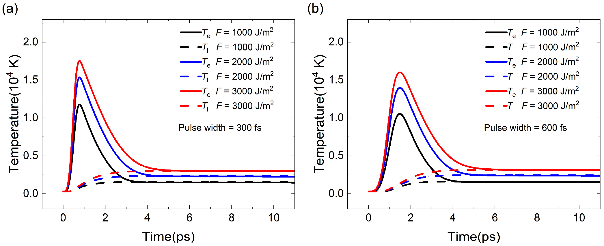
When the pulse duration tp was fixed, increasing the laser fluence F enhanced the energy input, allowing the electron system to absorb more energy within the same time period. This strengthened the transient excitation of electrons and increased both the peak electron temperature and the duration of the high-temperature state [24,38]. Correspondingly, the higher electron temperature and longer high-temperature duration enabled more energy to be transferred to the lattice through electron–lattice coupling heat transfer, thereby increasing the electron–lattice equilibrium temperature. As shown in Figure 1a, when the pulse duration is tp = 300 fs, increasing the laser fluence from 1000 J/m2 to 3000 J/m2 led to an overall rise in electron temperature. The peak electron temperature increased from 11,780 K to 17,520 K. Meanwhile, the width of electron temperature distribution also increased significantly, and the electron–lattice equilibrium temperature rose. A similar trend was observed for both the electron and lattice temperatures at tp = 600 fs, as shown in Figure 1b.

3.1.2. Effect of Pulse Duration on Electron and Lattice Temperatures

When the laser fluence remained unchanged, the pulse duration modified the temporal distribution of laser energy input. A shorter pulse duration corresponded to a higher peak power density, allowing the electron system to accumulate stronger instantaneous energy within a short time and reach a higher peak electron temperature [39]. Meanwhile, the higher temperature rise of the electron system promoted faster energy transfer to lattice through electron–lattice coupling, causing the lattice temperature to increase more rapidly.
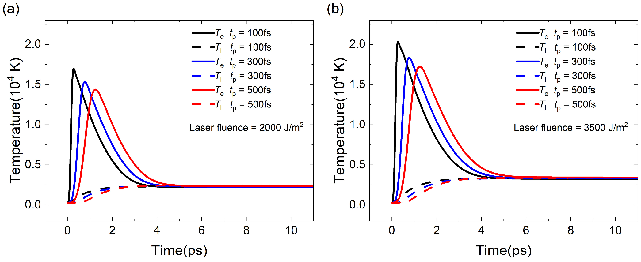
Figure 2a and Figure 2b showed the effect of pulse duration on surface temperature evolution under fixed laser fluences of F = 2000 J/m2 and F = 3500 J/m2, respectively. As the pulse duration increased from 100 fs to 500 fs, the peak electron temperature decreased significantly. This indicated that a longer pulse duration weakened the instantaneous heating ability of the electron system.
Wang et al. investigated the evolution of electron and lattice temperatures in pure Fe under femtosecond laser irradiation [40]. Using the parameters provided in the reference, the temperature evolution was calculated under a pulse duration of 200 fs and laser fluences of 75, 125, and 175 J/m2. The calculated peak electron temperatures were 1739.1 K, 2294.9 K, and 2765.1 K, respectively. Compared with the data extracted from the figures in the reference, the maximum absolute deviation was 55.5 K, and the maximum relative error was approximately 2.5%. This comparison verified the reliability of the electron-temperature calculation module used in the present study.

3.2. Net Charge Density Distribution

3.2.1. Effect of Laser Fluence on Net Charge Density

Before femtosecond laser irradiation, positive and negative charges inside the material remained balanced, and the initial electron number density was Ne0. After laser irradiation, electrons gain energy and electron emission may occur at the surface. As a result, the residual electron number density, Ne, in the near-surface region changed, breaking the original charge balance and generating a net charge distribution. Since this charge imbalance process exhibited obvious near-surface localization, electron diffusion compensated for the decrease in electron number density in the near-surface region, causing the charge imbalance state to evolve gradually with time.
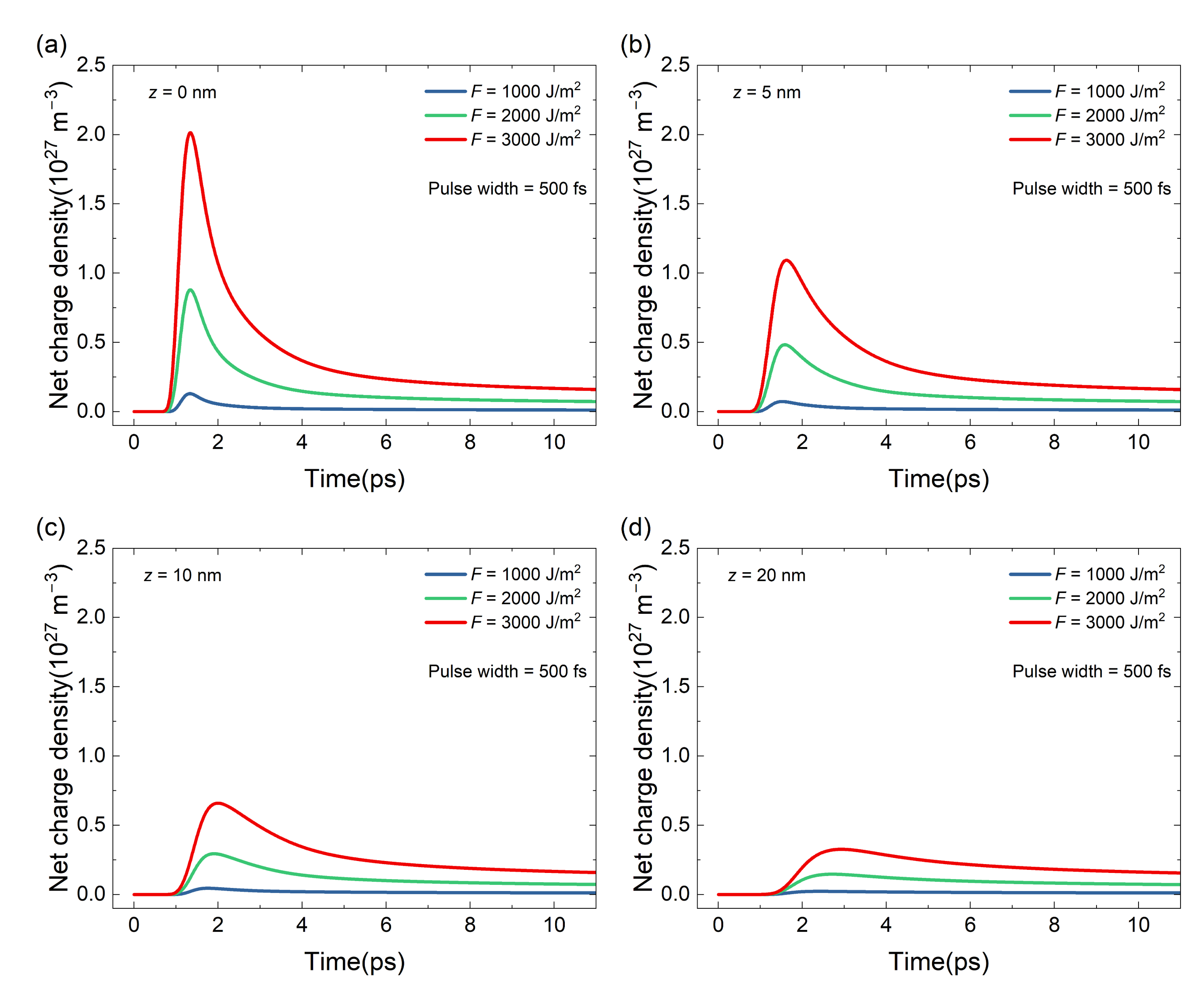
Increasing the laser fluence enhances the transient excitation of electron system and electron emission intensity [38]. Consequently, the degree of charge imbalance formed in the near-surface region was enhanced, and a longer time was required for charge balance to be re-established. As shown in Figure 3, under tp = 500 fs, as the laser fluence increased from 1000 J/m2 to 3000 J/m2, the peak net charge density ((Ne0Ne)max) at each depth position increased significantly. Meanwhile, the temporal width of curves at different depths also increased, indicating that the duration of the net charge imbalance state was markedly prolonged. By comparing different depth positions, it was observed that the surface position was most strongly affected by electron escape. At the position of z = 0 nm in Figure 3a, the net charge density was the highest, and the charge imbalance characteristic was the most pronounced. In Figure 3b–d, as the depth increases, the direct influence of electron emission weakened. The generation of net charge mainly depended on electron diffusion toward the surface, so the net charge density decreased significantly with increasing depth.

3.2.2. Effect of Pulse Duration on Net Charge Density

The net charge density was jointly affected by the electron emission intensity, emission duration, and electron diffusion compensation. At a fixed laser fluence, a shorter pulse duration caused the laser energy to be deposited within a shorter time, resulting in a higher electron emission rate but a shorter emission duration. Therefore, the compensation effect of electron diffusion on the near-surface charge imbalance was relatively limited. As the pulse duration increased, the laser power density decreased and the electron emission rate decreased, while the electron emission duration became longer. During the continuous electron emission process, an electron concentration gradient existed between the near-surface electron-depleted region and the interior of the material, which drove internal electrons to continuously diffuse toward the near-surface region and compensate for the local charge imbalance. The influence range of the electron diffusion compensation effect could be approximately characterized by the characteristic diffusion distance LD ≈ √(2 De tD) [41], where tD denoted the electron diffusion time. When the pulse duration increased, the electron emission duration was prolonged, and the electron diffusion time tD was also extended. Therefore, the influence range of electron diffusion compensation, LD, increased accordingly. This indicated that, during the electron emission process, a longer pulse duration allowed electron diffusion to compensate for the near-surface charge imbalance over a longer time, thereby making the diffusion compensation effect more pronounced.
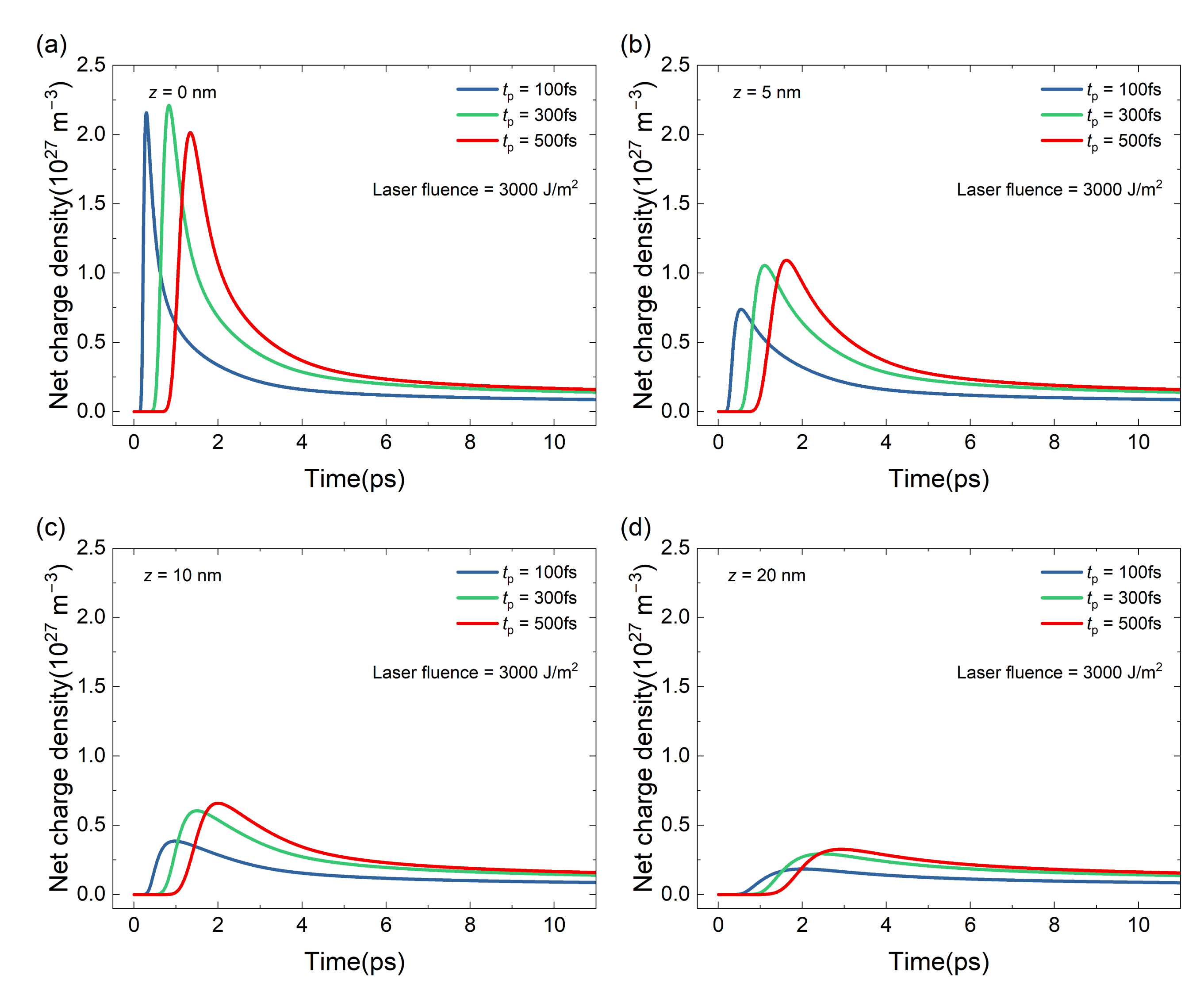
As shown in Figure 4a, at the surface position of z = 0 nm, under the condition of F = 3000 J/m2, when the pulse duration increased from 100 fs to 300 fs, the laser interaction time was still relatively short, and the compensation effect of internal electron diffusion on the surface charge imbalance was not yet obvious. Although the electron emission rate decreased, the cumulative effect caused by the longer emission duration dominated. Therefore, the peak net charge density increased with increasing pulse duration.
When the pulse duration further increased to 500 fs, although the electron emission duration was further extended, the electron emission intensity continued to decrease. Meanwhile, the longer interaction time enhanced the compensation of electron depletion by electron diffusion, resulting in a lower peak surface net charge density under the 500 fs condition than under the 300 fs condition.
Unlike the surface position, the net charge density at deeper positions was more strongly affected by the time-accumulation effect. As shown in Figure 4b–d, the peak net charge density at z = 5, 10, and 20 nm showed an increasing trend with increasing pulse duration. However, as the depth further increased, the enhancement effect of increasing pulse duration on the peak net charge density gradually weakened.

4. Discussion

4.1. Influence of Laser Parameters on Peak Electron Temperature

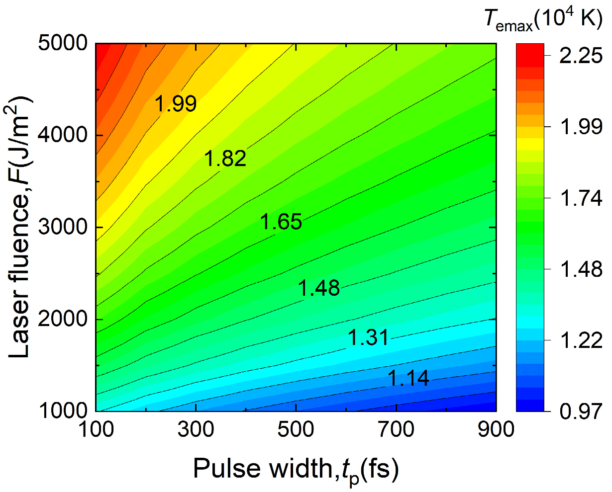
Laser fluence and pulse duration jointly affected the temperature evolution by changing total energy input, energy input power, and electron–lattice heat transfer time. To further compare the differences in transient electron excitation intensity under different parameter combinations, Figure 5 presents the contour distribution of peak electron temperature under different laser fluence and pulse durations. It was observed that the high-value region of Temax was mainly concentrated in the parameter combination of high laser fluence and short pulse duration. This indicated that, within this parameter range, laser energy was deposited in a concentrated manner over a short time, leading to a stronger instantaneous excitation of the electron system. In contrast, the low-value region was located in the range of low laser fluence and long pulse duration, where the energy input was lower and the energy deposition process was more dispersed, resulting in a weaker transient electron excitation.
The contour distribution was denser in the low-fluence region, while the spacing between contours increased in the high-fluence region. This indicated that, under relatively low laser fluence, Temax was more sensitive to the increase in F. As the laser fluence increased, the increase in Temax with F gradually decreased. This variation was related to the electron heat capacity and electron–lattice coupling. As the electron temperature increased, the electron heat capacity increased, meaning that more energy was required for further heating of the electron system. Meanwhile, a higher electron temperature increased the temperature difference between electrons and lattice, and enhanced electron–lattice coupling heat transfer, allowing more electron energy to be transferred to the lattice system. Therefore, although Temax still increased with increasing F in the high-fluence region, its rate gradually decreased [38].

4.2. Influence of Laser Parameters on Peak Net Charge Density

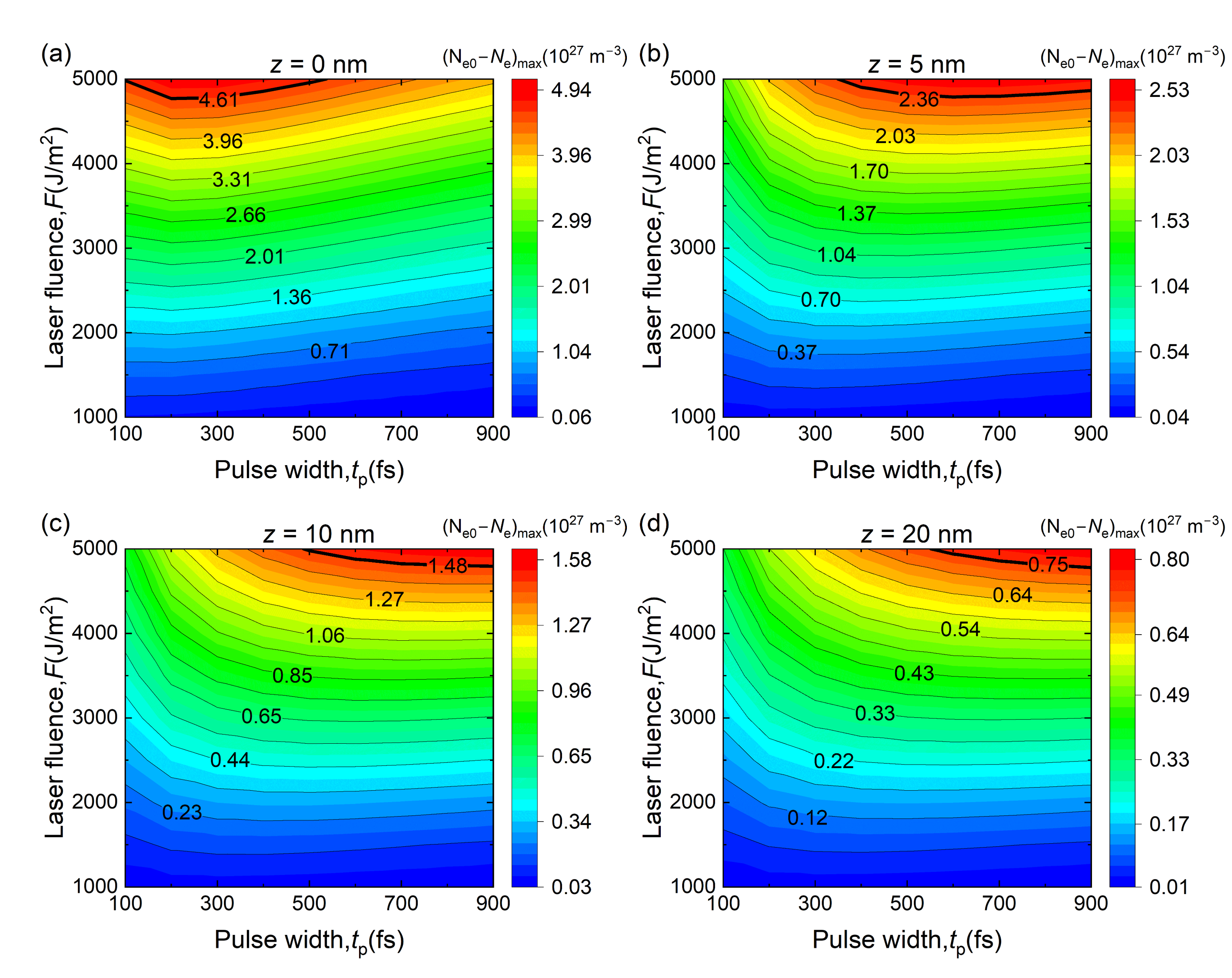
Figure 6 shows the distribution of peak net charge density (Ne0Ne)max at different depths as a function of laser fluence and pulse duration. At the surface position of z = 0 nm, a higher value of (Ne0Ne)max represents a greater degree of net charge accumulation. At deeper positions, a higher value of (Ne0Ne)max indicates that the charge imbalance was maintained to a greater depth, reflecting its extension along the depth direction.
As shown in Figure 6, the contour lines corresponding to approximately 94% of the maximum value in each subplot were highlighted in bold to more intuitively compare the positional changes of the high-value regions at different depths. This contour line did not represent a specific physical threshold. Figure 6 showed that the high-value regions of net charge density at different depths all correspond to high laser fluence conditions above 4500 J/m2, whereas the corresponding pulse-duration ranges varied with depth. As shown in Figure 6a, the high-value region at z = 0 nm was mainly concentrated in the relatively short pulse-duration range of tp = 100–500 fs. With increasing depth, the pulse-duration range corresponding to the high-value region gradually shifted toward longer pulse durations. In Figure 6b, at z = 5 nm, the high-value region was mainly located in the range of tp = 400–900 fs. Compared with Figure 6b, when the observation depth increased to 10 nm in Figure 6c, the pulse-duration range corresponding to high net charge density still continued to shift toward longer pulse durations, but this tendency became weaker. For z = 20 nm, the further shift of the high-value region was no longer obvious. In other words, increasing the pulse duration promoted the extension of the net charge-density distribution toward deeper regions, but this extension tendency gradually weakened with increasing depth.
This distribution trend indicated that the favorable pulse-duration range for net charge accumulation at the surface was different from that for its extension along the depth direction. As a result, the favorable pulse-duration ranges corresponding to different depths exhibited a certain overlap. This overlapping region represented a balance between the intensity of surface net charge accumulation and the ability of the charge imbalance to extend in the depth direction. Under these parameter combinations, relatively high net charge accumulation could be formed at the surface, while the charge-imbalance distribution could also extend to deeper positions.
During femtosecond laser irradiation, electron emission can disturb the local charge balance near the material surface, resulting in an obvious net charge density distribution. Previous studies have shown that the near-surface charge imbalance distribution is an important basis for the formation of transient Coulomb electric field. When the local electric field strength reaches the threshold value, the non-thermal ablation of surface positive ions may be induced. For grain-oriented silicon steel, when laser fluence and pulse duration were varied simultaneously, the peak magnitude, distribution depth, and duration of net charge density all changed with the laser parameters. These characteristics therefore reflect the strength of local near-surface charge imbalance. In general, a higher surface net charge density and a deeper charge-imbalance distribution are more favorable for the formation of transient Coulomb fields.

5. Conclusions

Based on the two-temperature model and electron transport model, this study analyzed the near-surface electron temperature response and the evolution of net charge density (Ne0Ne) in grain-oriented silicon steel under femtosecond laser irradiation.
(1)
During the initial stage of laser irradiation, the electron system heated up rapidly and formed an obvious non-equilibrium state with the lattice system. The peak electron temperature was jointly regulated by laser fluence and pulse duration.
(2)
Increasing laser fluence increased the net charge density at all depth positions. With increasing pulse duration, the net charge density at the surface first increased and then decreased, whereas the net charge density in the internal region increased monotonically.
(3)
The accumulation of net charge at the surface was mainly determined by the peak electron temperature and instantaneous emission intensity, whereas net charge accumulation at deeper positions depended more strongly on the sustained effects of electron emission and transport processes.

Supplementary Materials

The following supporting information can be downloaded at: https://www.mdpi.com/article/10.3390/met16070799/s1, Table S1: Source data corresponding to Figure 1; Table S2: Source data corresponding to Figure 2; Table S3: Source data corresponding to Figure 3; Table S4: Source data corresponding to Figure 4; Table S5: Source data corresponding to Figure 5; Table S6: Source data corresponding to Figure 6.

Author Contributions

Conceptualization, G.L. and Y.S.; methodology, H.Z., Y.Y., and Y.S.; software, H.Z.; validation, H.Z. and Y.S.; formal analysis, G.L., H.Z., and Y.S.; investigation, H.Z. and Y.Y.; resources, G.L., Y.Y., and F.Z.; data curation, H.Z. and Y.Y.; writing—original draft preparation, H.Z.; writing—review & editing, G.L., Y.Y., F.Z., and Y.S.; visualization, H.Z. and F.Z.; supervision, Y.S.; project administration, G.L. and Y.S.; and funding acquisition, Y.S. All authors have read and agreed to the published version of the manuscript.

Funding

This research was funded by the National Natural Science Foundation of China, grant number 52371022.

Data Availability Statement

The original contributions presented in the study are included in the article/Supplementary Material, further inquiries can be directed to the corresponding author.

Conflicts of Interest

Guobao Li and Yongjie Yang are employees of Baoshan Iron & Steel Co., Ltd. The authors declare no conflicts of interest. The funder had no role in the design of the study; in the collection, analyses, or interpretation of data; in the writing of the manuscript; or in the decision to publish the results.

Appendix A

Table A1. Definition of symbols used in the mathematical model.
SymbolDefinitionUnit
FLaser fluenceJ/m2
tpPulse durationfs
RReflectivity-
αOptical absorption coefficientm−1
SLaser source termW/m3
TeElectron temperatureK
TlLattice temperatureK
CeElectron heat capacityJ/m3/K
ClLattice heat capacityJ/m3/K
Keelectron thermal conductivityW/m/K
Kllattice thermal conductivityW/m/K
GrElectron–lattice coupling factorW/m3/K
NeElectron densitym−1
Ne0Initial electron densitym−1
Ne0NeNet charge density expressed as electron density differencem−1
DeElectron diffusion coefficientm/s2
LpCharacteristic electron diffusion lengthm
EfFermi energyeV
TFFermi temperatureK
μChemical potentialeV
eφwWork function energyeV
A0Richardson–Dushman constantA/m2/K2
kBBoltzmann constantJ/K
eElementary chargeC

References

  1. Jahangiri, M.R.; Bayani, H.; Ardestani, M.; Mehdizadeh, M. Core Loss Reduction in Grain Oriented Silicon Steel Sheets by Two-Sided Laser Scribing in the Presence of a Magnetic Field. J. Alloys Compd. 2022, 891, 162080. [Google Scholar] [CrossRef] [Scilit]
  2. Iwata, K.; Ishiyama, K.; Suzuki, M.; Hashimoto, M.; Ueda, M.; Matuoka, Y.; Yasue, T.; Koshikawa, T.; Kotsugi, M.; Ohkochi, T. Quantitative Analysis of 90° Closure Domains Occurring by Compressive Stress in Fe3% Si (110) Steels. IEEE Trans. Magn. 2014, 50, 1–4. [Google Scholar] [CrossRef] [Scilit]
  3. Zhang, W.; Chen, J.; Lin, M.; Zhang, L.; Hu, Y.; Tang, S.; Lu, H.; Feng, J.; Li, R. The Influence of Laser Process Parameters on the Iron Loss of Grain-Oriented Silicon Steel. J. Mater. Res. Technol. 2024, 33, 2958–2969. [Google Scholar] [CrossRef] [Scilit]
  4. Abbruzzese, G.C. Effects of Secondary Grain Size on Laser Scribing Optimization in GO Electrical Steel: An Integrated Magnetic Core Losses Model and Experiments. J. Magn. Magn. Mater. 2026, 655, 174336. [Google Scholar] [CrossRef] [Scilit]
  5. Nesser, M.; Maloberti, O.; Salloum, E.; Dupuy, J.; Panier, S.; Pineau, C.; Birat, J.-P.; Fortin, J.; Dassonvalle, P. Impact of Ultra-Short Pulsed Laser (USPL) Ablation Process on Separated Loss Coefficients of Grain Oriented Electrical Steels. IEEE Trans. Magn. 2022, 58, 1–5. [Google Scholar] [CrossRef] [Scilit]
  6. Maloberti, O.; Nesser, M.; Salloum, E.; Dupuy, J.; Dassonvalle, P.; Pineau, C.; Panier, S.; Birat, J.P. Relative Control of Domains’ Structure in Grain-Oriented Electrical Steels by Ultra-Short Pulsed Laser Ablation Process. J. Magn. Magn. Mater. 2023, 580, 170279. [Google Scholar] [CrossRef] [Scilit]
  7. Leitz, K.-H.; Redlingshöfer, B.; Reg, Y.; Otto, A.; Schmidt, M. Metal Ablation with Short and Ultrashort Laser Pulses. Phys. Procedia 2011, 12, 230–238. [Google Scholar] [CrossRef] [Scilit]
  8. Wang, H.-J.; Yang, T. A Review on Laser Drilling and Cutting of Silicon. J. Eur. Ceram. Soc. 2021, 41, 4997–5015. [Google Scholar] [CrossRef] [Scilit]
  9. Putzer, M.; Ackerl, N.; Wegener, K. Geometry Assessment of Ultra-Short Pulsed Laser Drilled Micro-Holes. Int. J. Adv. Manuf. Technol. 2021, 117, 2445–2452. [Google Scholar] [CrossRef] [Scilit] [PubMed]
  10. Lee, D. Picosecond IR Pulsed Laser Drilling of Copper-Coated Glass/Epoxy Composite. IEEE Trans. Compon. Packag. Manuf. Technol. 2017, 7, 2066–2072. [Google Scholar] [CrossRef] [Scilit]
  11. Yu, J.; Han, W.; Suleiman, A.A.; Han, S.; Miao, N.; Ling, F.C.-C. Recent Advances on Pulsed Laser Deposition of Large-Scale Thin Films. Small Methods 2024, 8, 2301282. [Google Scholar] [CrossRef] [Scilit] [PubMed]
  12. Mueller, B.Y.; Rethfeld, B. Nonequilibrium Electron–Phonon Coupling after Ultrashort Laser Excitation of Gold. Appl. Surf. Sci. 2014, 302, 24–28. [Google Scholar] [CrossRef] [Scilit]
  13. Phillips, K.C.; Gandhi, H.H.; Mazur, E.; Sundaram, S.K. Ultrafast Laser Processing of Materials: A Review. Adv. Opt. Photonics 2015, 7, 684–712. [Google Scholar] [CrossRef] [Scilit]
  14. Anisimov, S.I.; Kapeliovich, B.L.; Perelman, T.L. Electron Emission from Metal Surfaces Exposed to Ultrashort Laser Pulses. Zh. Eksp. Teor. Fiz. 1974, 66, 375–377. [Google Scholar]
  15. Parris, G.; Goel, S.; Nguyen, D.T.; Buckeridge, J.; Zhou, X. A Critical Review of the Developments in Molecular Dynamics Simulations to Study Femtosecond Laser Ablation. Mater. Today Proc. 2022, 64, 1339–1348. [Google Scholar] [CrossRef] [Scilit]
  16. Vanwersch, P.; Schildermans, S.; Nagarajan, B.; Van Bael, A.; Castagne, S. Three-Dimensional Modelling of Femtosecond Laser Ablation of Metals. Lasers Manuf. Mater. Process. 2022, 9, 515–531. [Google Scholar] [CrossRef] [Scilit]
  17. Chen, C.; Spellauge, M.; Redka, D.; Auer, R.; Doñate, C.; Barcikowski, S.; Gökce, B.; Huber, H.P.; Zhigilei, L.V. Time-Resolved Probing and Modeling of Optical Signatures of Ultrashort Pulse Laser Spallation and Phase Explosion in Iron-Nickel Targets. Phys. Rev. B 2025, 111, 174301. [Google Scholar] [CrossRef] [Scilit]
  18. Lin, X.; Chen, H.; Jiang, S.; Zhang, C. A Coulomb Explosion Theoretical Model of Femtosecond Laser Ablation Materials. Sci. China Technol. Sci. 2012, 55, 694–701. [Google Scholar] [CrossRef] [Scilit]
  19. Bulgakova, N.M.; Stoian, R.; Rosenfeld, A.; Hertel, I.V.; Campbell, E.E.B. Electronic Transport and Consequences for Material Removal in Ultrafast Pulsed Laser Ablation of Materials. Phys. Rev. B 2004, 69, 054102. [Google Scholar] [CrossRef] [Scilit]
  20. Stoian, R.; Ashkenasi, D.; Rosenfeld, A.; Campbell, E.E.B. Coulomb Explosion in Ultrashort Pulsed Laser Ablation of Al2O3. Phys. Rev. B 2000, 62, 13167–13173. [Google Scholar] [CrossRef] [Scilit]
  21. Henyk, M.; Costache, F.; Reif, J. Femtosecond Laser Ablation from Sodium Chloride and Barium Fluoride. Appl. Surf. Sci. 2002, 186, 381–384. [Google Scholar] [CrossRef] [Scilit]
  22. Li, S.; Li, S.; Zhang, F.; Tian, D.; Li, H.; Liu, D.; Jiang, Y.; Chen, A.; Jin, M. Possible Evidence of Coulomb Explosion in the Femtosecond Laser Ablation of Metal at Low Laser Fluence. Appl. Surf. Sci. 2015, 355, 681–685. [Google Scholar] [CrossRef] [Scilit]
  23. Jiang, L.; Tsai, H.L. Plasma Modeling for Ultrashort Pulse Laser Ablation of Dielectrics. J. Appl. Phys. 2006, 100, 023116. [Google Scholar] [CrossRef] [Scilit]
  24. Omeñaca, L.; Gomez-Aranzadi, M.; Ayerdi, I.; Castaño, E. Numerical Simulation and Experimental Validation of Ultrafast Laser Ablation on Aluminum. Opt. Laser Technol. 2024, 170, 110283. [Google Scholar] [CrossRef] [Scilit]
  25. Chen, J.K.; Tzou, D.Y.; Beraun, J.E. A Semiclassical Two-Temperature Model for Ultrafast Laser Heating. Int. J. Heat Mass Transf. 2006, 49, 307–316. [Google Scholar] [CrossRef] [Scilit]
  26. Chen, J.K.; Latham, W.P.; Beraun, J.E. The Role of Electron–Phonon Coupling in Ultrafast Laser Heating. J. Laser Appl. 2005, 17, 63–68. [Google Scholar] [CrossRef] [Scilit]
  27. Nedialkov, N.N.; Imamova, S.E.; Atanasov, P.A. Ablation of Metals by Ultrashort Laser Pulses. J. Phys. D Appl. Phys. 2004, 37, 638–643. [Google Scholar] [CrossRef] [Scilit]
  28. Cheng, C.-W.; Wang, S.Y.; Chang, K.P.; Chen, J.K. Femtosecond Laser Ablation of Copper at High Laser Fluence: Modeling and Experimental Comparison. Appl. Surf. Sci. 2016, 361, 41–48. [Google Scholar] [CrossRef] [Scilit]
  29. Hirayama, Y.; Atanasov, P.A.; Obara, M.; Nedialkov, N.N.; Imamova, S.E. Femtosecond Laser Ablation of Crystalline Iron: Experimental Investigation and Molecular Dynamics Simulation. Jpn. J. Appl. Phys. 2006, 45, 792. [Google Scholar] [CrossRef] [Scilit]
  30. Wang, S.Y.; Ren, Y.; Cheng, C.-W.; Chen, J.K.; Tzou, D.Y. Micromachining of Copper by Femtosecond Laser Pulses. Appl. Surf. Sci. 2013, 265, 302–308. [Google Scholar] [CrossRef] [Scilit]
  31. Riffe, D.M.; More, R.M.; Wang, X.Y.; Downer, M.C.; Fisher, D.L.; Tajima, T.; Erskine, J.L. Femtosecond Thermionic Emission from Metals in the Space-Charge-Limited Regime. J. Opt. Soc. Am. B 1993, 10, 1424. [Google Scholar] [CrossRef] [Scilit]
  32. Balasubramni, T.; Kim, S.H.; Jeong, S.H. Enhanced Two Temperature Modeling of Ultrashort Laser Ablation for the Investigation of Thermionic Emission Characteristics. Appl. Surf. Sci. 2009, 255, 9601–9604. [Google Scholar] [CrossRef] [Scilit]
  33. Maloberti, O.; Nesser, M.; Dupont, P.; Dupuy, J.; Henrottin, A.; Birat, J.-P.; Pineau, C.; Panier, S. Semi-Quantic Thermo-Optical Modelling of the Ultra-Short Pulsed Laser Ablation Process on Grain-Oriented Electrical Steels. Opt. Laser Technol. 2025, 189, 113004. [Google Scholar] [CrossRef] [Scilit]
  34. Jiang, L.; Tsai, H.-L. Improved Two-Temperature Model and Its Application in Ultrashort Laser Heating of Metal Films. J. Heat Transf. 2005, 127, 1167–1173. [Google Scholar] [CrossRef] [Scilit]
  35. Ueda, K.; Shimizu, R. Studies of Initial Oxidation on Silicon-Iron Alloy (100) by Means of Work Function and Auger Electron Spectroscopy. Appl. Phys. Lett. 1973, 22, 393–395. [Google Scholar] [CrossRef] [Scilit]
  36. Balasubramani, T.; Jeong, S.H. Simulation of the Thermionic Emission during Ultrashort Pulse Laser Ablation of Metals. In Proceedings of the Journal of Physics: Conference Series, Banff, AB, Canada, 11–16 September 2005; IOP Publishing: Bristol, UK, 2007; Volume 59, pp. 595–599. [Google Scholar]
  37. Lu, X.; Tian, Y.; Wang, Z.; Wang, X.; Liang, S.Y. Numerical Simulation and Parameters Optimization of Invar 36 Alloy Multi-Pulse Femtosecond Laser Processing. Int. J. Precis. Eng. Manuf. 2025, 26, 1075–1089. [Google Scholar] [CrossRef] [Scilit]
  38. Wang, T.; Guo, J.; Shao, J.; Wang, D.; Chen, A.; Jin, M. Ultrafast Thermionic Emission from Metal Irradiated Using a Femtosecond Laser and an Electric Field in Combination. Phys. Plasmas 2015, 22, 033106. [Google Scholar] [CrossRef] [Scilit]
  39. Metzner, D.; Olbrich, M.; Lickschat, P.; Horn, A.; Weißmantel, S. Experimental and Theoretical Determination of the Effective Penetration Depth of Ultrafast Laser Radiation in Stainless Steel. Lasers Manuf. Mater. Process. 2020, 7, 478–495. [Google Scholar] [CrossRef] [Scilit]
  40. Wang, Z.; Fu, W.; Zhang, R. Numerical simulation of femtosecond laser multi pulse ablation of metal iron. Infrared Laser Eng. 2019, 48, 70602. [Google Scholar] [CrossRef] [Scilit]
  41. Crank, J. The Mathematics of Diffusion; Clarendon Press: Oxford, UK, 1975; 414p. [Google Scholar]
Figure 1. Surface electron temperature and lattice temperature under different laser fluences at pulse durations of: (a) tp = 300 fs; (b) tp = 600 fs.
Metals 16 00799 g001
Figure 2. Surface electron temperature and lattice temperature under different pulse durations at laser fluences of: (a) F = 2000 J/m2; (b) F = 3500 J/m2.
Metals 16 00799 g002
Figure 3. Time-dependent evolution of net charge density at different depths under laser fluences of F = 1000 J/m2–3000 J/m2 with a pulse duration of tp = 500 fs: (a) z = 0 nm; (b) z = 5 nm; (c) z = 10 nm; (d) z = 20 nm.
Metals 16 00799 g003
Figure 4. Time-dependent evolution of net charge density at different depths under different pulse durations of tp = 100 fs–500 fs at a laser fluence of F = 3000 J/m2: (a) z = 0 nm; (b) z = 5 nm; (c) z = 10 nm; (d) z = 20 nm.
Metals 16 00799 g004
Figure 5. Distribution of peak electron temperature Temax under different laser parameters.
Metals 16 00799 g005
Figure 6. Distribution of peak net charge density at different depths dependent on laser fluence and pulse duration: (a) z = 0 nm; (b) z = 5 nm; (c) z = 10 nm; (d) z = 20 nm.
Metals 16 00799 g006
Disclaimer/Publisher’s Note: The statements, opinions and data contained in all publications are solely those of the individual author(s) and contributor(s) and not of MDPI and/or the editor(s). MDPI and/or the editor(s) disclaim responsibility for any injury to people or property resulting from any ideas, methods, instructions or products referred to in the content.