
Optimization of Forming Parameters and Forming Strategy for Stamping of Novel Ultra-Thin Super Ferritic Stainless Steel Bipolar Plates Based on Numerical Simulation


Abstract
1. Introduction
2. Establishment of the FEM for Stamping Forming
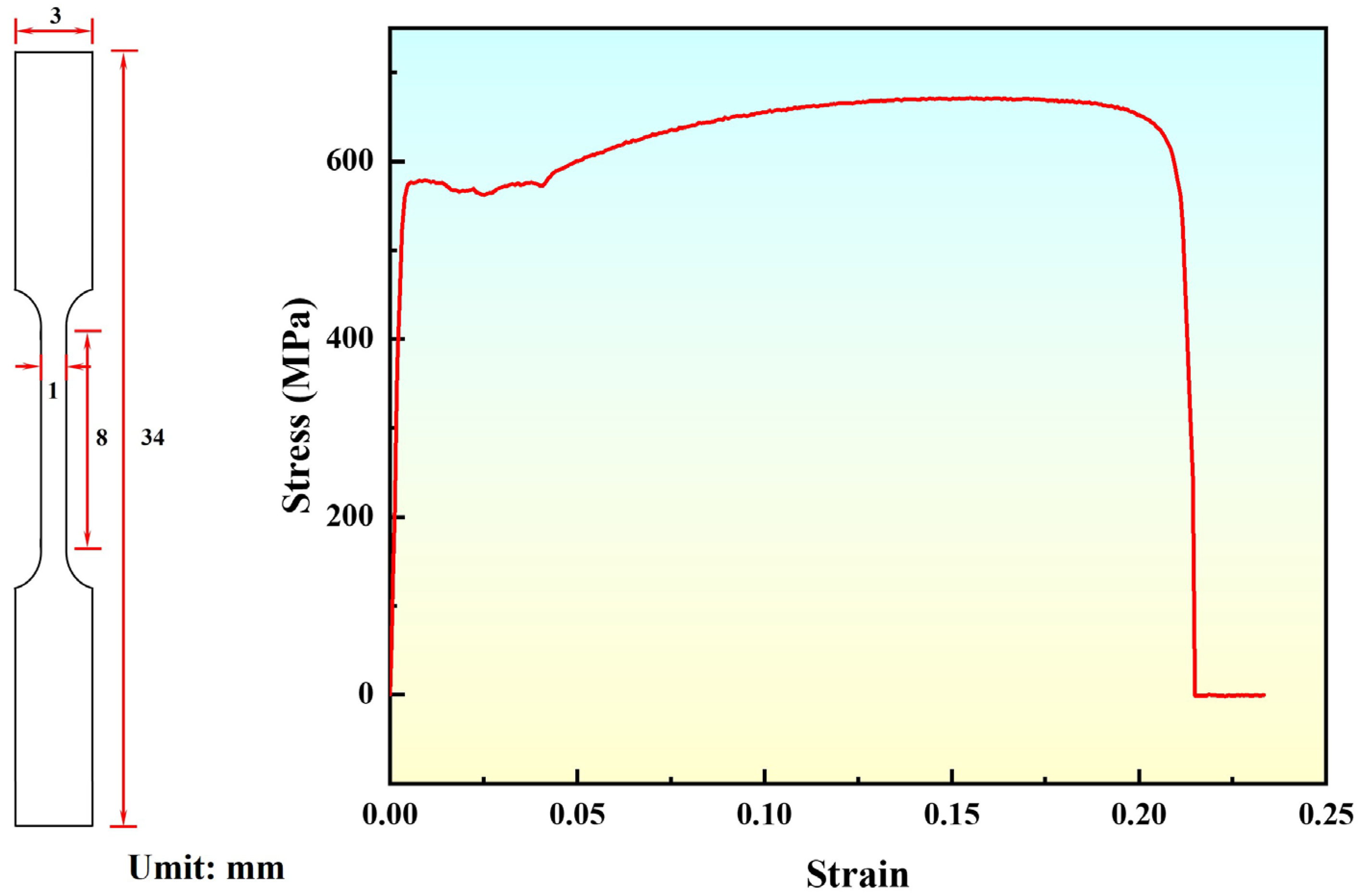
2.1. Materials
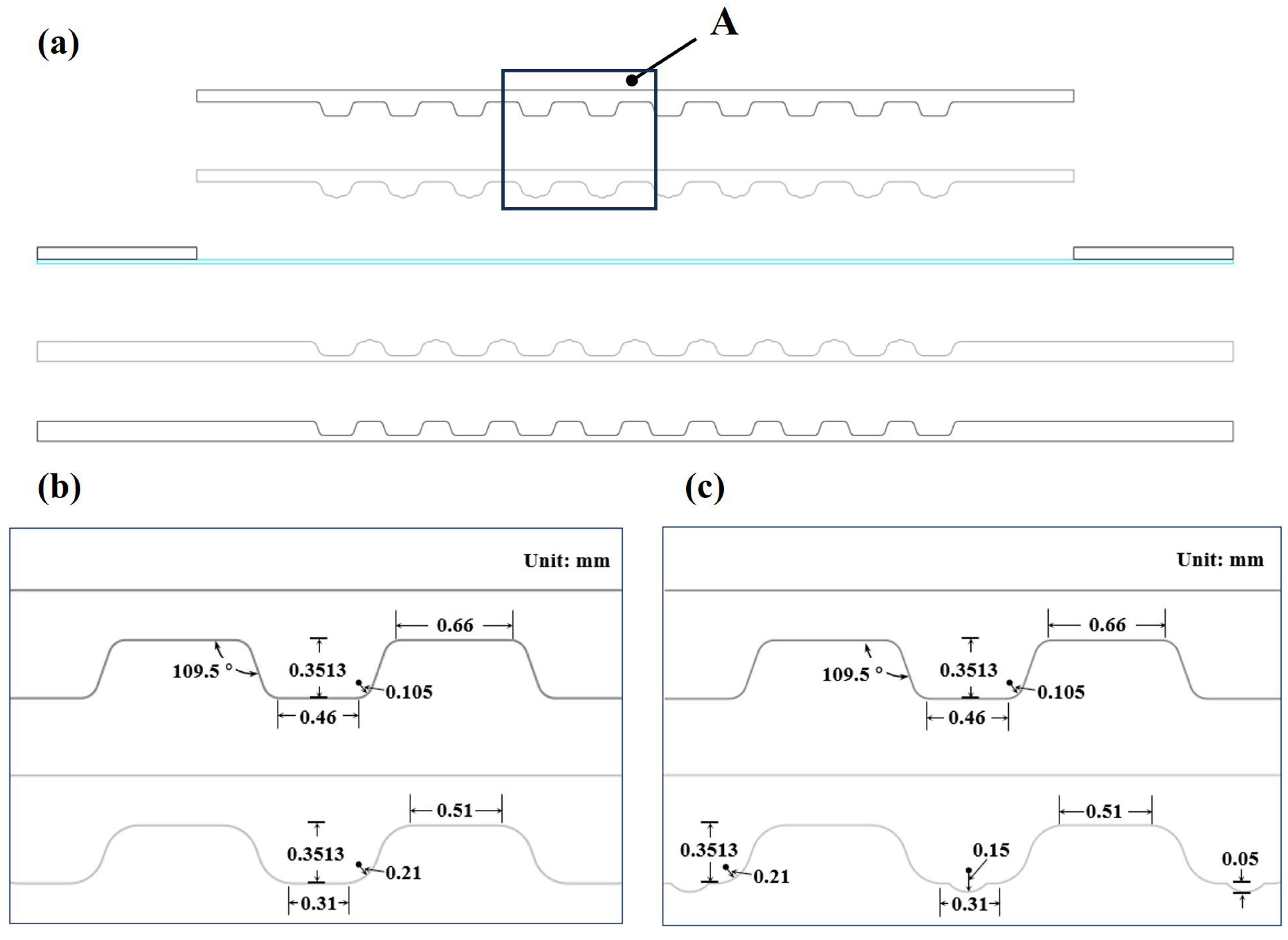
2.2. Die Design
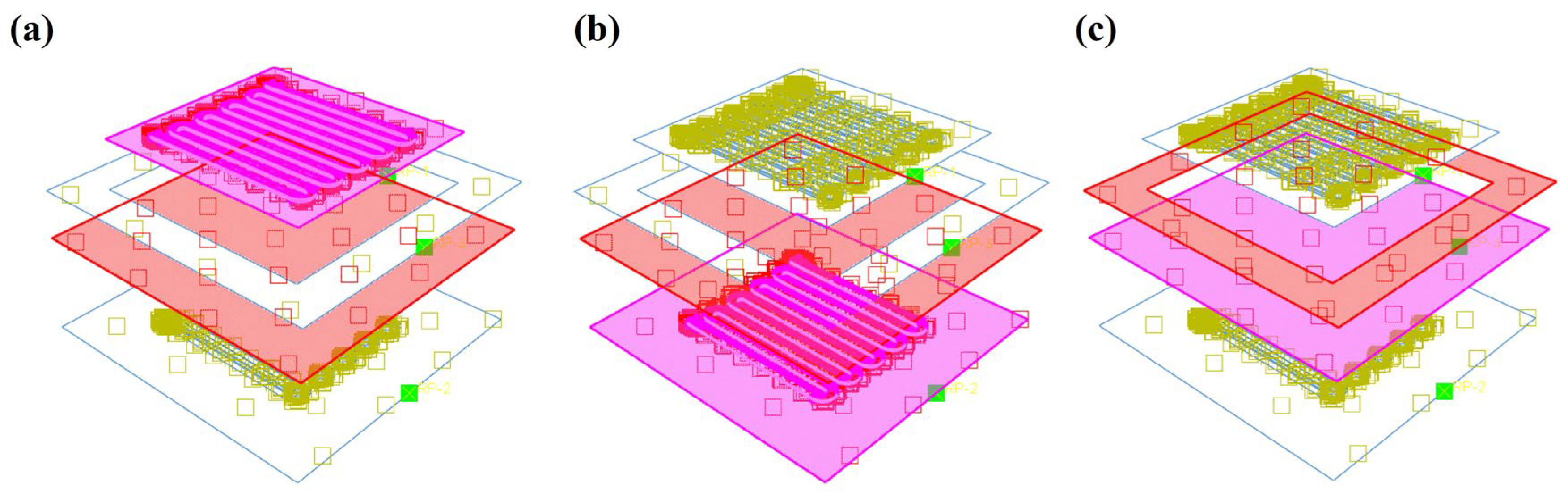
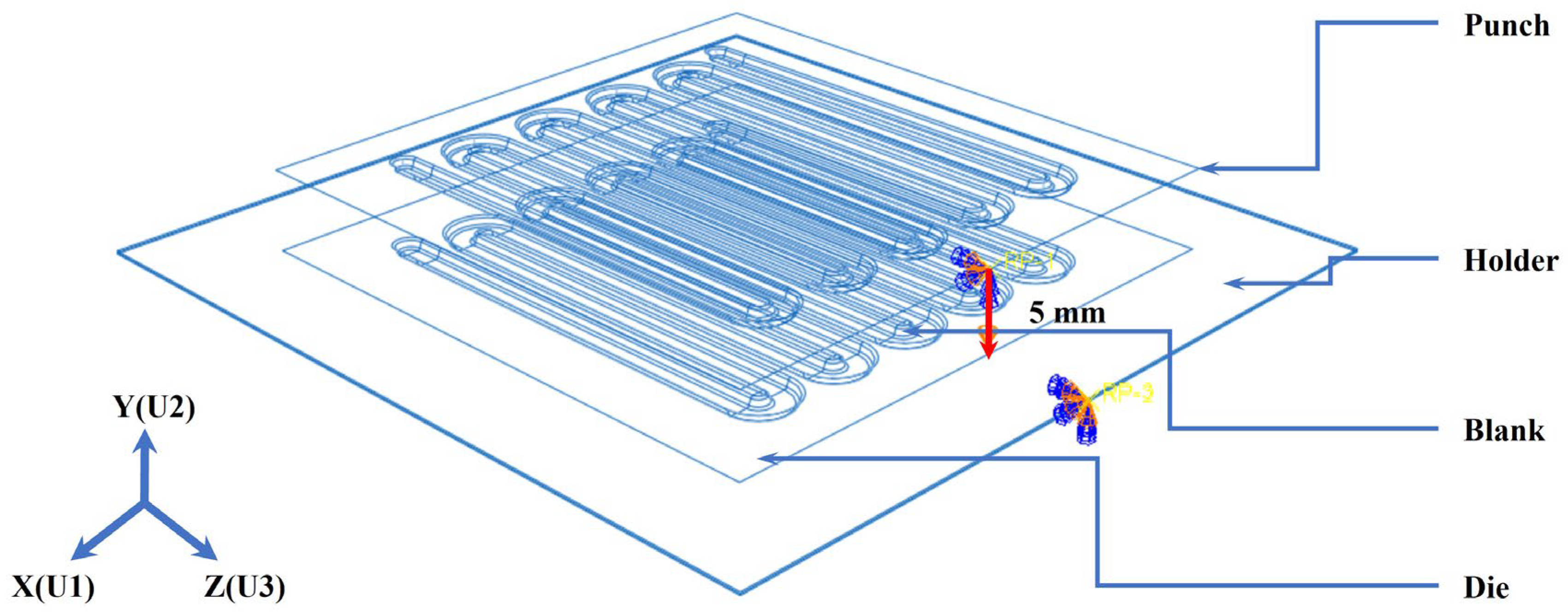
2.3. Establishing the Finite Element Model
2.4. FEM for Stamping Forming of Bipolar Plate
3. Results and Discussion
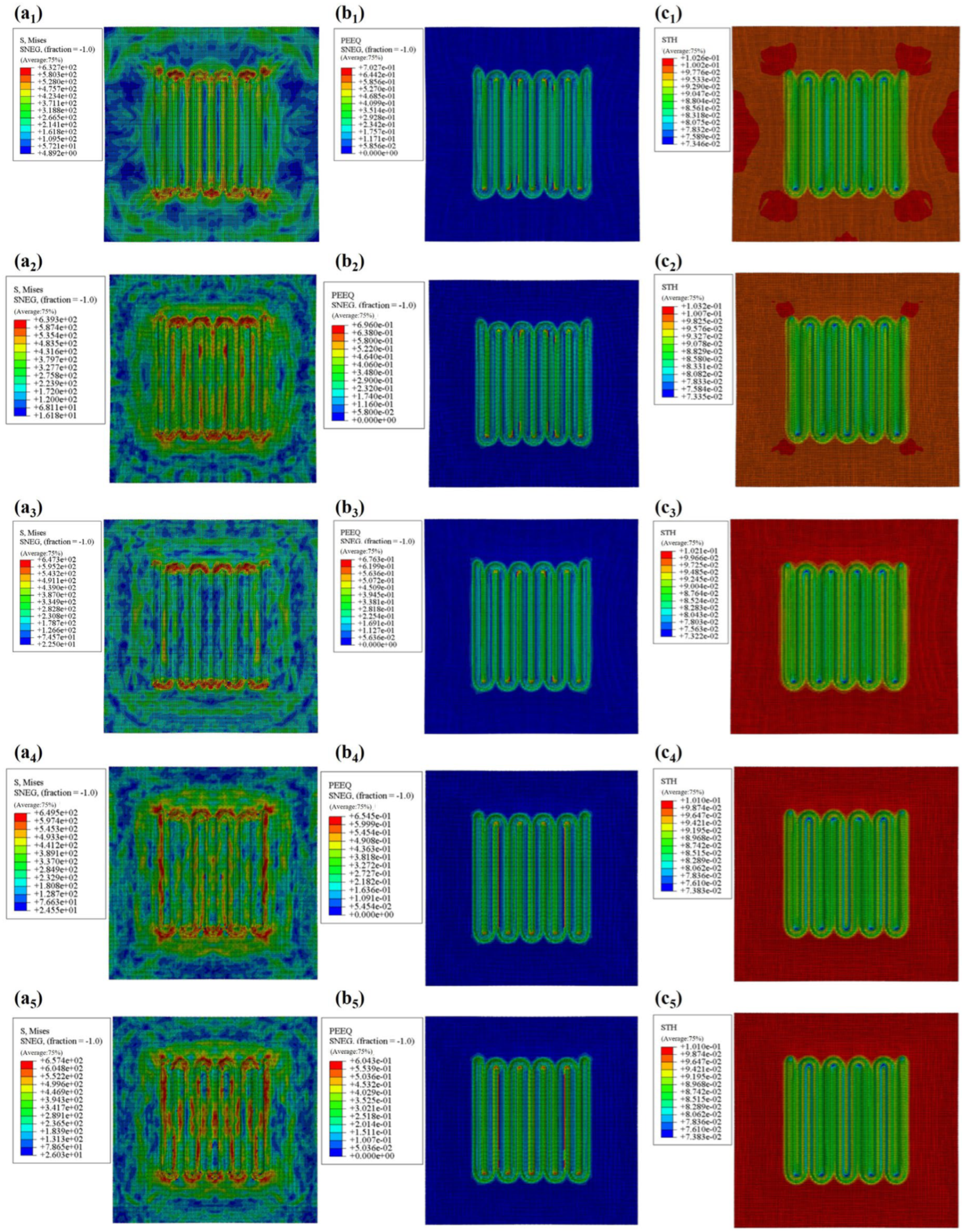
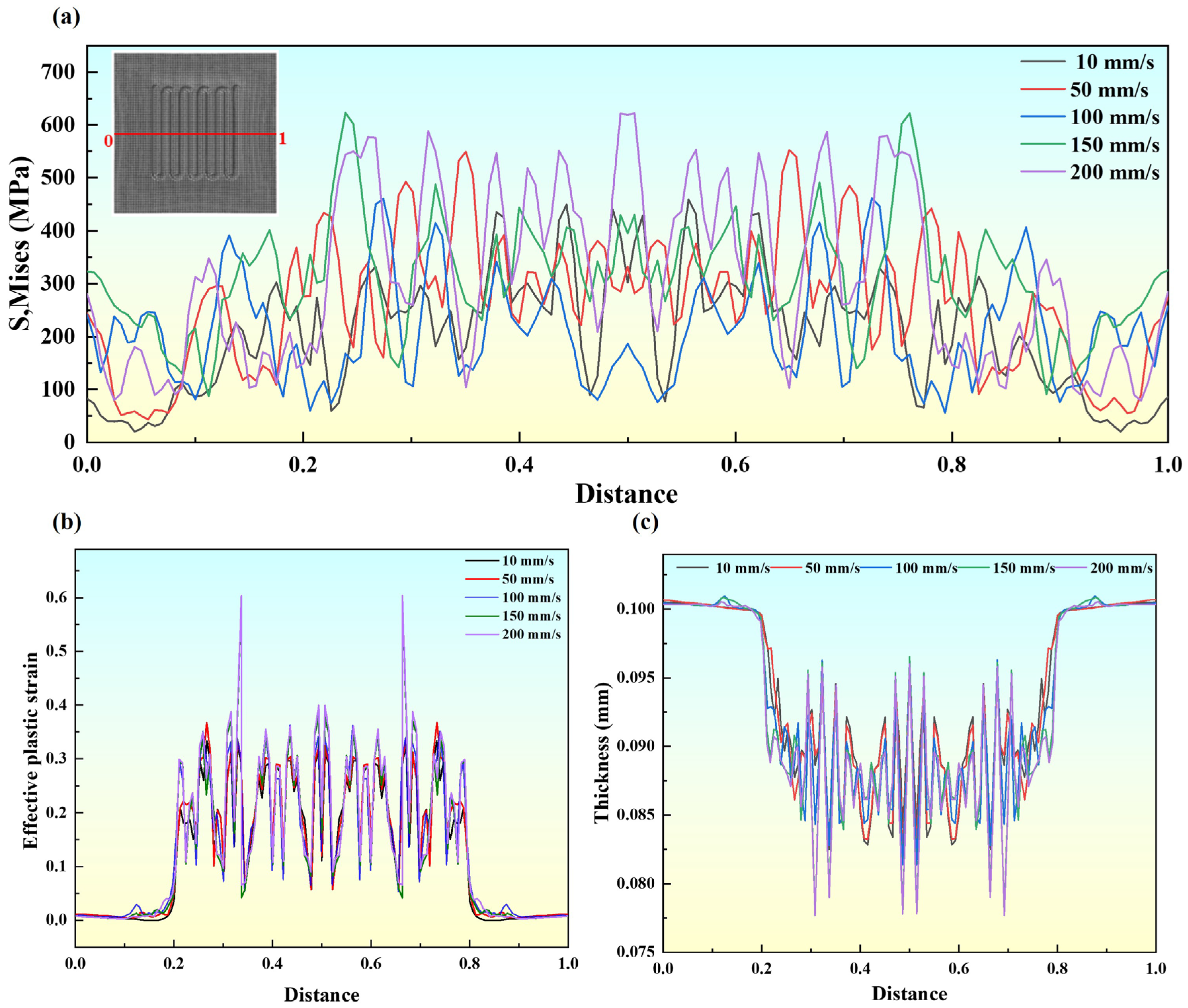
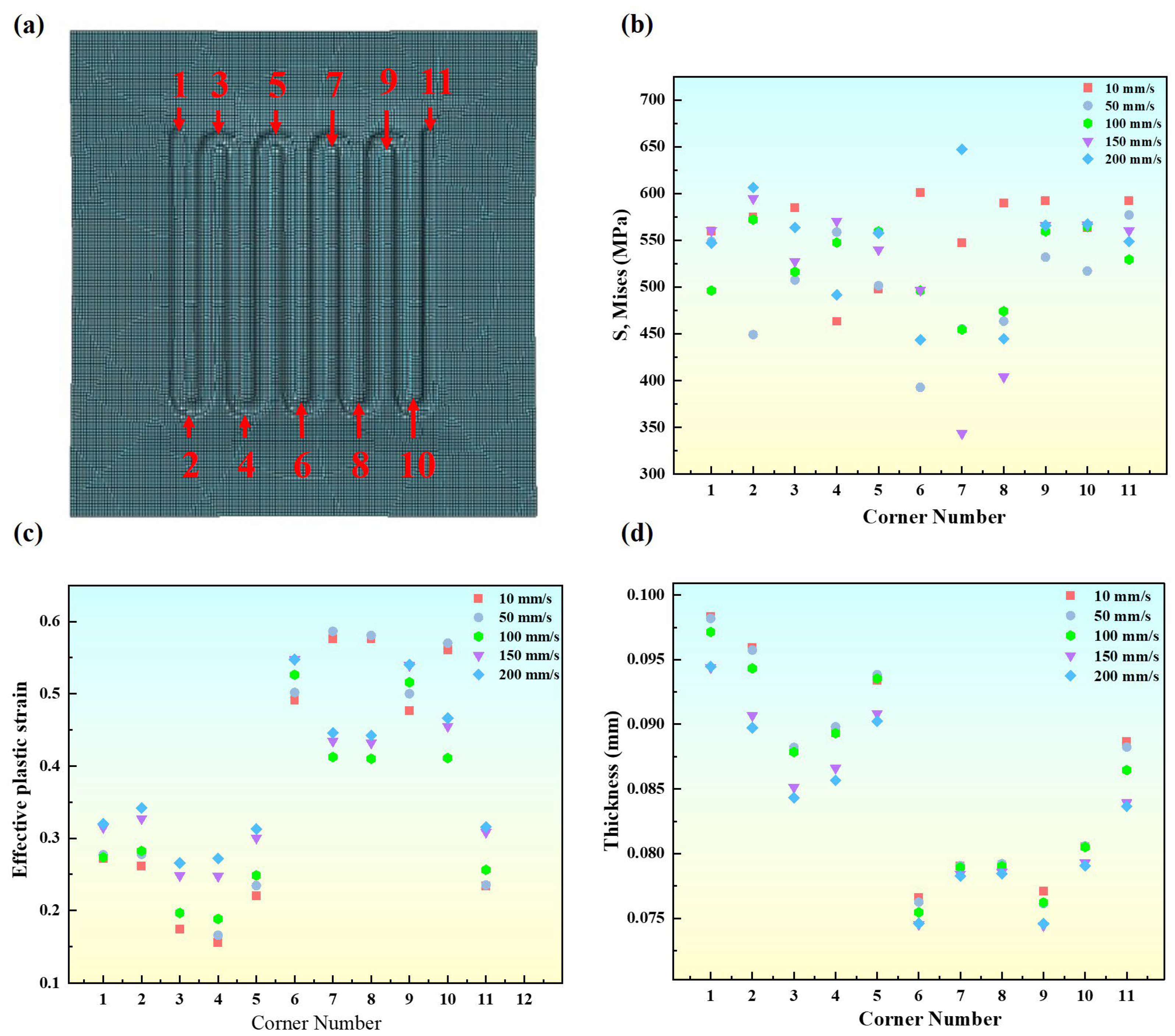
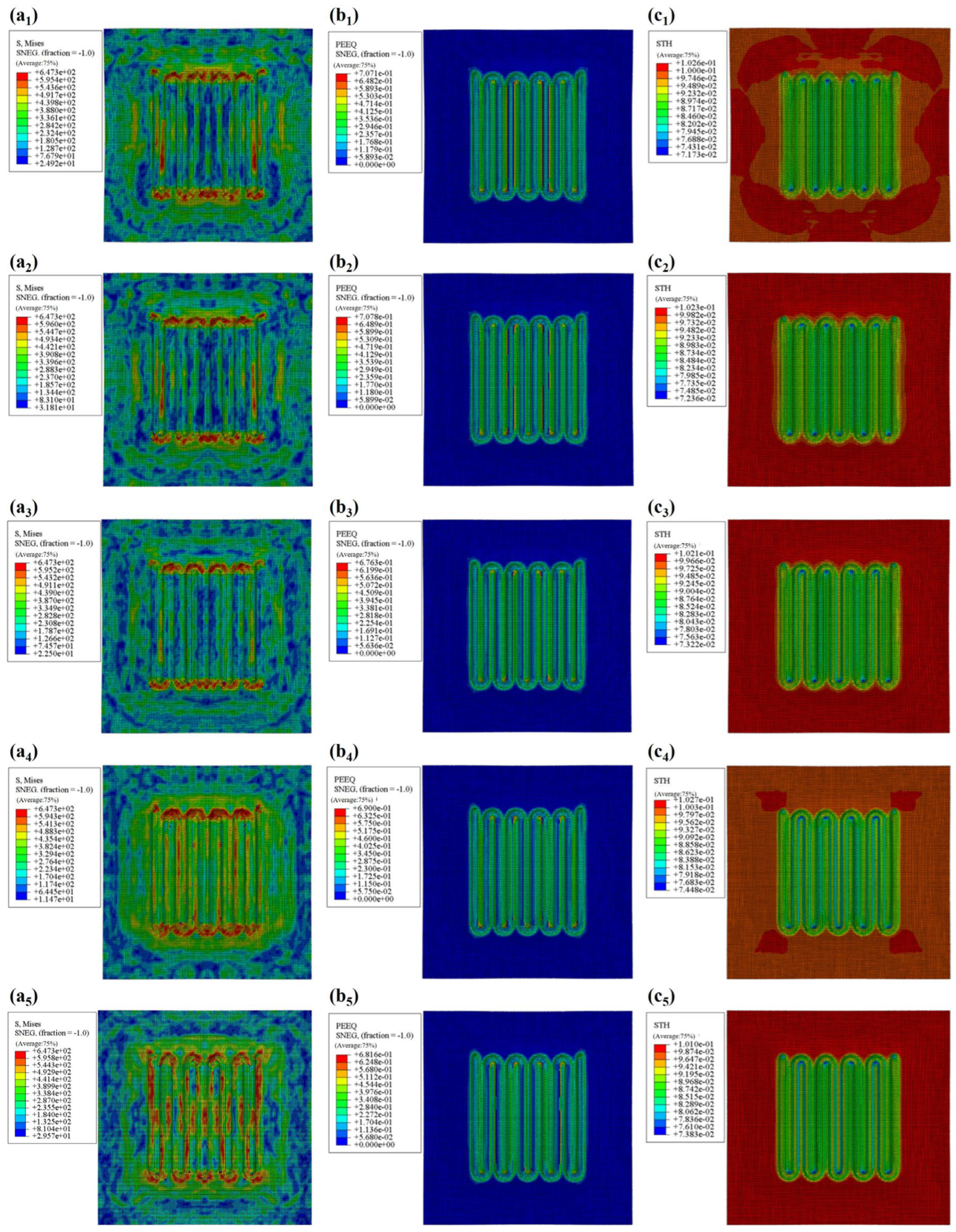
3.1. The Influence of Process Parameters on the Forming Quality
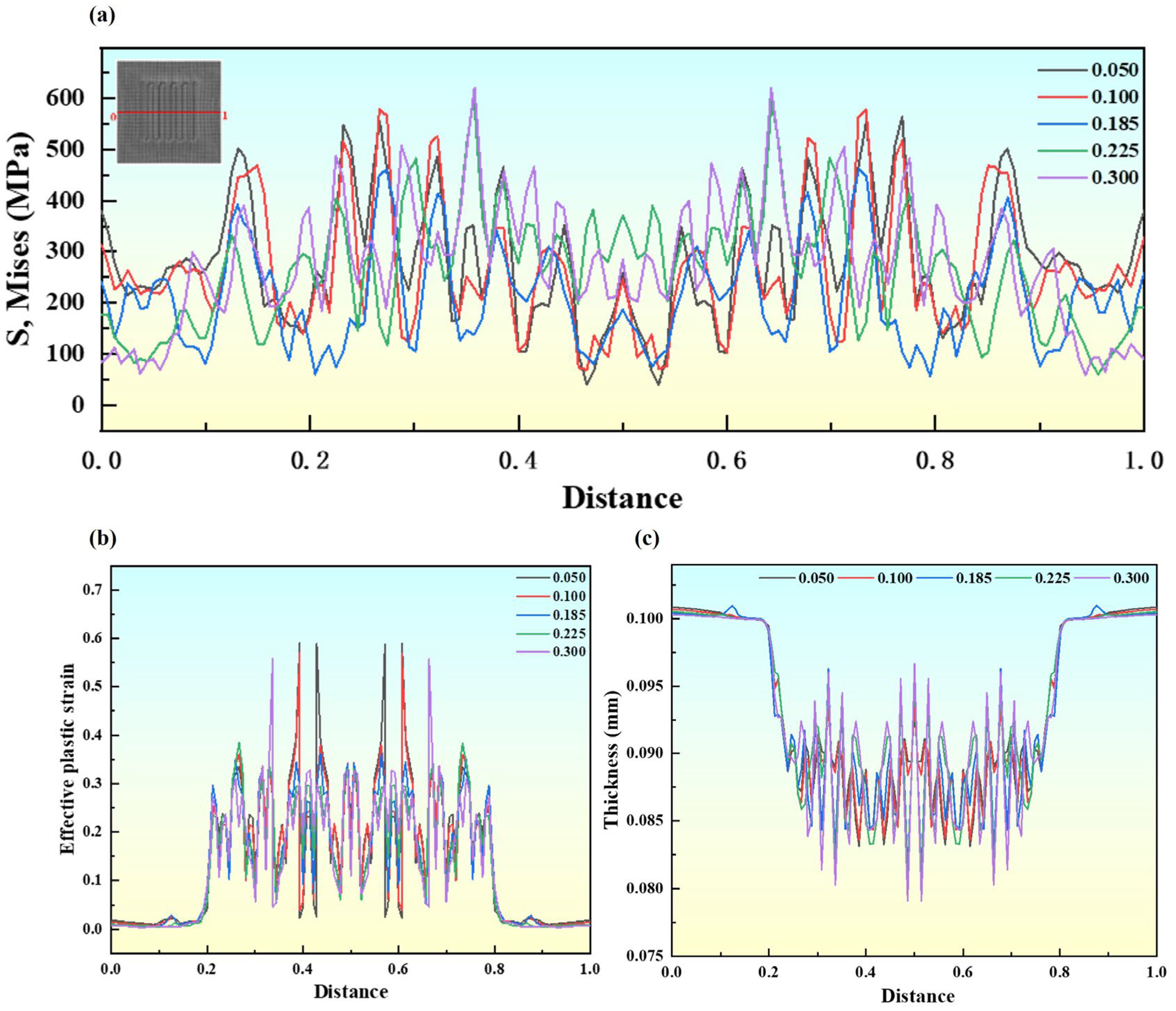
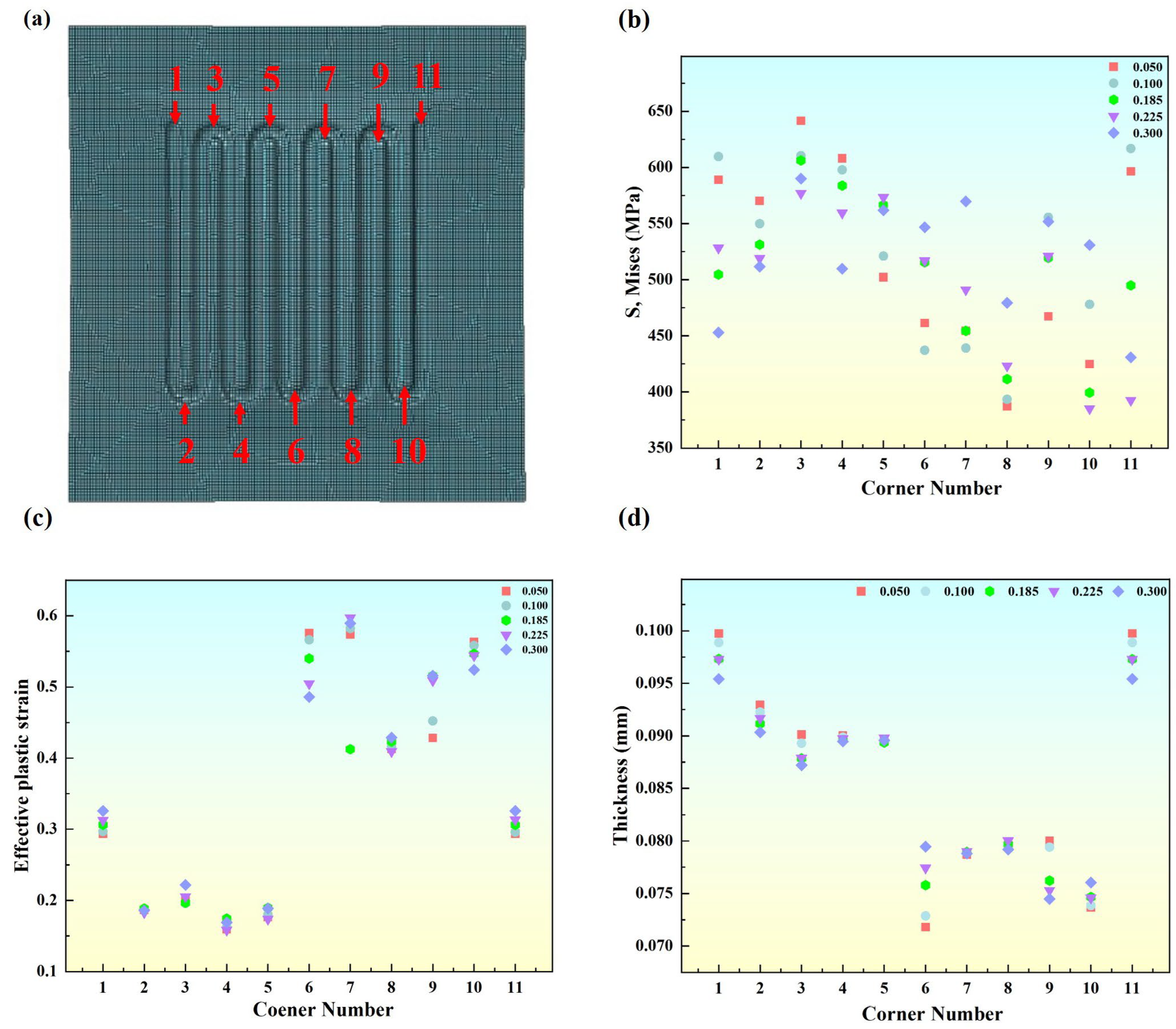
3.2. The Influence of Friction Coefficient on the Forming Quality
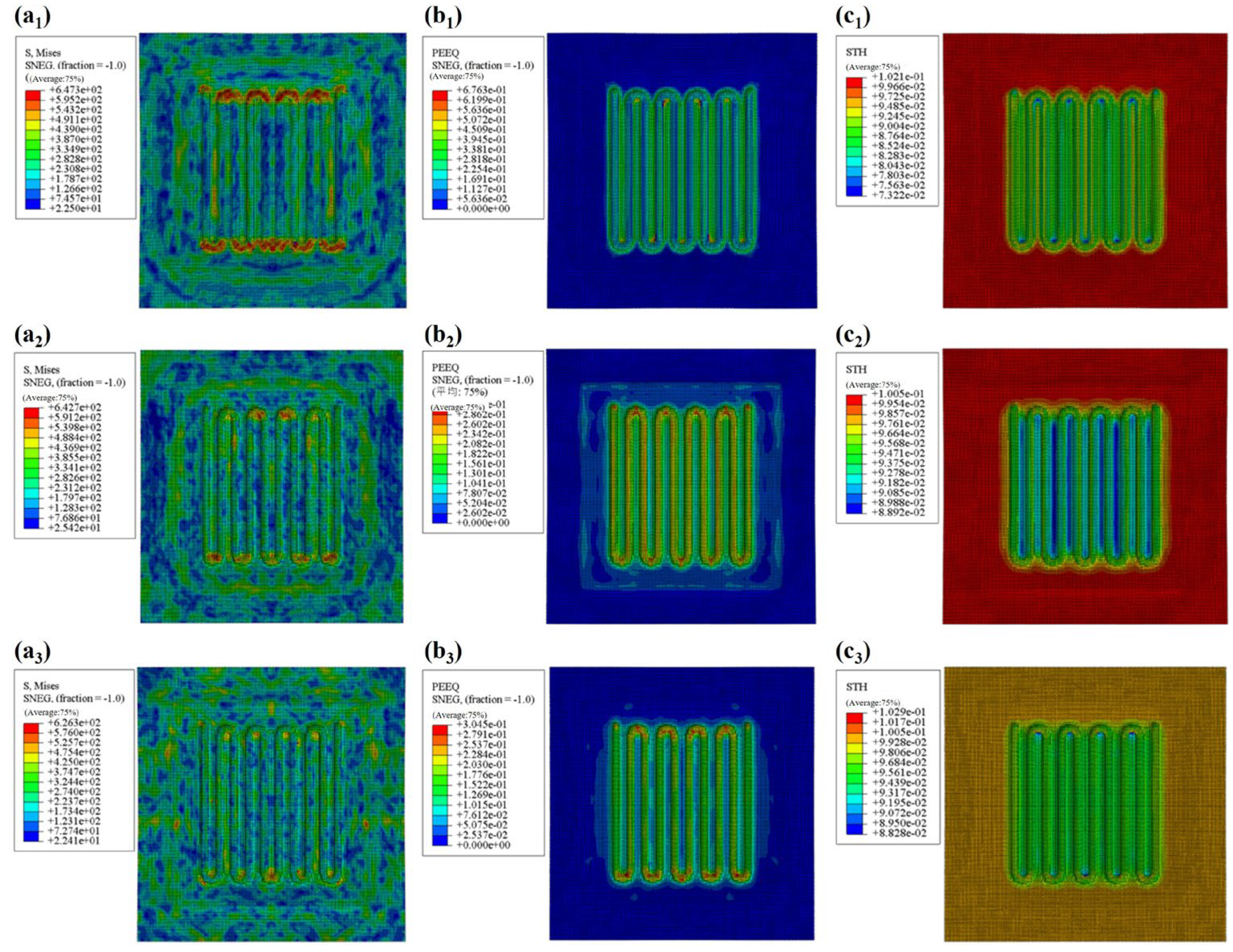
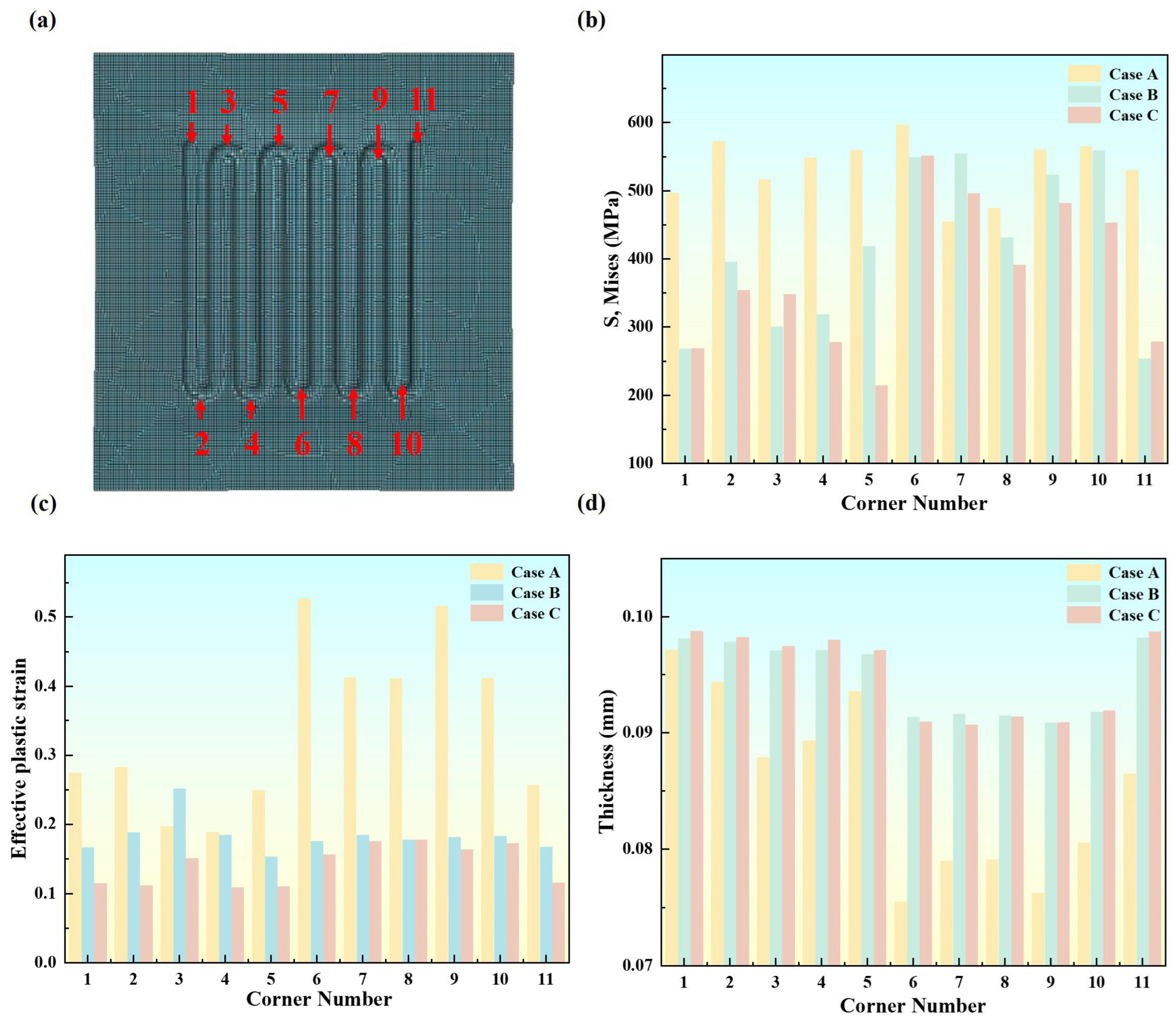
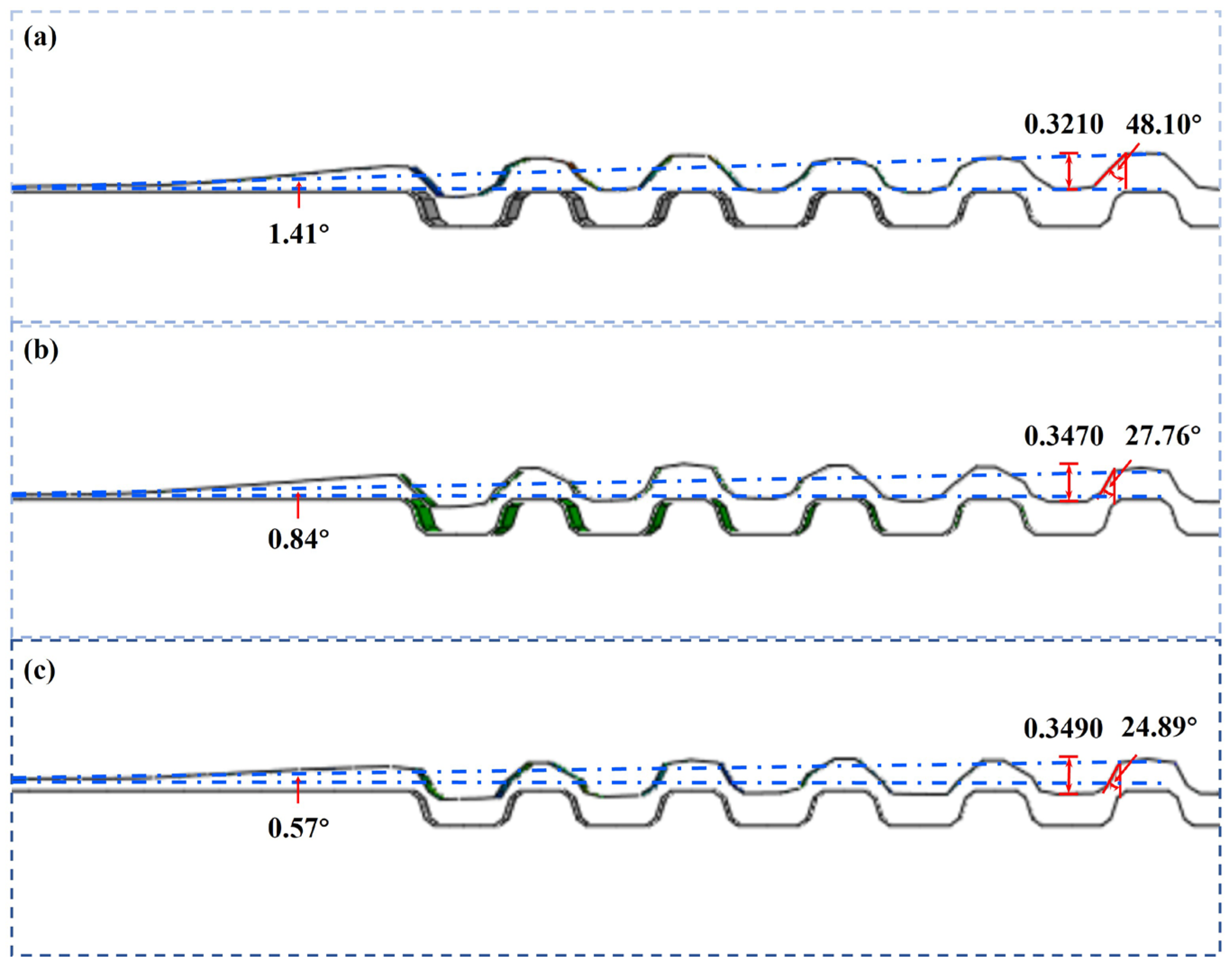
3.3. The Influence of Stamping Method on the Forming Quality
4. Conclusions
- (1)
- Process parameters play a critical role in the forming quality of BPs. At a stamping speed of 100 mm/s and a friction coefficient of 0.185, the peak stress and strain are 647.3 MPa and 6.76%, respectively, with a thickness-reduction rate of 26.8%. This enables optimal material flow and die conformity, uniform stress distribution, and effective control of strain and thickness reduction. Proper matching of stamping speed and friction coefficient is key to improving forming quality.
- (2)
- In terms of stamping methods, the optimized two-stage stamping process outperforms both the single-stage and traditional two-stage processes across multiple indicators. Regarding maximum stress, the optimized process reduces the inner fillet stress from 642.7 MPa (traditional process) to 626.3 MPa; the maximum strain decreases from 3.12% to 3.04%; and the maximum thickness reduction rate significantly drops to 10.2%. Additionally, in terms of forming accuracy, the optimized process achieves a channel depth of 0.349 mm and a channel angle of 24.89°, which are far superior to those obtained with the single-stage and traditional two-stage processes. The warpage angle is minimized to just 0.57°, greatly enhancing dimensional consistency and springback control.
Author Contributions
Funding
Data Availability Statement
Conflicts of Interest
References
- Lohse-busch, H.; Stutenberg, K.; Duoba, M.; Liu, X.; Elgowainy, A.; Wang, M.; Wallner, T.; Richard, B.; Christenson, M. ScienceDirect Automotive Fuel Cell Stack and System Efficiency and Fuel Consumption Based on Vehicle Testing on a Chassis Dynamometer at Minus 18 °C to Positive 35 °C Temperatures. Int. J. Hydrogen Energy 2019, 45, 861–872. [Google Scholar] [CrossRef]
- Olabi, A.G.; Wilberforce, T.; Alanazi, A.; Vichare, P.; Sayed, E.T.; Maghrabie, H.M.; Elsaid, K.; Abdelkareem, M.A. Novel Trends in Proton Exchange Membrane Fuel Cells. Energies 2022, 15, 4949. [Google Scholar] [CrossRef]
- Yu, X.; Chang, H.; Zhao, J.; Tu, Z.; Chan, S.H. Application of Self-Adaptive Temperature Recognition in Cold-Start of an Air-Cooled Proton Exchange Membrane Fuel Cell Stack. Energy AI 2022, 9, 100155. [Google Scholar] [CrossRef]
- Xu, Z.; Li, Z.; Zhang, R.; Jiang, T.; Peng, L. Fabrication of Micro Channels for Titanium PEMFC Bipolar Plates by Multistage Forming Process. Int. J. Hydrogen Energy 2021, 46, 11092–11103. [Google Scholar] [CrossRef]
- Wang, X.Z.; Fan, H.Q.; Muneshwar, T.; Cadien, K.; Luo, J.L. Balancing the Corrosion Resistance and Through-Plane Electrical Conductivity of Cr Coating via Oxygen Plasma Treatment. J. Mater. Sci. Technol. 2021, 61, 75–84. [Google Scholar] [CrossRef]
- Tran, M.T.; Lee, D.H.; Lee, H.W.; Kim, D.K. Formability Improvement in Multi-Stage Stamping of Ultra-Thin Metallic Bipolar Plate for Proton Exchange Membrane Fuel Cell. Int. J. Hydrogen Energy 2022, 47, 40008–40025. [Google Scholar] [CrossRef]
- Elferjani, I.; Serre, G.; Ter-Ovanessian, B.; Normand, B. A Coupling Approach between Metallic Bipolar Plates Corrosion and Membrane Chemical Degradation in the Proton Exchange Membrane Fuel Cells. Int. J. Hydrogen Energy 2021, 46, 32226–32241. [Google Scholar] [CrossRef]
- Bong, H.J.; Lee, J.; Kim, J.H.; Barlat, F.; Lee, M.G. Two-Stage Forming Approach for Manufacturing Ferritic Stainless Steel Bipolar Plates in PEM Fuel Cell: Experiments and Numerical Simulations. Int. J. Hydrogen Energy 2017, 42, 6965–6977. [Google Scholar] [CrossRef]
- Chen, T.C.; Ye, J.M. Fabrication of Micro-Channel Arrays on Thin Stainless Steel Sheets for Proton Exchange Membrane Fuel Cells Using Micro-Stamping Technology. Int. J. Adv. Manuf. Technol. 2013, 64, 1365–1372. [Google Scholar] [CrossRef]
- Hu, Q.; Zhang, D.; Fu, H.; Huang, K. Investigation of Stamping Process of Metallic Bipolar Plates in PEM Fuel Cell—Numerical Simulation and Experiments. Int. J. Hydrogen Energy 2014, 39, 13770–13776. [Google Scholar] [CrossRef]
- Modanloo, V.; Alimirzaloo, V.; Elyasi, M. Optimal Design of Stamping Process for Fabrication of Titanium Bipolar Plates Using the Integration of Finite Element and Response Surface Methods. Arab. J. Sci. Eng. 2020, 45, 1097–1107. [Google Scholar] [CrossRef]
- Zhao, Y.; Peng, L. Formability and Flow Channel Design for Thin Metallic Bipolar Plates in PEM Fuel Cells: Modeling. Int. J. Energy Res. 2019, 43, 2592–2604. [Google Scholar] [CrossRef]
- Neto, D.M.; Oliveira, M.C.; Alves, J.L.; Menezes, L.F. Numerical Study on the Formability of Metallic Bipolar Plates for Proton Exchange Membrane (PEM) Fuel Cells. Metals 2019, 9, 810. [Google Scholar] [CrossRef]
- Zhang, H. Research on Stamping of SS316L Metal Bipolar Plates for Proton Exchange Membrane Fuel Cells. Master’s Thesis, Taiyuan University of Technology, Taiyuan, China, 2022. [Google Scholar]
- Liu, Y.; Hua, L.; Lan, J.; Wei, X. Studies of the Deformation Styles of the Rubber-Pad Forming Process Used for Manufacturing Metallic Bipolar Plates. J. Power Sources 2010, 195, 8177–8184. [Google Scholar] [CrossRef]
- Mohammadtabar, N.; Bakhshi-Jooybari, M.; Hosseinipour, S.J.; Gorji, A.H. Feasibility Study of a Double-Step Hydroforming Process for Fabrication of Fuel Cell Bipolar Plates with Slotted Interdigitated Serpentine Flow Field. Int. J. Adv. Manuf. Technol. 2016, 85, 765–777. [Google Scholar] [CrossRef]
- Lee, K.H.; Jin, C.K.; Kang, C.G.; Seo, H.Y.; Kim, J.D. Fabrication of Titanium Bipolar Plates by Rubber Forming Process and Evaluation Characteristics of TiN Coated Titanium Bipolar Plates. Fuel Cells 2015, 15, 170–177. [Google Scholar] [CrossRef]
- Wang, S.; Wu, Y.; Xu, Q.; Ma, Y.; Wang, T. Research on Stamping Formability and Process Simulation of AZ31 Magnesium Alloy Based on Deep Learning. Mater. Today Commun. 2024, 40, 109807. [Google Scholar] [CrossRef]
- Zhu, S.; Ding, Y.; Long, B.; Guo, H.; Ouyang, L.; Chen, W.; Jiang, Z. Analysis and Optimization of Stamping and Forming Process of Bearing Outer Ring. Theor. Appl. Mech. Lett. 2024, 14, 100522. [Google Scholar] [CrossRef]
- Yang, X.; Wang, B.; Zhou, J.; Dang, L.; Xiao, W.; Wang, Y. Influence of Process Parameters on Deep Drawing of 2060 Al–Li Alloy Under Hot Stamping Process. Int. J. Light. Mater. Manuf. 2020, 3, 36–42. [Google Scholar] [CrossRef]
- Smith, T.L.; Santamaria, A.D.; Park, J.W.; Yamazaki, K. Alloy Selection and Die Design for Stamped Proton Exchange Membrane Fuel Cell (PEMFC) Bipolar Plates. Procedia CIRP 2014, 14, 275–280. [Google Scholar] [CrossRef]
- He, S.; Sun, Y.; Zhang, J.; Tang, Z.; Yan, G.; Zhao, J.; Qin, S. Research on Multi-Stage Deep Drawing with Electro-Permanent Magnet Technology. J. Manuf. Process. 2023, 108, 373–383. [Google Scholar] [CrossRef]
- Derazkola, H.A.; Garcia, E.; Murillo-Marrodán, A. Effects of Skew Rolling Piercing Process Friction Coefficient on Tube Twisting, Strain Rate and Forming Velocity. J. Mater. Res. Technol. 2023, 25, 7254–7272. [Google Scholar] [CrossRef]
- Liang, Y.F.; Chen, Z.F.; Wang, W.; Wang, C.Y. The Effect of Friction Coefficient on Wrinkles of Lined Pipe Under Bending. Int. J. Solids Struct. 2024, 288, 112615. [Google Scholar] [CrossRef]
- Yang, X.; Liu, H.; Wu, V.; Politis, D.J.; Yao, H.; Zhang, J.; Wang, L. Digitally Enhanced Development of Customised Lubricant: Experimental and Modelling Studies of Lubricant Performance for Hot Stamping. Comput. Ind. 2024, 163, 104152. [Google Scholar] [CrossRef]
- Khatir, F.A.; Elyasi, M.; Ghadikolaee, H.T.; Hosseinzadeh, M. Evaluation of Effective Parameters on Stamping of Metallic Bipolar Plates. Procedia Eng. 2017, 183, 322–329. [Google Scholar] [CrossRef]
- Zhong, Q.; Hua, R.; Wang, C.; Cheng, L.; Ma, Z.; He, H.; Chen, F. Investigation on Three-Stage Stamping of Micro-Channels with Titanium Ultra-Thin Sheet Used for PEM Fuel Cell Bipolar Plates. Int. J. Adv. Manuf. Technol. 2023, 127, 1377–1389. [Google Scholar] [CrossRef]
- Zhang, J.; Chen, Z.; Zhang, H.; Zeng, Y.; Zhang, X. Investigation of Roll Forming Process and Quality Control Factors for Metal Bipolar Plates. Int. J. Hydrogen Energy 2024, 93, 898–909. [Google Scholar] [CrossRef]
- Joo Tan, C. Multi-Stage Stamping of Lightweight Steel Wheel Disks by Controlling Its Wall Thickness Distribution. In Encyclopedia of Renewable and Sustainable Materials; Elsevier Ltd.: Amsterdam, The Netherlands, 2020; Volume 1–5, ISBN 9780128131961. [Google Scholar]


| Element | C | Mn | Si | P | S | Cr | Ni | Fe |
|---|---|---|---|---|---|---|---|---|
| wt.% | ≤0.10 | ≤0.10 | ≤1.00 | ≤0.04 | ≤0.03 | 16~18 | ≤0.75 | Bal. |
| Microchannel Depth h (mm) | Corner Radius r (mm) | Pattern Draft α (°) | |
|---|---|---|---|
| 1 | 0.30 | 0.1050 | 19.50 |
| 2 | 0.32 | 0.1075 | 19.75 |
| 3 | 0.35 | 0.1100 | 20.00 |
| 4 | 0.38 | 0.1125 | 20.25 |
| 5 | 0.40 | 0.1150 | 20.50 |
| Estimate | SE | tstat | P | |
|---|---|---|---|---|
| Constant | 5.7503 | 21.416 | 0.2685 | 0.79197 |
| h | 11.453 | 9.0626 | 1.2638 | 0.22559 |
| r | −118.17 | 131.94 | −0.89566 | 0.38458 |
| α | −0.10142 | 1.9853 | −0.051084 | 0.0002 |
| hr | −29.726 | 39.704 | −0.74869 | 0.95993 |
| hα | −0.36905 | 0.39084 | −0.94424 | 0.46562 |
| rα | 5.0685 | 4.1665 | 1.2165 | 0.36001 |
| h2 | 0.86809 | 5.0194 | 0.17295 | 0.24259 |
| r2 | 114.86 | 447.64 | 0.2566 | 0.865 |
| α2 | −0.0085596 | 0.048097 | −0.17797 | 0.86113 |
| RMSE | 0.0233 | |||
| R2 | 0.898 | |||
| F-statistic | 14.6 | p | 6.62 × 10⁶ | |
| Estimate | SE | tstat | P | |
|---|---|---|---|---|
| Constant | −28,587 | 42,647 | 0.67033 | 0.51284 |
| h | 2620.9 | 18,046 | 0.14523 | 0.88646 |
| r | 148,090 | 262,720 | 0.56368 | 0.5813 |
| α | 1995.5 | 3953.4 | 0.50476 | 0.62106 |
| hr | 19,094 | 79,062 | 0.24154 | 0.81243 |
| hα | −875.52 | 778.28 | −1.1249 | 0.27829 |
| rα | −1137.9 | 8296.7 | −0.13715 | 0.89273 |
| h2 | 17,711 | 9995 | 1.772 | 0.096704 |
| r2 | −581,540 | 891,390 | −0.6524 | 0.52402 |
| α2 | −38.055 | 95.775 | −0.39773 | 0.6967 |
| RMSE | 46.4 | |||
| R2 | 0.464 | |||
| F-statistic | 1.44 | p | 0.255 | |
Disclaimer/Publisher’s Note: The statements, opinions and data contained in all publications are solely those of the individual author(s) and contributor(s) and not of MDPI and/or the editor(s). MDPI and/or the editor(s) disclaim responsibility for any injury to people or property resulting from any ideas, methods, instructions or products referred to in the content. |
© 2025 by the authors. Licensee MDPI, Basel, Switzerland. This article is an open access article distributed under the terms and conditions of the Creative Commons Attribution (CC BY) license (https://creativecommons.org/licenses/by/4.0/).
Share and Cite
Lan, J.; Han, J.; Zhu, L.; Song, J.; Meng, M.; Jiang, Z. Optimization of Forming Parameters and Forming Strategy for Stamping of Novel Ultra-Thin Super Ferritic Stainless Steel Bipolar Plates Based on Numerical Simulation. Metals 2025, 15, 620. https://doi.org/10.3390/met15060620
Lan J, Han J, Zhu L, Song J, Meng M, Jiang Z. Optimization of Forming Parameters and Forming Strategy for Stamping of Novel Ultra-Thin Super Ferritic Stainless Steel Bipolar Plates Based on Numerical Simulation. Metals. 2025; 15(6):620. https://doi.org/10.3390/met15060620
Chicago/Turabian StyleLan, Jun, Jian Han, Lisong Zhu, Jingwen Song, Meiqing Meng, and Zhengyi Jiang. 2025. "Optimization of Forming Parameters and Forming Strategy for Stamping of Novel Ultra-Thin Super Ferritic Stainless Steel Bipolar Plates Based on Numerical Simulation" Metals 15, no. 6: 620. https://doi.org/10.3390/met15060620
APA StyleLan, J., Han, J., Zhu, L., Song, J., Meng, M., & Jiang, Z. (2025). Optimization of Forming Parameters and Forming Strategy for Stamping of Novel Ultra-Thin Super Ferritic Stainless Steel Bipolar Plates Based on Numerical Simulation. Metals, 15(6), 620. https://doi.org/10.3390/met15060620