
Research on Unidirectional Traveling Wire Electrochemical Discharge Micromachining of Thick Metal Materials


Abstract
1. Introduction
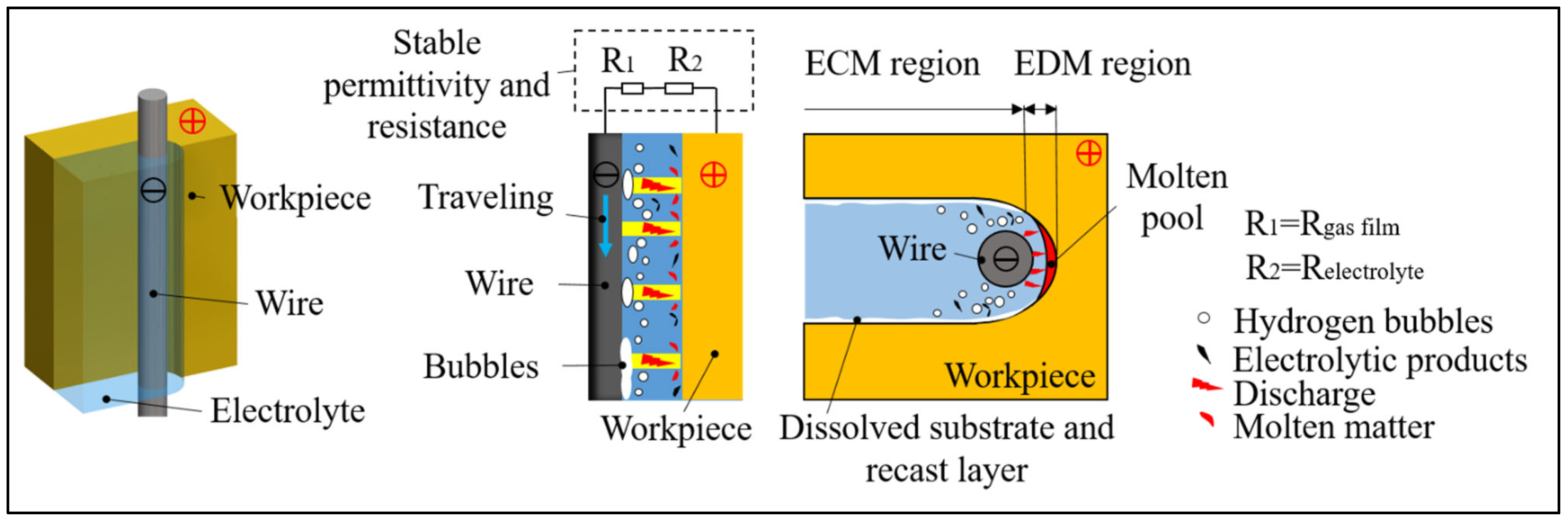
2. Principle of UWECDMM
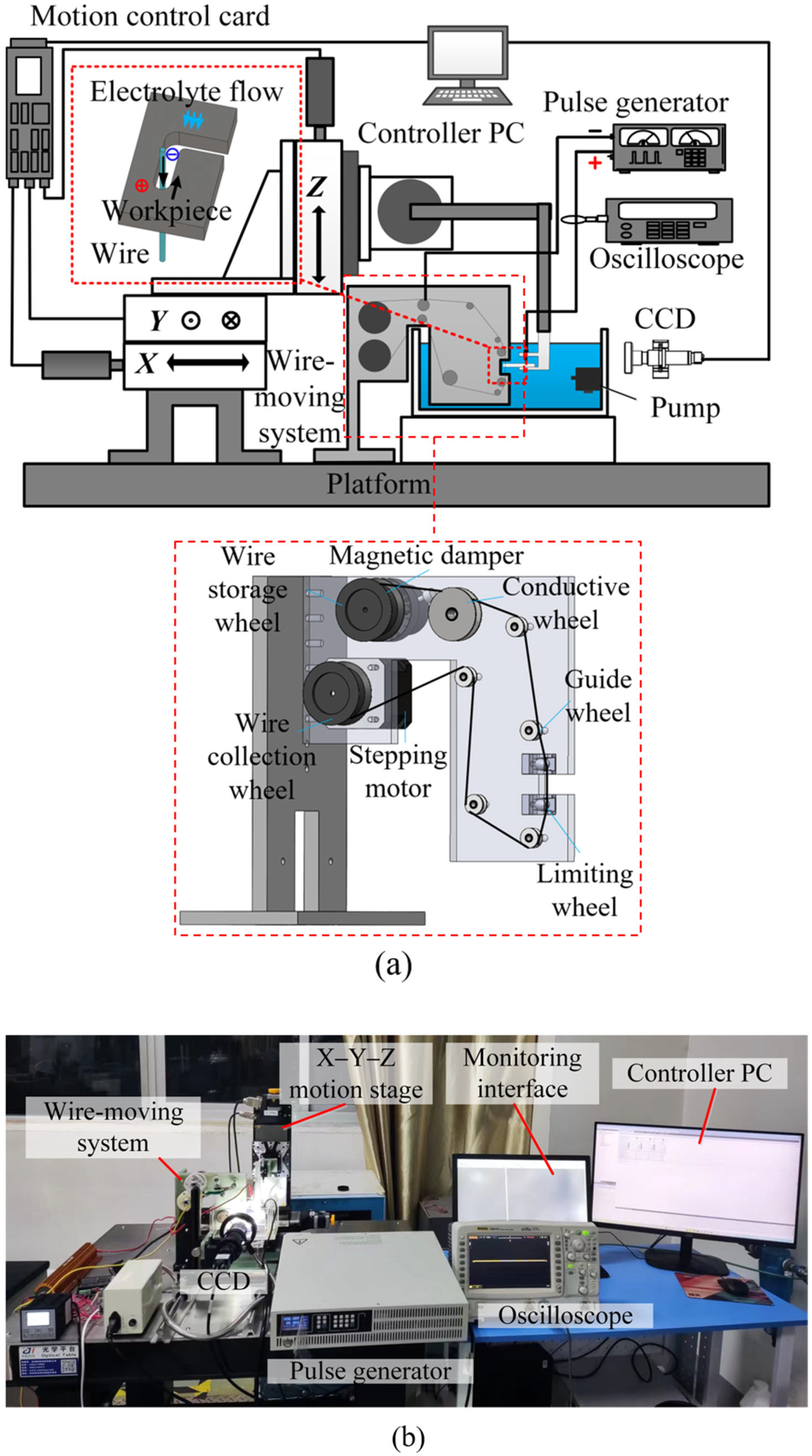
3. Experimental System and Methods
4. Results
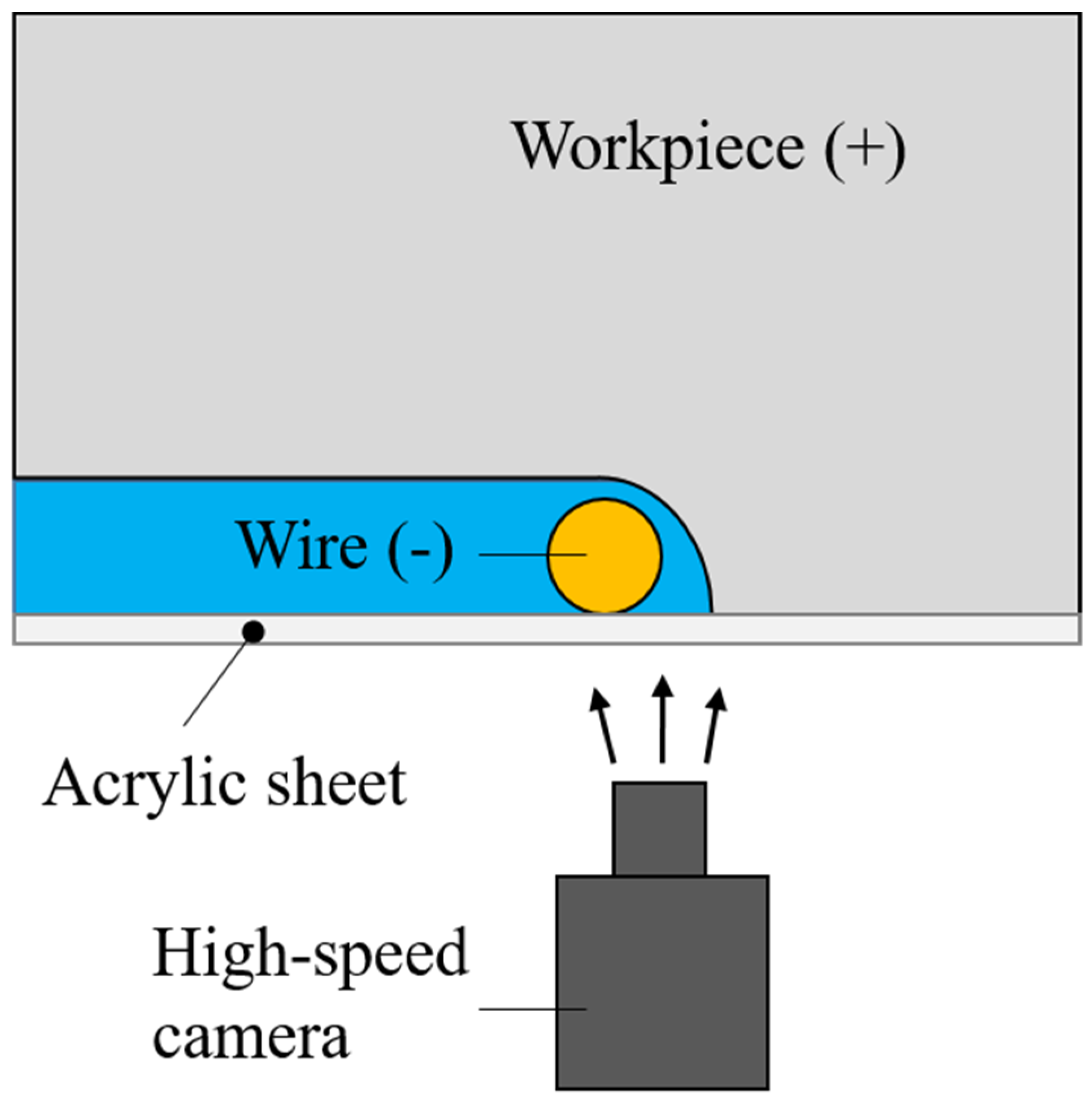
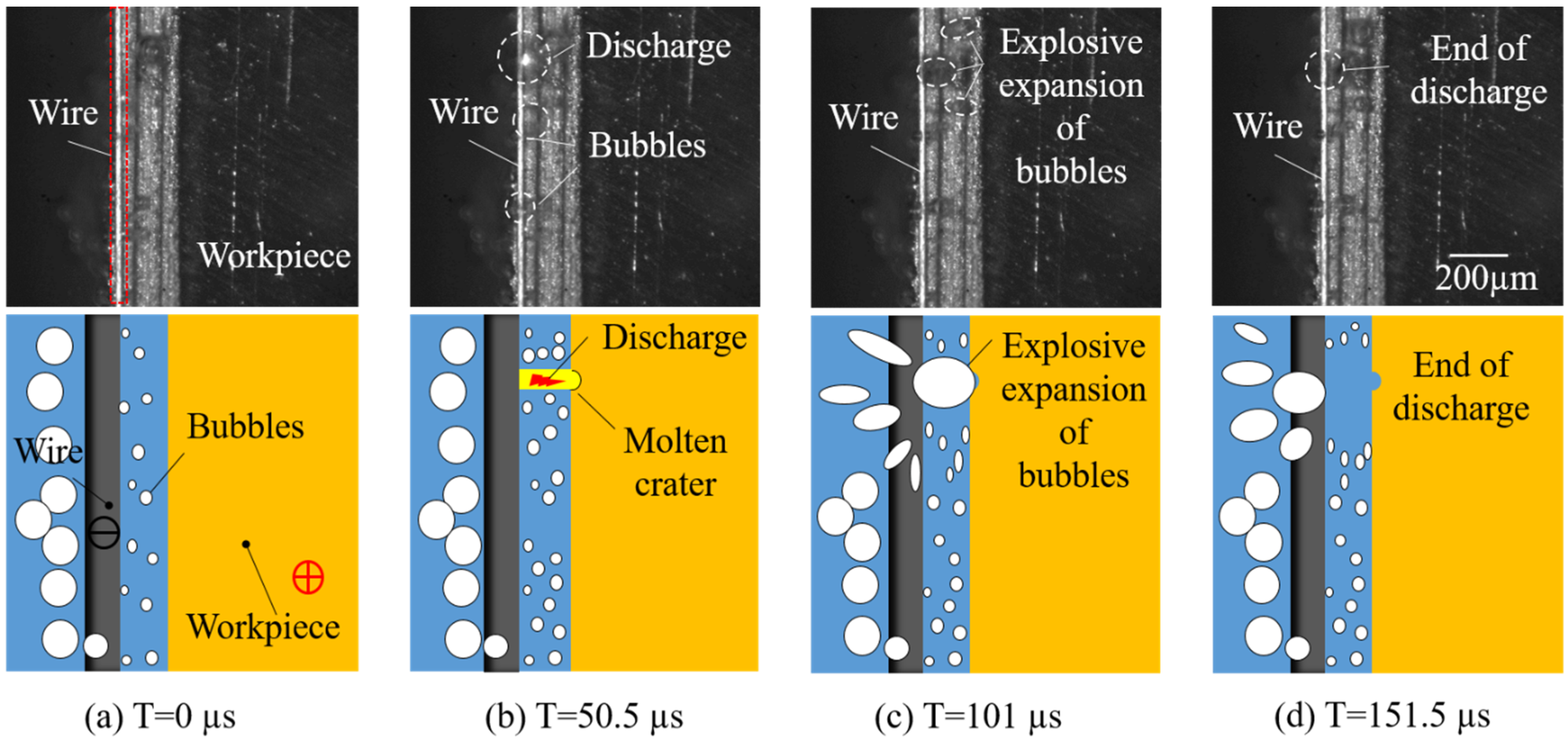
4.1. Observation of Discharge
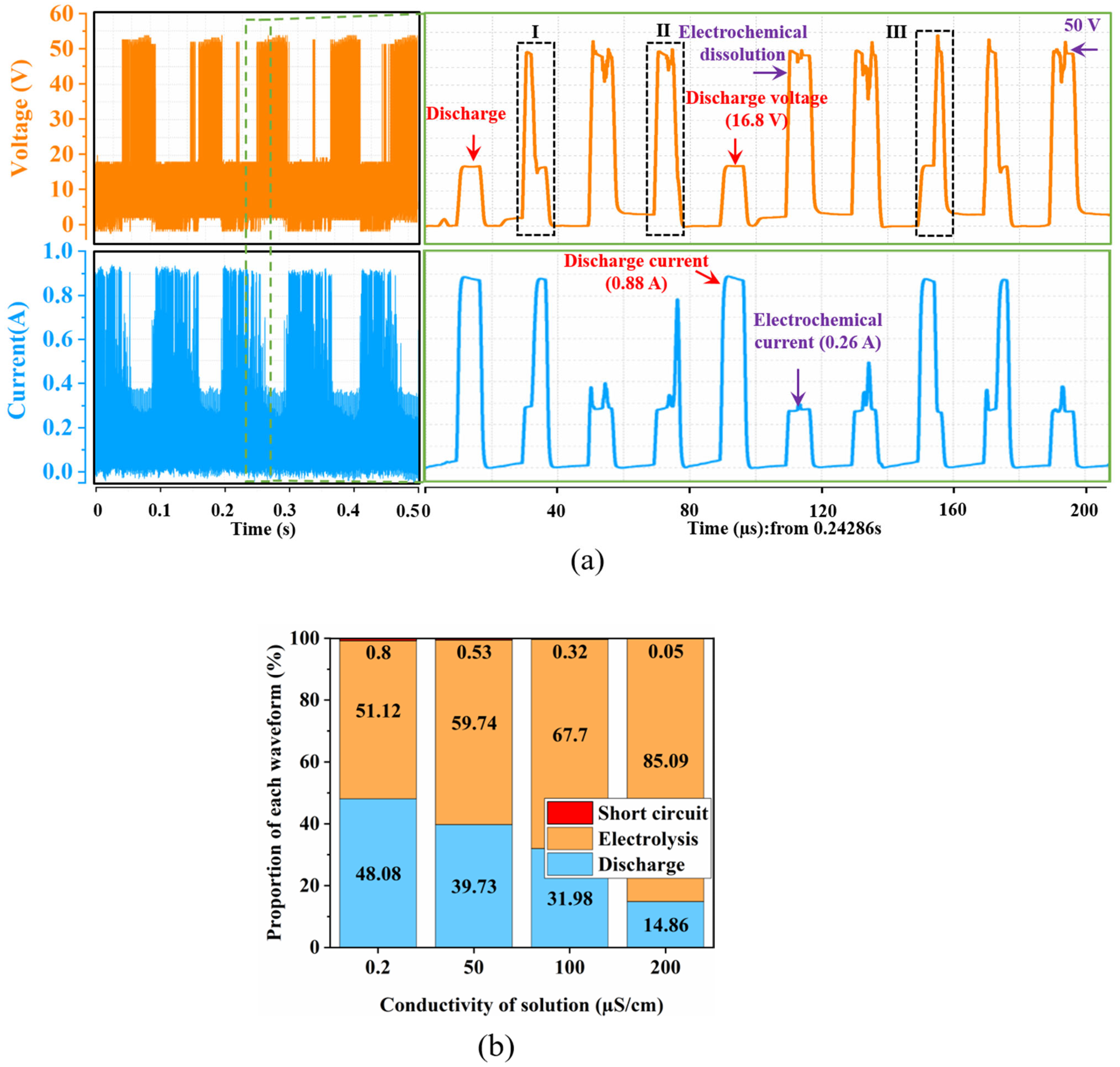
4.2. Analysis of Processed Waveforms
4.3. The Influence of Process Parameters on Machining
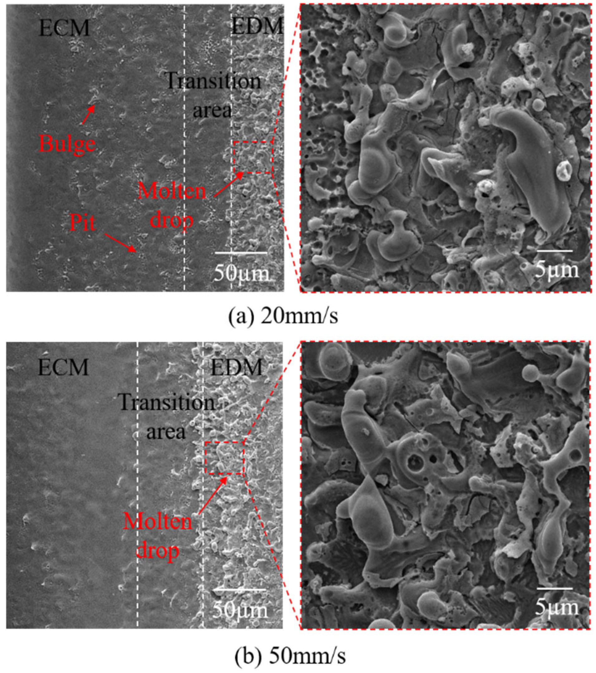
4.3.1. Characteristics of Processed Surfaces
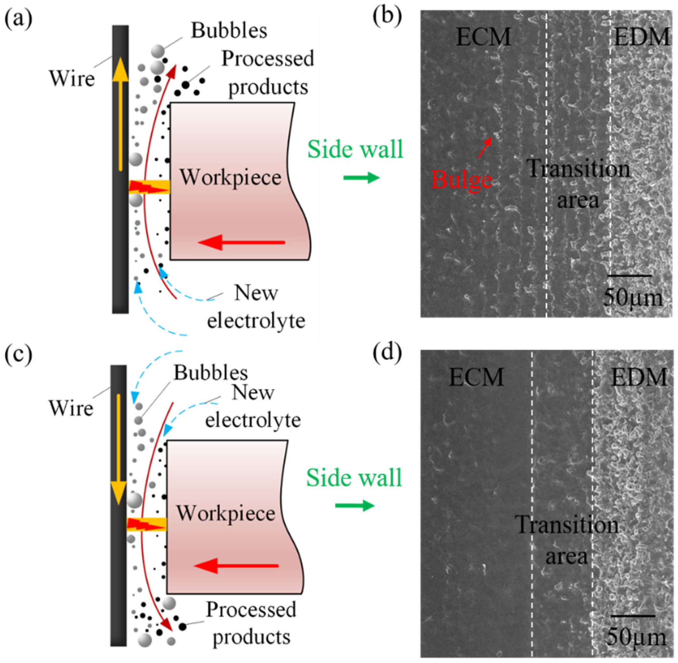
4.3.2. The Direction and Speed of the Traveling Wire
4.3.3. Slit Width
5. Discussion
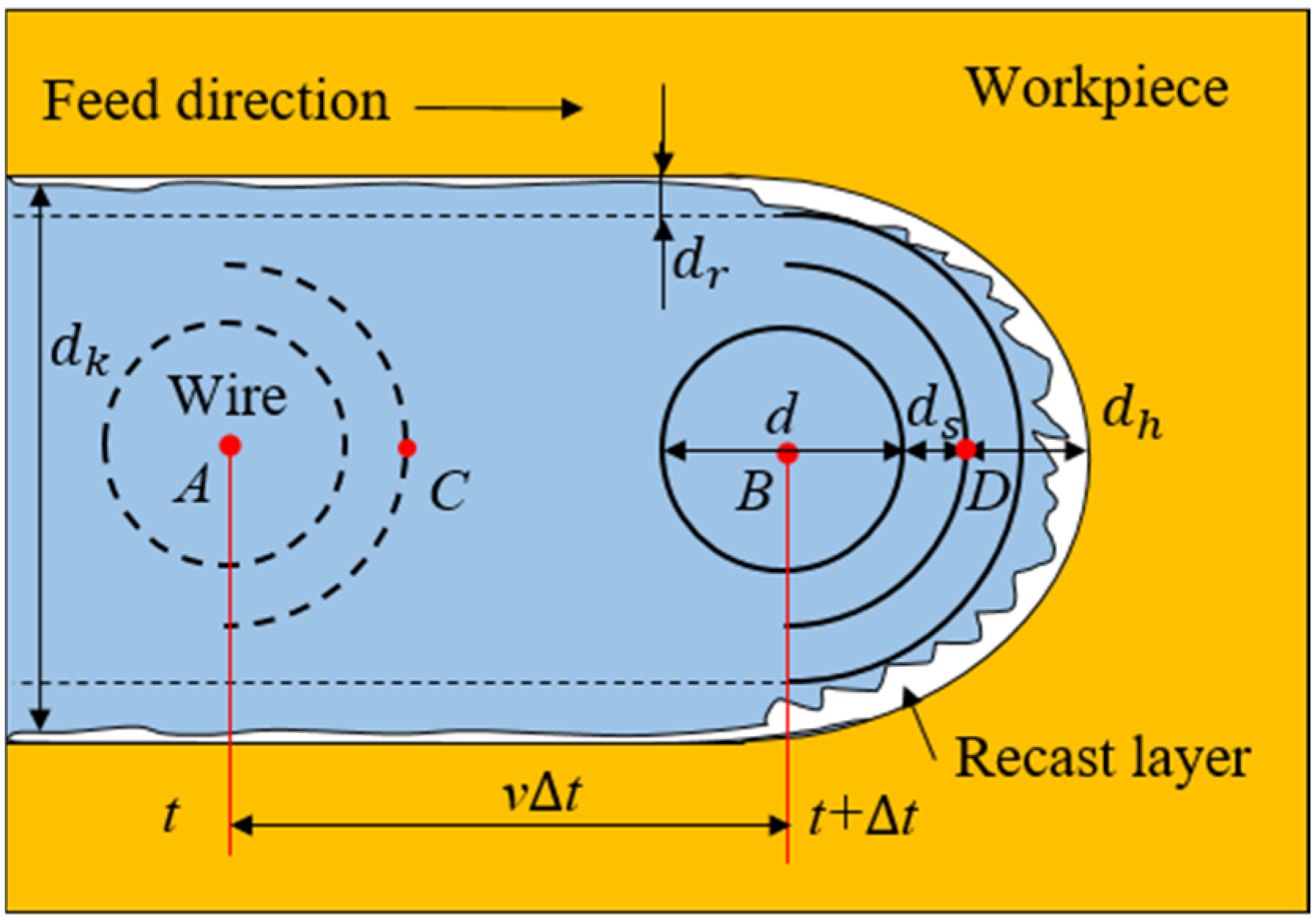
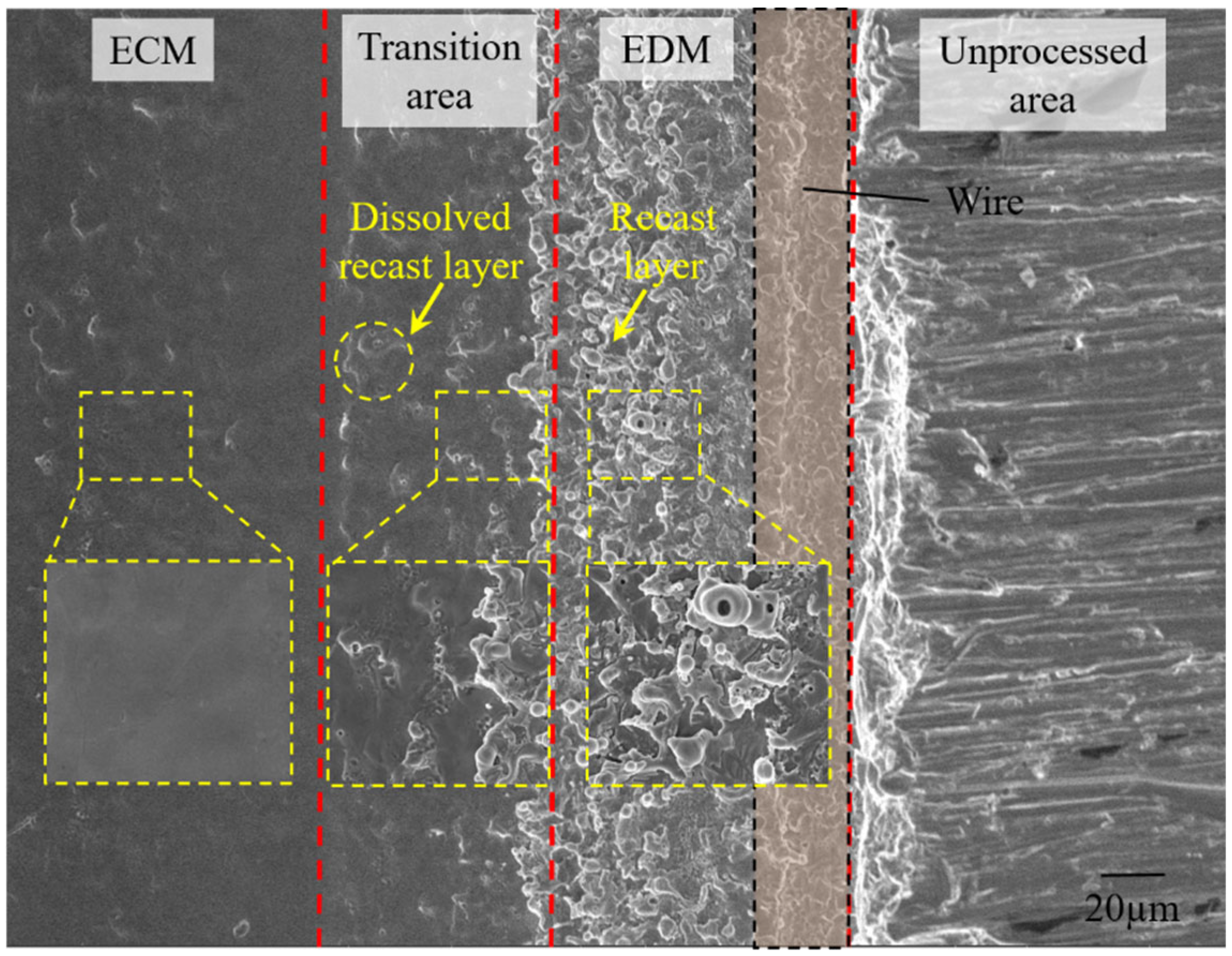
5.1. Removal of Recast Layer and Evolution of Surface Morphology
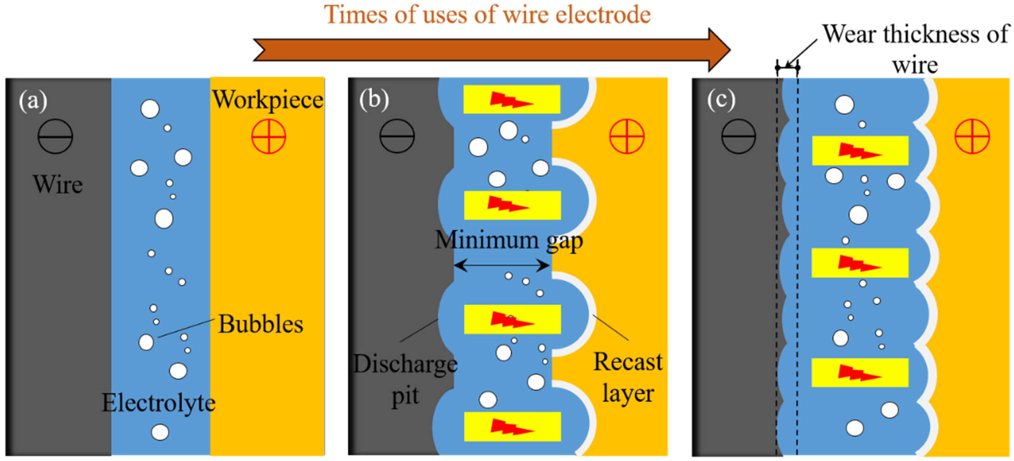
5.2. Analysis of Wear of Wire Electrode
5.3. Typical Microstructure Processing
6. Conclusions
- The discharge phenomenon of UWECDMM was directly observed through a high-speed camera. The results show that the discharge is mainly breakdown electrolyte discharge at low conductivity. Waveform analysis shows that ECM and EDM alternate, and as the electrolyte conductivity increases, the discharge proportion decreases from 48.08% to 14.86%. The discharge current is less than 1 A (0.88 A), and the discharge energy is small, which is conducive to high-precision machining of microstructures.
- There is no significant difference in the morphology between the upward and downward traveling wires in the EDM area. However, in the ECM area, the surface of the upward traveling wire exhibits numerous bulges, while the bulges on the surface of the downward traveling wire are significantly reduced, resulting in higher surface quality. Additionally, the surface quality of the high-speed traveling wire is superior to that of the low-speed traveling wire.
- After discharge, a recast layer was formed on the machined surface. When the conductivity of the electrolyte is 200 μS/cm, the recast layer on the side wall of the slit is completely dissolved, achieving processing without a recast layer, and the surface roughness is only Ra 0.06 μm.
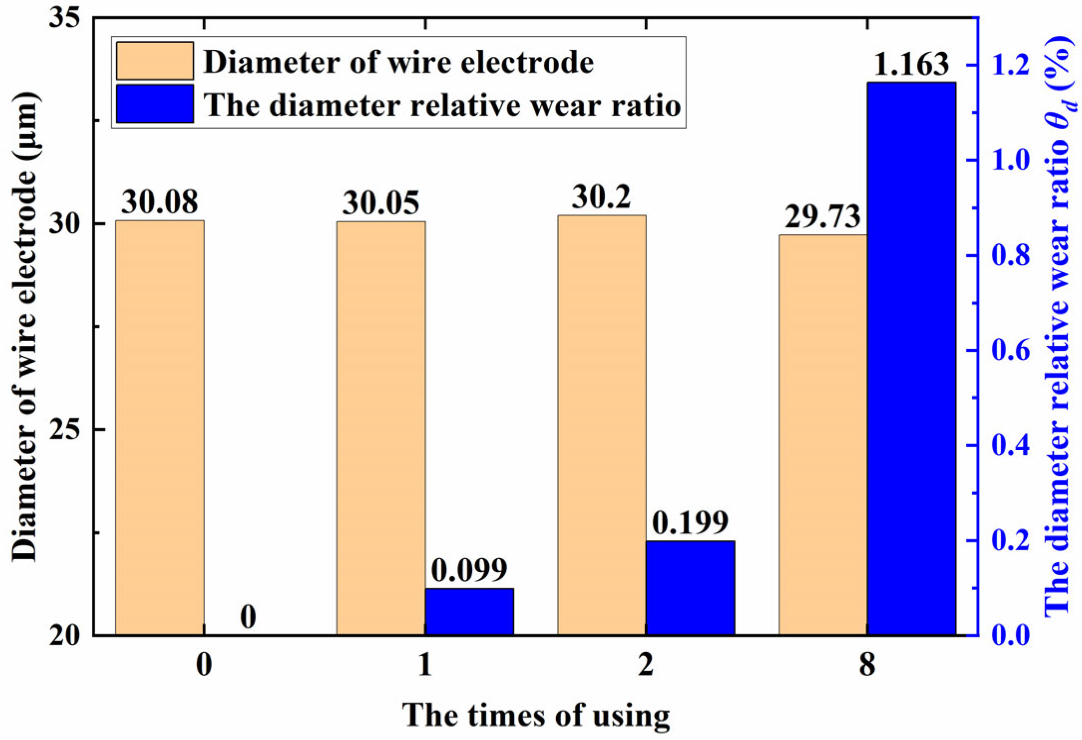
- After multiple uses, the surface discharge pits of the tungsten wire increased, but the diameter did not significantly decrease. After eight uses, the relative loss rate of the diameter was only 1.163%, and it was still able to obtain high-quality non-recast-layer machined surfaces. Reducing experimental costs is in line with the concept of sustainable development.
- By using optimized process parameters to process typical microstructures, the surface roughness was only Ra 0.06 μm, and the depth diameter ratio could reach 200. By processing typical microstructures, the feasibility of ethylene glycol-based UWECDMM was verified, providing a method for efficient and high-precision microfabrication of conductive materials.
Author Contributions
Funding
Data Availability Statement
Conflicts of Interest
Nomenclature
| WEDMM | Wire electrical discharge micromachining |
| WECMM | Wire electrochemical micromachining |
| WECDMM | Wire electrochemical discharge micromachining |
| EDM | Electrical discharge machining |
| ECM | Electrochemical machining |
| UWECDMM | Unidirectional traveling wire electrochemical discharge micromachining |
| M | The mass of metal dissolved at the anode (g) |
| k | The mass of dissolved elements per unit of electricity [g/(A·s)] |
| Q | The amount of electricity passing through the two-phase interface (A·s) |
| I | The current intensity (A) |
| t | The time for the current to pass through (s) |
| The proportion of electrolytic pulses in the machining process (%) | |
| The material volume dissolved by electrolysis (mm3) | |
| The volume of the recast layer at time t + (mm3) | |
| The total volume of the recast layer within time (mm3) | |
| The pulse period (s) | |
| The pulse width (s) | |
| d | The diameter of electrode wire (µm) |
| l | The thickness of the workpiece (mm) |
| ω | The volume electrochemical equivalent of the element (cm3/C) |
| The electrochemical reaction current density (A/m2) | |
| v | The feed rate of electrode wire (µm/s) |
| The discharge gap (µm) | |
| The thickness of the recast layer (µm) | |
| The depth of the discharge pit (µm) | |
| The width of the slit (µm) | |
| N | The total number of recast layers generated during ∆t time |
| δ | The coefficient of electrolytic dissolution |
References
- Liu, Y.; Ouyang, P.; Zhang, Z.; Xue, W.; Wang, Y. Multi-energy field simulation and experimental research on backside water assisted laser processing for thin-walled irregular metal micro-holes. Opt. Laser Technol. 2025, 187, 112790. [Google Scholar] [CrossRef]
- Zhu, H.; Xie, W.; Du, W.; Zhang, Q.; Yuan, H.; Xu, K.; Liu, Y.; Wang, J.; Saetang, V.; Zhang, Z. Fabrication and quality improvement of film cooling holes via picosecond laser drilling assisted by waterjet and post-electrochemical machining. Opt. Laser Technol. 2025, 182, 112162. [Google Scholar] [CrossRef]
- Zhu, D.; Wang, K.; Qu, N. Micro Wire Electrochemical Cutting by Using In Situ Fabricated Wire Electrode. CIRP Ann. 2007, 56, 241–244. [Google Scholar] [CrossRef]
- Wang, J.; Zhang, J.; Zhang, Z.; Zhu, H.; Xu, K.; Liu, Y.; Xue, W.; Li, T. Anodic dissolution and passivation mechanisms of 07Cr16Ni6 in K3Cit solution and its electrochemical machining for microstructure. Corros. Sci. 2025, 250, 112877. [Google Scholar] [CrossRef]
- Wang, J.; Wang, Y.; Shi, X.; Ouyang, P.; Zhang, Z.; Zhu, H.; Xu, K.; Liu, Y. Anodic dissolution behavior and microstructure preparation of nickel based superalloy in cryogenic-shielded and laser-assisted electrochemical machining. J. Mater. Process. Technol. 2025, 338, 118777. [Google Scholar] [CrossRef]
- Liu, Y.; Wang, H.; Zhang, Z.; Zhu, H.; Song, J. Laser-chemical composite manufacturing of biomimetic stepped armor functional metal surface with wear resistance and anti-icing characteristics. J. Colloid Interface Sci. 2025, 685, 49–62. [Google Scholar] [CrossRef] [PubMed]
- Abbas, N.M.; Solomon, D.G.; Bahari, M.F. A review on current research trends in electrical discharge machining (EDM). Int. J. Mach. Tools Manuf. 2007, 47, 1214–1228. [Google Scholar] [CrossRef]
- Luo, J.; Fang, X.; Yang, T.; Zhu, D. Electrochemical drilling of small holes by regulating in real-time the electrolyte flowrate in multiple channels. Chin. J. Aeronaut. 2022, 35, 470–483. [Google Scholar] [CrossRef]
- Nguyen, M.D.; Rahman, M.; San Wong, Y. Simultaneous micro-EDM and microECM in low-resistivity deionized water. Int. J. Mach. Tools Manuf. 2012, 54, 55–65. [Google Scholar] [CrossRef]
- Kurita, T.; Hattori, M. A study of EDM and ECM/ECM-lapping complex machining technology. Int. J. Mach. Tools Manuf. 2006, 46, 1804–1810. [Google Scholar] [CrossRef]
- Han, M.S.; Min, B.K.; Lee, S.J. Micro-electrochemical discharge cutting of glass using a surface-textured tool. CIRP J. Manuf. Sci. Techno. 2011, 4, 362–369. [Google Scholar] [CrossRef]
- Singh, T.; Dvivedi, A.; Arya, R.K. Fabrication of micro-slits using W-ECDM process with textured wire surface: An experimental investigation on kerf overcut reduction and straightness improvement. Precis. Eng. 2019, 59, 211–223. [Google Scholar] [CrossRef]
- Liu, Y.; Wei, Z.; Wang, M.; Zhang, J. Experimental investigation of micro wire electrochemical discharge machining by using a rotating helical tool. J. Manuf. Process. 2017, 29, 265–271. [Google Scholar] [CrossRef]
- Jain, V.K.; Rao, P.S.; Choudhary, S.K.; Rajurkar, K.P. Experimental investigations into Traveling Wire Electrochemical Spark Machining (TW-ECSM) of composites. J. Eng. Ind. 2016, 113, 75–84. [Google Scholar] [CrossRef]
- Oza, A.D.; Kumar, A.; Badheka, V.; Arora, A. Traveling Wire Electrochemical Discharge Machining (TW-ECDM) of quartz using zinc coated Brass wire: Investigations on material removal rate and kerf width characteristics. Silicon 2019, 11, 2873–2884. [Google Scholar] [CrossRef]
- Sun, Y.; Gong, Y.D.; Wen, X.L.; Yin, G.Q.; Meng, F.T. Micro milling characteristics of LSWEDM fabricated helical and corrugated micro end mill. Int. J. Mech. Sci. 2020, 167, 105277. [Google Scholar] [CrossRef]
- Li, Z.; Tang, J.; Bai, J. A novel micro-EDM method to improve microhole machining performances using ultrasonic circular vibration (UCV) electrode. Int. J. Mech. Sci. 2020, 175, 105574. [Google Scholar] [CrossRef]
- Rattan, N.; Mulik, R.S. Improvement in material removal rate (MRR) using magnetic field in TW-ECSM process. Mater. Manuf. Process. 2017, 32, 101–107. [Google Scholar] [CrossRef]
- Peng, W.Y.; Liao, Y.S. Study of electrochemical discharge machining technology for slicing non-conductive brittle materials. J. Mater. Process. Technol. 2004, 149, 363–369. [Google Scholar] [CrossRef]
- Wang, J.; Fu, C.; Jia, Z. Research on oil film-assisted wire electrochemical discharge machining. Int. J. Adv. Manuf. Technol. 2018, 96, 2455–2461. [Google Scholar] [CrossRef]
- Wang, D.; Wang, Q.; Zhang, J.; Le, H.; Zhu, Z.; Zhu, D. Counter-rotating electrochemical machining of intensive cylindrical pillar array using an additive manufactured cathode tool. Int. J. Mech. Sci. 2021, 211, 106653. [Google Scholar] [CrossRef]
- Wang, Y.; Xu, Z.; Liu, J.; Zhang, A.; Xu, Z.; Meng, D.; Zhao, J. Study on flow field of electrochemical machining for large size blade. Int. J. Mech. Sci. 2021, 190, 106018. [Google Scholar] [CrossRef]
- Ahmed, S.; Speidel, A.; Murray, J.W.; Ahmed, N.; Cuttell, M.; Clare, A.T. Electrolytic-dielectrics: A route to zero recast electrical discharge machining. Int. J. Mach. Tool. Manuf. 2022, 181, 103941. [Google Scholar] [CrossRef]
- Zhang, C.; Xu, Z.; Lu, J.; Geng, T. An electrochemical discharge drilling method utilising a compound flow field of different fluids. J. Mater. Process. Technol. 2021, 298, 117306. [Google Scholar] [CrossRef]
- Wu, X.; Li, S.; Zhao, W.; Tang, L.; Li, Z. Experiment investigation of using wire electrochemical machining in deionized water to reduce the wire electrical discharge machining surface roughness. Int. J. Adv. Manuf. Technol. 2019, 102, 343–353. [Google Scholar] [CrossRef]
- Geng, T.; Xu, Z.; Lu, J.; Ning, J.; Yang, Z. Insights into the high-speed electrochemical discharge drilling for film cooling hole: Machining phenomena, morphological evolution, and visualize simulation. Int. J. Mach. Tool. Manuf. 2024, 196, 104126. [Google Scholar] [CrossRef]
- Kong, W.; Zeng, Y.; Liu, Z.; Hu, X.; Kong, H. Helical wire electrochemical discharge machining on large-thickness Inconel 718 alloy in low-conductivity salt-glycol solution. Chin. J. Aeronaut. 2023, 36, 522–533. [Google Scholar] [CrossRef]
- Han, Z.; Fang, X.; Miao, G.; Liang, J.; Zhu, D. Controllable electrochemical discharge machining with energy–electricity regulation in glycol-based electrolytes. Int. J. Mech. Sci. 2023, 247, 108161. [Google Scholar] [CrossRef]
- Zhang, M.; Liu, Z.; Pan, H.; Deng, C.; Qiu, M. Effect of no-load rate on recast layer cutting by ultra fine wire-EDM. Chin. J. Aeronaut. 2020, 34, 124–131. [Google Scholar] [CrossRef]


| Parameters | Values |
|---|---|
| Workpiece | 10 mm thick Ni plate |
| Tool electrode | 30 µm, tungsten wire |
| Electrolyte conductivity | 200 µS/cm |
| Pulse voltage | 55–70 V |
| Pulse frequency | 30–90 KHz |
| Duty cycle | 30–45% |
| Wire speed | 20–65 mm/s |
| Feed rate | 0.6–1.8 µm/s |
| Parameters | Values |
|---|---|
| Electrolyte conductivity | 200 µS/cm |
| Pulse voltage | 65 V |
| Pulse frequency | 50 KHz |
| Duty cycle | 35% |
| Wire speed | 50 mm/s |
| Feed rate | 1.0 µm/s |
Disclaimer/Publisher’s Note: The statements, opinions and data contained in all publications are solely those of the individual author(s) and contributor(s) and not of MDPI and/or the editor(s). MDPI and/or the editor(s) disclaim responsibility for any injury to people or property resulting from any ideas, methods, instructions or products referred to in the content. |
© 2025 by the authors. Licensee MDPI, Basel, Switzerland. This article is an open access article distributed under the terms and conditions of the Creative Commons Attribution (CC BY) license (https://creativecommons.org/licenses/by/4.0/).
Share and Cite
Zhang, R.; Tang, X.; Zhou, Y.; Li, Y.; Zeng, Y. Research on Unidirectional Traveling Wire Electrochemical Discharge Micromachining of Thick Metal Materials. Metals 2025, 15, 621. https://doi.org/10.3390/met15060621
Zhang R, Tang X, Zhou Y, Li Y, Zeng Y. Research on Unidirectional Traveling Wire Electrochemical Discharge Micromachining of Thick Metal Materials. Metals. 2025; 15(6):621. https://doi.org/10.3390/met15060621
Chicago/Turabian StyleZhang, Rudong, Xiaocong Tang, Yaowu Zhou, Ying Li, and Yongbin Zeng. 2025. "Research on Unidirectional Traveling Wire Electrochemical Discharge Micromachining of Thick Metal Materials" Metals 15, no. 6: 621. https://doi.org/10.3390/met15060621
APA StyleZhang, R., Tang, X., Zhou, Y., Li, Y., & Zeng, Y. (2025). Research on Unidirectional Traveling Wire Electrochemical Discharge Micromachining of Thick Metal Materials. Metals, 15(6), 621. https://doi.org/10.3390/met15060621