Article

Transformation of TiN to TiNO Films via In-Situ Temperature-Dependent Oxygen Diffusion Process and Their Electrochemical Behavior

1
Department of Mechanical Engineering, North Carolina Agricultural and Technical State University, Greensboro, NC 27411, USA
2
Lawrence Berkeley National Laboratory, Chemical Sciences Division, Berkeley, CA 94720, USA
3
Department of Nanoengineering, The Joint School of Nanoscience and Nanoengineering, Greensboro, NC 27401, USA
4
Horia Hulubei National Institute for Physics and Nuclear Engineering, 077125 Magurele, Romania
5
National Institute for Laser, Plasma, and Radiation Physics and Extreme Light Infrastructure for Nuclear Physics, Romania, 060042 Magurele, Romania
6
Extreme Light Infrastructure for Nuclear Physics, IFIN-HH, 077125 Magurele, Romania
*
Author to whom correspondence should be addressed.
Metals 2025, 15(5), 497; https://doi.org/10.3390/met15050497 (registering DOI)
Submission received: 19 March 2025 / Revised: 21 April 2025 / Accepted: 25 April 2025 / Published: 29 April 2025

Abstract

:
Titanium oxynitride (TiNO) thin films represent a multifaceted material system applicable in diverse fields, including energy storage, solar cells, sensors, protective coatings, and electrocatalysis. This study reports the synthesis of TiNO thin films grown at different substrate temperatures using pulsed laser deposition. A comprehensive structural investigation was conducted by X-ray diffraction (XRD), X-ray photoelectron spectroscopy (XPS), Non-Rutherford backscattering spectrometry (N-RBS), and X-ray absorption spectroscopy (XAS), which facilitated a detailed analysis that determined the phase, composition, and crystallinity of the films. Structural control was achieved via temperature-dependent oxygen in-diffusion, nitrogen out-diffusion, and the nucleation growth process related to adatom mobility. The XPS analysis indicates that the TiNO films consist of heterogeneous mixtures of TiN, TiNO, and TiO2 phases with temperature-dependent relative abundances. The correlation between the structure and electrochemical behavior of the thin films was examined. The TiNO films with relatively higher N/O ratio, meaning less oxidized, were more electrochemically active than the films with lower N/O ratio, i.e., more oxidized films. Films with higher oxidation levels demonstrated enhanced crystallinity and greater stability under electrochemical polarization. These findings demonstrate the importance of substrate temperature control in tailoring the properties of TiNO film, which is a fundamental part of designing and optimizing an efficient electrode material.

1. Introduction

Titanium oxynitride (TiNO) thin films have emerged as promising materials for a wide range of applications, including electrocatalysis [1,2] solar cells [3], sensors [4] and energy storage devices [5,6]. Investigating the properties of titanium oxynitride (TiNO) thin film as a catalyst for water-splitting reactions, which is a promising method for producing hydrogen, a source of alternative clean energy, is highly intriguing. Electrocatalysts play a crucial role in the water-splitting processes by enhancing the rates of the half-cell redox reactions. The practicality of electrocatalysis with efficient energy conversion and storage depends on the availability of long-lasting, earth-abundant electrocatalyst materials and the overall effectiveness of the process [7,8]. Many researchers have studied titanium nitride (TiN), a compound with excellent properties such as high strength and rigidity [9], good stability at elevated temperatures, outstanding hardness [9], chemical stability [10], bio-compatibility [11], and good electrical conductivity [12], which makes it desirable to be used for many applications [10,13]. Recent research has shown considerable interest in an oxide derivative of TiN, titanium oxynitrides (TiNOs), which exist as a series of intermediary compounds between titanium nitride (TiN) and titanium dioxide (TiO2). Titanium oxynitride compounds exhibit optical [12], electronic [14], and mechanical [15] properties that neither TiN nor TiO2 possesses alone. These features make TiNO compounds, especially in thin film form, suitable for many applications [16]. Various methods of thin film deposition are available for the synthesis of TiN/TiNO films including chemical vapor deposition (CVD), atomic layer deposition (ALD), electron beam evaporation, electrodepositions, magnetron sputtering, thermal evaporation, and pulsed laser deposition (PLD) among others [17]. In this study, titanium oxynitrides (TiNO) thin films with different oxygen levels have been deposited using the PLD method. PLD is a kind of technique that has controllable deposition parameters including laser energy, number of laser pulses (deposition time), repetition rate, gas flux, target-substrate distance, and substrate temperature [18]. The difference in the oxygen levels in the TiNO films was brought about by carrying out the laser ablation of a TiN composite target at different substrate temperatures in the presence of ambient residual oxygen. In the past, the oxygen levels in the TiNO films were varied by carrying out the PLD in different oxygen pressures [2] or for different deposition times in the high vacuum conditions [19]. The advantage of the present method is that it transforms TiN laser ablated gaseous species to TiNO solid films via a controlled oxidation on the substrate surface through a temperature-controlled oxygen diffusion mechanism. The PLD process is versatile, as it enables the deposition of a wide variety of films and structures with properties that can be adjusted to specific needs [20].
The substrate temperature plays a significant role in the deposition of thin films on substrates. Theoretical simulation has shown that during the growth of a film, substrate temperature mainly influences film structure and morphology by directly enhancing the adatom mobility through temperature-dependent thermal vibration [21]. However, there is a lack of comprehensive research on the impact of substrate temperature on the microstructure, electrocatalytic activity, and stability of titanium oxynitride thin films grown using the PLD technique. Since the synthesis of oxynitride material using various methods results in a conductive compound, the applicability of these materials in water splitting seems to be feasible [1]. Nevertheless, there are only a few studies investigating the electrocatalytic activity of titanium oxynitrides for the oxygen evolution reaction (OER). C. Gebauer et al. [1] did a study on the OER activity and stability of titanium oxynitrides fabricated via thermal treatment of titanium oxide in gaseous ammonia, and their correlation with structure and (surface) composition of materials with different nitridation levels. The electrochemical analysis of the material, which covered a wide range of O:N ratios, demonstrated increasing oxidation current densities starting at about 1.2 V, with a peak maximum at 1.7 V. N. R. Mucha et al. [2] synthesized TiNO thin films using a pulsed laser deposition method with varying oxygen partial pressure from 5 to 25 mTorr. They found the electrochemical overpotential of these TiNO films for water oxidation to be as low as 290 mV at 10 mA/cm2. The improvement in the electrocatalytic behavior of the semiconducting TiNO thin films is explained based on an adjustment in the valence band maximum edge and an enhancement in the number of electrochemically active sites. M. Bele et al. [22] study presents a thin-film composite electrode accomplished by the electrochemical growth of a defined, high-surface-area titanium oxide nanotubular film, followed by the nitridation and effective immobilization of iridium nanoparticles. The result showed a high oxygen-evolution reaction (OER) activity and stability attributed to the strong metal–support interaction (SMSI). The high durability is achieved by self-passivation of the titanium oxynitride (TiNO) surface layer with TiO2, which in addition also effectively embeds the Ir nanoparticles while still keeping them electrically wired.
In the present work, TiNO thin films were grown at different substrate temperatures while maintaining a high vacuum. The deposited films were characterized using X-ray diffraction (XRD), X-ray reflectivity (XRR), X-ray photoelectron spectroscopy (XPS), Non-Rutherford backscattering spectrometry (N-RBS), scanning electron microscopy (SEM), and X-ray absorption spectroscopy (XAS) for structure and composition properties. The electrochemical analysis of the films was performed for oxygen evolution reaction, and a relationship between the film properties and electrochemical activity was drawn.

2. Materials and Methods

2.1. Thin Film Deposition

The thin films were grown using a pulsed laser deposition (PLD) system with a krypton fluoride (KrF) excimer laser (Lambda Physik-Coherent, Göttingen, Germany) operating at a radiation wavelength of 248 nm with a pulse duration of 30 ns. A TiN target supplied by (Kurt J Lesker, Jefferson Hills, PA, USA) with purity of 99.99% was used to deposit on a 10 mm × 10 mm × 0.5 mm, one-side polished (0001 orientation) c-plane sapphire (Al2O3) substrate. The vacuum chamber was evacuated to a base pressure in the range of 10−6 to 10−7 mbar before the deposition to prevent contamination and rapid oxidation of the deposited thin films. The substrate was ultrasonically cleaned with acetone and isopropanol each for 15 min, followed by drying with a stream of nitrogen gas. The deposition temperature varied from 500 °C to 700 °C with a 50 °C step increment. All other deposition parameters such as the number of laser pulses of 6000 (deposition time = 600 s), laser energy density (2.5 J/cm2), the repetition rate of 10 Hz, and target-to-substrate distance of 5 cm, were kept the same during all film depositions. After deposition, the sheet resistance was measured using an Ossila four-point probe (Ossila, Sheffield, UK) equipped with gold soft contact probes. Resistivity was then calculated by taking the product of the sheet resistance and film thickness values determined using X-ray reflectivity (XRR, Rigaku Corporation Akishima, Tokyo, Japan). Table 1 shows the sheet resistance, film thickness, and resistivity values of the TiNO films grown at different temperatures. To ensure the authenticity and reproducibility of the data presented in this study, samples were deposited twice under identical conditions, and then, their properties (e.g., thickness, crystallinity, four-probe resistivity, AFM, NRBS, and XPS compositions) were measured at least twice in different locations.

2.2. Characterization Techniques

X-ray photoelectron spectroscopy (XPS, Thermo Scientific, Waltham, MA, USA) measurements of the thin films were carried out using a Thermo Scientific™ ESCALAB™ Xi+ X-ray Photoelectron Spectrometer Microprobe. A 500 µm-diameter analysis spot was used to gather photoelectrons generated by excitation with monochromatic Al Kα X-rays (1486.6 eV). A source-to-analyzer angle of 54.7° was used to capture photoelectrons at a 90° emission angle. The electron kinetic energy was measured using a hemispherical analyzer with a pass energy of 30 eV for high-resolution scans and 50 eV for survey scans. The operating pressure was approximately 10 × 10−10 millibar. Charge neutralization of the nonconductive material was accomplished with an electron flood gun. XPS Survey scan spectra were recorded over a binding energy (BE) range from −5 eV to 700 eV with an energy step width of ∆E = 0.5 eV. Measurements were performed after a 60 s Ar+ ion beam gun etch using monoatomic mode with 500 eV energy, low current, and a raster size of 1.5 mm2. X-ray diffraction (XRD, Rigaku Corporation, Akishima, Tokyo, Japan) data were collected using a Rigaku SmartLab diffractometer (Cu Kα), set up to work in a parallel beam geometry. XRD peaks were indexed for the TiNO thin films using the 2θ scan from 30° to 80° angle. The condition for constructive interference of the scattered X-rays is described by Bragg’s Law given by the equation: 2 d sin θ = n λ , which relates the wavelength of the X-rays (λ), the interplanar spacing between the crystal planes (d), and the angle of incidence and diffraction (θ), where n is an integer representing the order of diffraction. The film thickness and density were determined using X-ray reflectivity (XRR), by assuming a model whose parameters are refined until the calculated reflectometry curve reaches optimum agreement with the experimental curve. The critical angle is determined from the XRR data by identifying the point where the reflected X-ray intensity begins to drop rapidly with increasing incident angle (Figure 1D). It is the angle at which the X-ray beam transitions from total reflection to partial reflection and penetration, a key parameter providing information about the films’ electron density.
To provide additional confirmation of the elemental composition data obtained from the XPS, Non-Rutherford backscattering spectrometry analysis was conducted on the samples. The measurements were performed under high vacuum (10−6 mbar) at 3.7 MeV, using a collimated He++ beam extracted from the duoplasmatron ion source of the 3 MV Tandetron accelerator at the Horia Hulubei National Institute for R&D in Physics and Nuclear Engineering, Măgurele, Romania. The alpha particles were detected with a passivated, ion-implanted silicon detector positioned at an angle of 165° relative to the incident beam direction. The analysis of recorded N-RBS spectra was performed using the SIMNRA simulation code (SIMNRA 7.03, Max-Planck-Institut für Plasmaphysik, Garching, Germany). The elemental distribution of the film was studied using the Hitachi SU8000 scanning electron microscope (SEM, Hitachi-High Tech, Tokyo, Japan). The technique involves scanning the electron beam across the film surface, collecting X-rays, and creating a map of the characteristic X-ray intensities or element concentrations. The surface morphology of the thin films was analyzed using Oxford Instruments MFD-3D Origin+ Asylum Research atomic force microscope (AFM, Asylum Research, Abingdon, Oxfordshire, UK) in AC air topography tapping mode, with a scan rate of 0.8 Hz. Soft X-ray absorption spectra (XAS) were recorded in total electron yield (TEY) and total fluorescence yield (TFY) modes at Beamline 7.3.1 at the Advanced Light Source (ALS), Lawrence Berkeley National Laboratory (LBNL). TEY was obtained by measuring the drain current to ground, and TFY was obtained with a channeltron detector. The signal was divided by the beam intensity measured with a gold mesh upstream of the sample.

2.3. Electrochemical Measurements

The electrochemical measurements of the TiNO thin films were performed in a three-electrode system using the Versa STAT 4 potentiostat (Princeton Applied Research, Oak Ridge, TN, USA). Platinum wire and Ag/AgCl (with saturated KCl solution) were applied as counter and reference electrodes, respectively, and the TiNO thin film as the working electrode. The measurements were performed in 0.1 M KOH 99.99% electrolyte (Sigma-Aldrich, Burlington, MA, USA). Equation; E R H E = E A g / A g C l + E o + 0.0592 p H , was adopted for the potential conversion to the reversible hydrogen electrode (RHE) scale, where EAg/AgCl is the observed potential value and Eo (0.197 volts) is the potential of the Ag/AgCl/saturated KCl versus the normal hydrogen electrode (NHE) at 25 °C and 1 atm. All the potential values reported in the paper have already been converted to the RHE scale. Cyclic voltammetry (CV) measurements were taken with a gradually increased potential range at a constant scan rate of 100 mV/s. Linear sweep voltammetry (LSV) was implemented at the lower scan rate of 10 mV/s and 100 cycles over a voltage region from 0 to 2.3 V. Electrochemical impedance spectroscopy (EIS), was recorded by the application of an oscillation voltage with the amplitude of 10 mV at a frequency range from 200 kHz to 1 Hz. The Nyquist plot analysis was performed at different voltages.

3. Results and Discussion

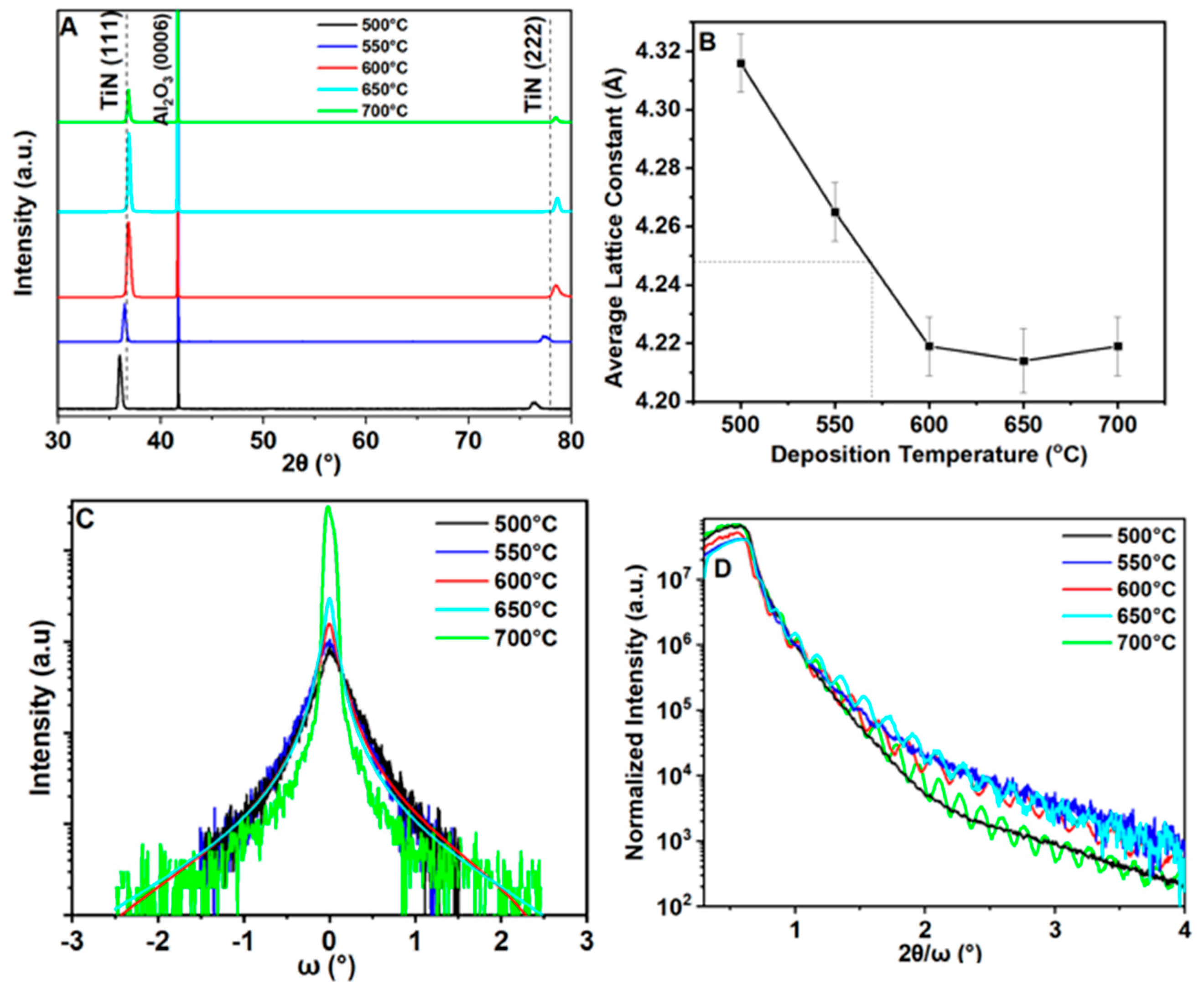
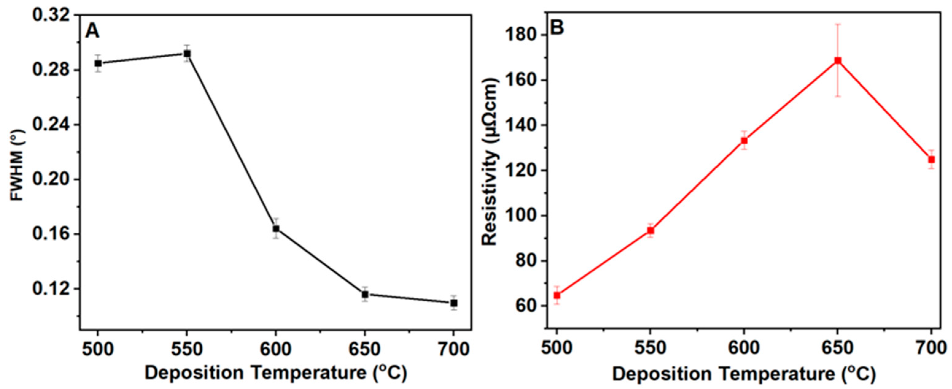
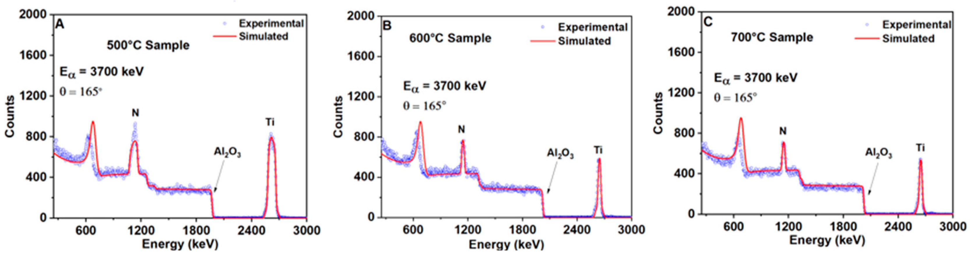
3.1. Texture and Phase Composition

X-ray diffraction (XRD) patterns of the films deposited at different temperatures are shown in Figure 1A. A careful examination of the XRD patterns has been performed using XRD SmartLab studio II software. The patterns of the as-synthesized oxynitride thin films confirmed the formation of single-phase rock-salt TiNO structures with a (111) preferred orientation and its second harmonic peak at (222), indicating a growth of high-quality epitaxial TiNO film. The positions of both (111) and (222) peaks were referenced to the TiN planes presented from the JCPDS data [23]. The results reveal a dependence of the film texture on the substrate temperature. The 2θ angles of the (111) peaks for films grown at 500, 550, 600, 650, and 700 °C were recorded as 35.98, 36.46, 36.84, 36.90, and 36.85, respectively. The slight shifts in the peak position, as shown by the dotted line in Figure 1A, can be due to compositional changes in the film [24], which can significantly impact the film’s properties and performance by altering the crystal structure and lattice parameters. Using the Bragg’s law equation, the d-spacing was calculated, and subsequently, the lattice constants for peaks (111) and (222) of the TiNO films were obtained. The average lattice constant values are plotted as a function of growth temperature in Figure 1B. The theoretical value of the TiN conventional lattice constant, shown by the dotted line in Figure 1B as obtained from literature, is 4.241 Å [25]. The calculated lattice parameters of crystalline TiNO thin films were 4.32, 4.26, 4.22, 4.21, and 4.22 Å for the substrate temperature of 500, 550, 600, 650, and 700 °C, respectively. The lattice parameter decreased significantly with an increase in growth temperature from 500 °C to 600 °C. After that, the difference was minimal between 600 °C and 700 °C. The decrease in the TiNO lattice constants is attributed to the substitution of more N by O, which has smaller ionic radii (1.42 Å) with respect to that of N (1.71 Å) [2]. The partial oxidation of TiN to TiNO leads to gradual transformation from N-rich to O-rich TiNO, which shares the same rock-salt structure, but with a smaller cell parameter. At higher temperatures, the mobility of atoms and molecules increases. This enhanced mobility allows oxygen atoms to diffuse through the film more readily and react with the metal atoms, facilitating the oxidation process, thus more oxygen atoms replace the nitrogen atoms [26].
The Omega rocking curves (ORC) of TiNO film made at 500, 550, 600, 650, and 700 °C are shown in Figure 1C. The full-width at half maxima (FWHMs) were found to be 0.285°, 0.292°, 0.164°, 0.116°, and 0.110°, respectively, and the trend is illustrated in Figure 2A. The values of FWHM reduce as the growth temperature increases, with the film made at 700 °C exhibiting a relatively higher crystallinity compared to the ones made at lower temperatures. The movement of atoms arriving on the substrate depends on the temperature since it determines the activation energy of the growth mechanism of the film on the substrate [25]. Higher substrate temperatures increase the mobility of adatoms (atoms arriving on the substrate) on the surface, allowing them to find more energetically favorable lattice sites and promoting better crystallinity [21]. It is also observed from the XRR curve that the film at a lower temperature is relatively rougher as no Kiessig fringes are observed, as well as lower intensity at higher 2θ/ꞷ angle as shown in Figure 1D. In all the six films, the critical angle ranges from 0.5625° to 0.5775° showing very similar density of between 5 and 5.1 g/cm3 which is close to the theoretical density (5.21 gcm−3) of TiN [27].
Figure 2B, shows the resistivity of the films. The resistivity of thin films is significantly influenced by the growth temperature during deposition, with several variables including phase formation, defect density, strain effects, surface and interface quality, and other elements coming into play [28]. High temperatures may promote oxidation or reaction with residual gases which can lead to the formation of high-resistivity phases or interfacial layers [28]; which explains the rise in resistivity when deposition temperature was raised from 500 °C to 650 °C. It is worth noting that the specific relationship between growth temperature and resistivity can vary significantly depending on the material, deposition method, and other process parameters [29]. The 700 °C sample has a slightly lower resistivity compared to the 650 °C sample, which might be due to its greater crystallinity. The AFM images of the as-deposited thin films are shown in Figure 3. The root mean square (rms) values obtained were 0.59 nm, 0.431 nm, 0.36 nm, 0.352 nm, 0.345 nm for films made at 500, 550, 600, 650, and 700 °C, respectively. This shows that the roughness of the films relatively reduces with increase in the growth substrate temperature but the magnitude reduction is not significant. A minor change in the film roughness with an increase in the substrate temperature may be associated with inter-grain coalescence at higher temperatures.

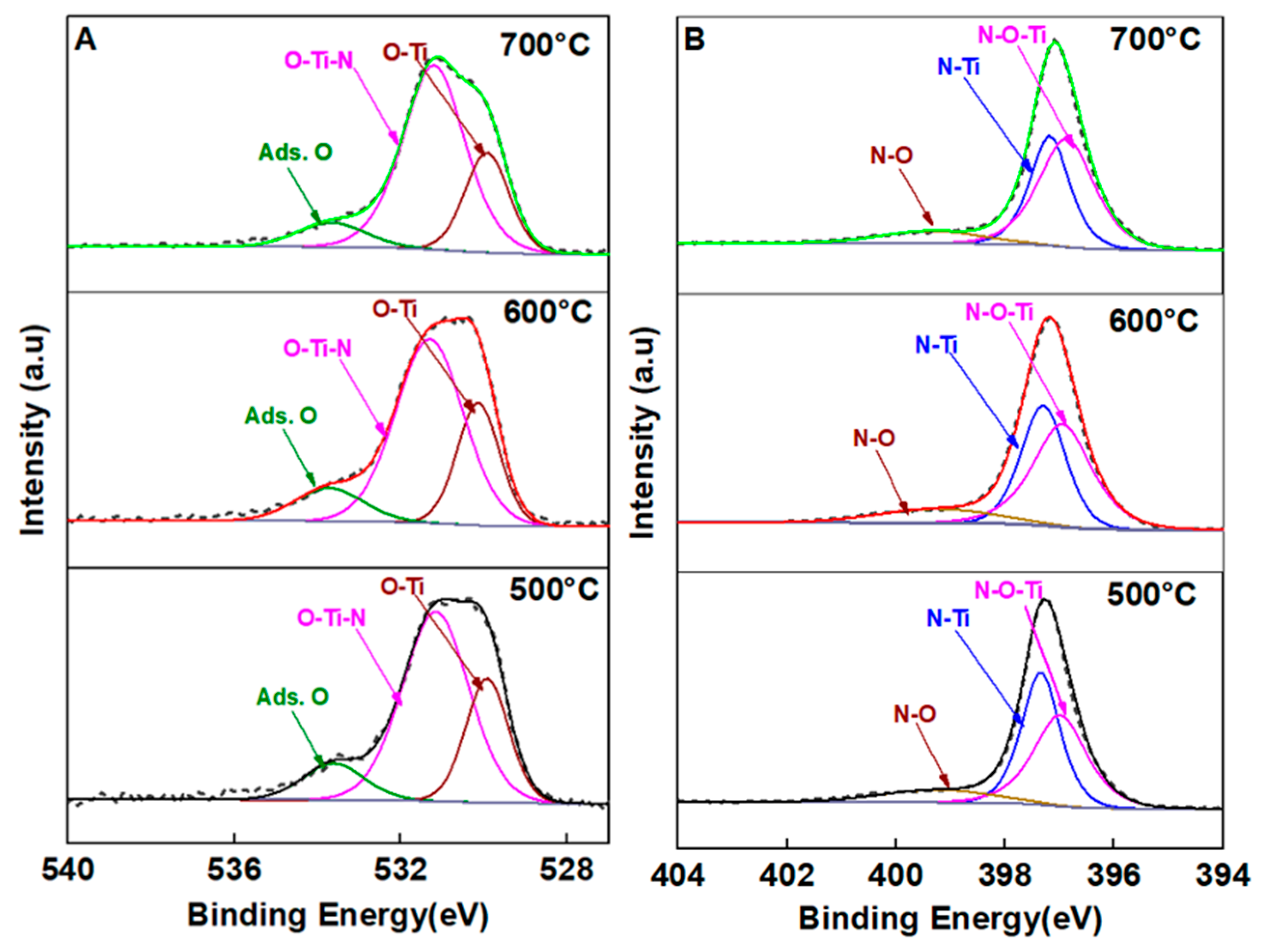
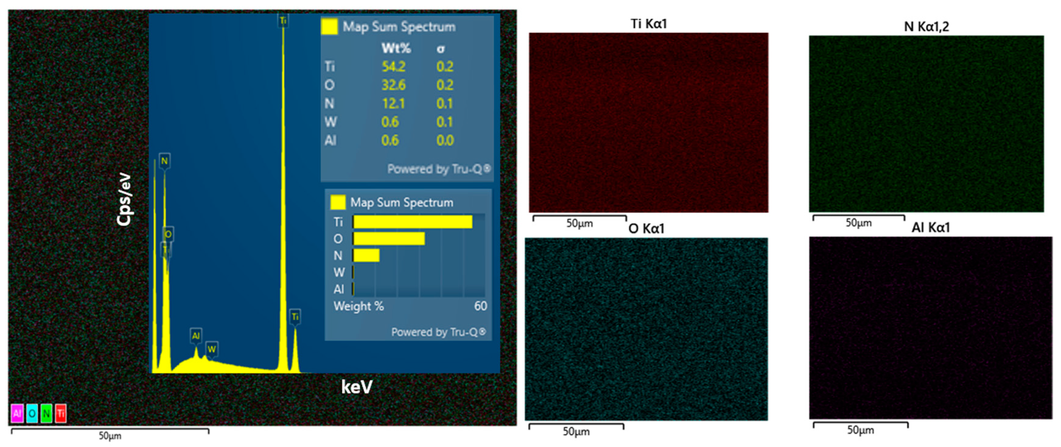
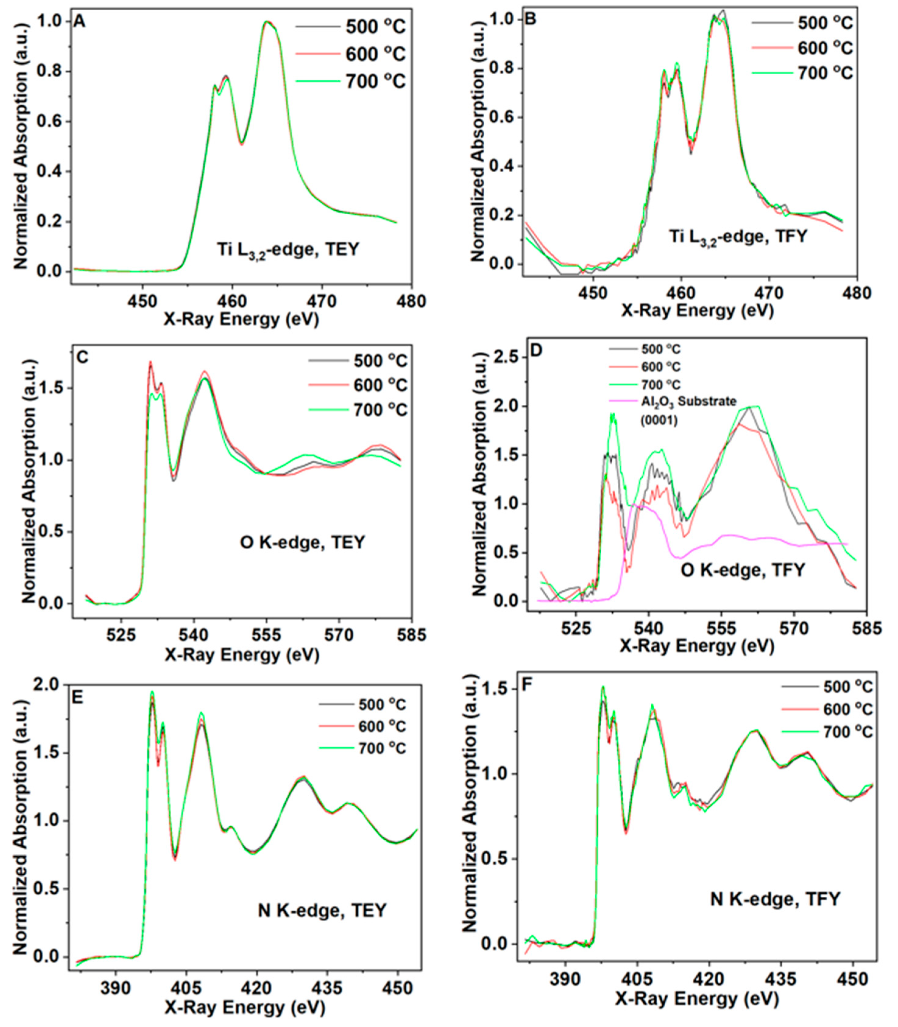
3.2. Chemical Composition

The atomic composition of Ar+ ion sputter-cleaned TiNO thin films obtained from XPS measurements is shown in Table 2 and the survey core level lines originating from Ti (Ti2s, Ti2p, Ti3s, Ti3p), N1s, O1s and C1s, is presented in Figure 4A. The presence of O1s peaks at 530.6–531.4 eV highlighted the presence of oxynitride and oxide species (TiNO, TiO2) in the film. The formation of TiNO takes place via partial oxidation of TiN in the presence of oxygen as the following reaction: T i N 1 2 ( O 2 ) T i N O 1 2 ( O 2 ) T i O 2 + 1 2 N 2 . Depending on the deposition temperature and oxygen pressure, the partially oxidized TiNO phase can be further converted to an anatase or rutile phase TiO2 upon complete oxidation [12]. The oxidation of TiN to TiNO/TiO2 even in vacuum condition is caused by the presence of residual oxygen in the PLD chamber [19]. Even though TiN is chemically stable, oxide layer formation at the surface is still thermodynamically favorable [30]. Analysis of chemical modification in the surface region was carried out by means of a sputter depth profile. The topmost layer was removed by a step-by-step manner and spectra of all major core levels were recorded after each sputtering sequence to reveal the elemental and chemical composition as a function of depth. The representative result of one film is shown in Figure 4B. It is observed that after the first cycle of sputtering, the atomic percentage of C1s drastically reduces by ~92.1%, with a slight reduction in O1s (~11.9%) and an increase in Ti2p (~33.5%) and N1s (~32%). Subsequent sputter cycles show a small variation in the composition indicating that the bulk composition does not change much.
The fitting procedure allowed the evaluation of the signals by determining the peak position, height, and full-width half maxima. High-resolution core-level XPS spectra peaks of Ti2p (Figure 4C), O1s, and N1s were also recorded. The binding energies and their species assignment are listed in Table 3. To represent the entire Ti2p (450–475 eV) spectrum, ten different peaks have been fitted using constraints that are based on the physical principles of these peaks. Fitting Parameters for Ti2p spectra were developed using data from the NIST XPS database [31] and selected literature references [32,33,34,35]. Adventitious carbon, C1s set at 284.8 eV was used as an internal standard for binding energy calibration, and in this case, the quoted binding energies are allowed to vary by ±0.1–0.2 eV following the uncertainty with this method [35]. A detailed representation of the different contributing species of Ti2p peak is shown in Figure 4C. Three peaks are identified, each spin–orbit split into doublets with j values of 1/2 and 3/2. The peak positions at 455.03 eV, 456.2 eV, and 458.51 eV identified as TiN 2p3/2, TiNO 2p3/2, and TiO2 2p3/2 respectively matched well with the literature binding energies values [34,35,36,37,38]. The gap between the 2p-doublet peaks (2p3/2 and 2p1/2) of TiN, TiNO, and TiO2 remained fairly constant with an average of 5.9, 5.86, and 5.7 eV for samples made at 500 °C, 600 °C, and 700 °C. The signal at the lowest BE, at 455.03 eV is a characteristic of nitride species [36]. Although the nitride peak exhibits the highest intensity, it is observed that its area and subsequently the molecular fraction decreases as the growth temperature increases as illustrated in Figure 4D. The signal at 456.2 eV has been related to the intermediate species, in which both N and O are bound to Ti atoms [39]. The formation of the species can be explained by a mechanism where the laser-ejected titanium nitride particulates react with residual oxygen to form Ti-N-O groups [40,41]. TiNO species has a rock-salt structure, which is similar to TiN but with a smaller lattice parameter. It is thought to exist at the boundary between nitride and oxide phase. The JCPDS data for TiNO (called deficient TiN) and pure TiN are very similar, so what is seen in XRD can be a mixture of both. The signal at 458.51 eV has been attributed to oxidized species Ti-O [31]. Its area and the molecular fraction slightly increase as the growth temperature increases. The N1s core-level peak signals shown in Figure 5B with BE at 397.3 ± 0.1 eV is attributed to N-Ti species, and the peak at 396.86 eV has been related to the above-mentioned intermediate species of N-O-Ti. A signal of adsorbed (chemisorbed) N-O is detected at about 399.1 eV. The O1s peaks, shown in Figure 5A, have been assigned the oxide (O-Ti) at 529.97 eV, the oxynitride (O-Ti-N) at 531.20 eV and adsorbed oxygen at 533.65 eV. The O1s at 533.65 is connected to oxygen atoms near defects (vacancies) or other adsorbates. In addition to the three main peaks, two plasmon peaks at 457.93 eV for TiN and 459.1 eV for TiNO, along with their spin–orbit splitting counterparts are visible after the fitting procedure. Plasmon peaks are caused by interactions of the emitted photoelectrons with free electrons [33]. These electrons can be excited into empty states and can be described as collective oscillations [32,42].
The XPS percentage molecular fractions of TiN, TiNO, and TiO2 plotted against the substrate temperature is shown in Figure 4D. It is observed that the fraction of TiN decreased by ~19.1% and the fraction of TiNO increased by 14.5% with an increase in the substrate temperature from 500 °C to 700 °C, while the variation in the molecular fraction of TiO2 was much smaller increasing by ~6.4%. The gas phase formation of TiO2 is due to the higher reactivity of titanium atoms/ions in the laser plume with residual oxygen than with nitrogen atoms [19]. It should be noted that no oxygen or nitrogen was added to the chamber intentionally during any of the film depositions. The TiN thin film is oxidized on the substrate after its formation via a post-deposition time-dependent oxygen diffusion process in the presence of the atmosphere of residual oxygen [19]. As a result, this leads to the formation of Ti-O and Ti-N-O bonding and possibly modification of the chemical (and physical) state of the TiNO and TiN lattice. The accuracy of our fitting procedure is illustrated in Figure 4E, where the atomic ratios (TiNO/TiN) of the areas under the deconvoluted peaks of Ti 2p and N 1s matches extremely well and the area ratio of TiNO/TiN has an increasing trend with an increase in the substrate temperature. The composition of the film was also confirmed by scanning electron microscopy-energy dispersive X-ray spectroscopy (SEM-EDX) measurement as shown in Figure 6, which indicated evenly distributed amounts of Ti, N, and O. Furthermore, the N-RBS spectrum was measured at 3700 keV (nitrogen resonance) for the films. The simulation of the acquired spectrum shown in Figure 7 gave chemical composition values tabulated in Table 4. The simulated and experimental data are comparable with the XPS data.
Along with XPS, X-ray absorption spectroscopy (XAS) measurements were carried out at the N K-edge, O K-edge, and Ti L3,2-edge, which records the excitation of core electrons to unoccupied states. Measurements were performed in electron-yield (TEY) and fluorescent-yield (TFY) modes, which are surface-sensitive (probing depth < ~10 nm) and bulk-sensitive (probing depth > ~100 nm), respectively. The TEY and TFY spectra at the Ti L3,2-edge were nearly identical for the three films, indicating that the average oxidation state of the Ti atoms, both near the surface and in the bulk, are similar for the films deposited at the three temperatures (Figure 8A,B). For the TEY O K-edge spectra, differences are seen with the deposition temperature (Figure 8C), especially the film grown at 700 °C. This suggests a different average coordination environment around the oxygen atoms in the 700 °C film as it is also observed that the rocking curve for the 700 °C film is significantly sharper. The broadness of the peaks is also consistent with the TiO2 phase being amorphous, as observed from the absence of the TiO2 peak in the XRD spectrum, since the spectrum of crystalline TiO2 exhibits sharp peaks around 531 and 533 eV, corresponding to O 2p states hybridized with Ti 3d states and split into t2g and eg levels. The TFY O K-edge spectra had a possible contribution from the sapphire substrate and higher level of noise due to the much weaker signal strength, making it difficult to analyze the spectral shape (Figure 8D). The N K-edge spectra (Figure 8E,F) showed small differences between samples in both the surface and the bulk, which is consistent with the small variation in TiN/TiNO ratio observed by XPS (Figure 4D).

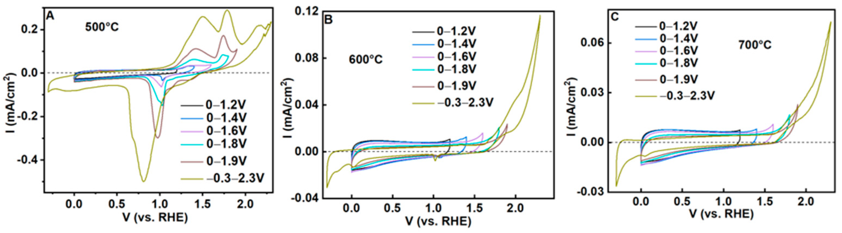
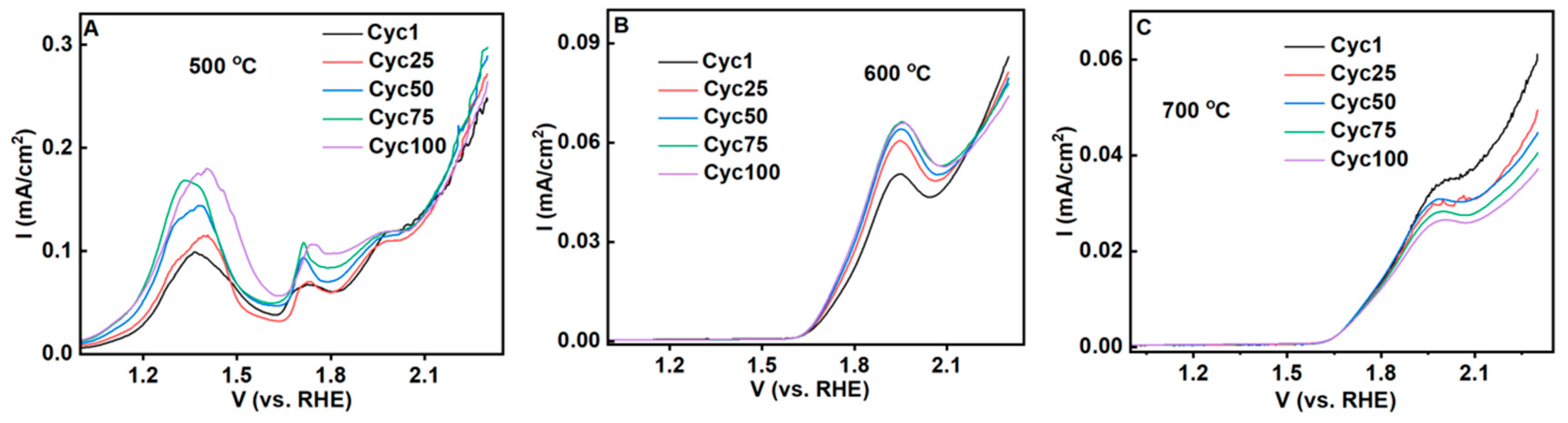
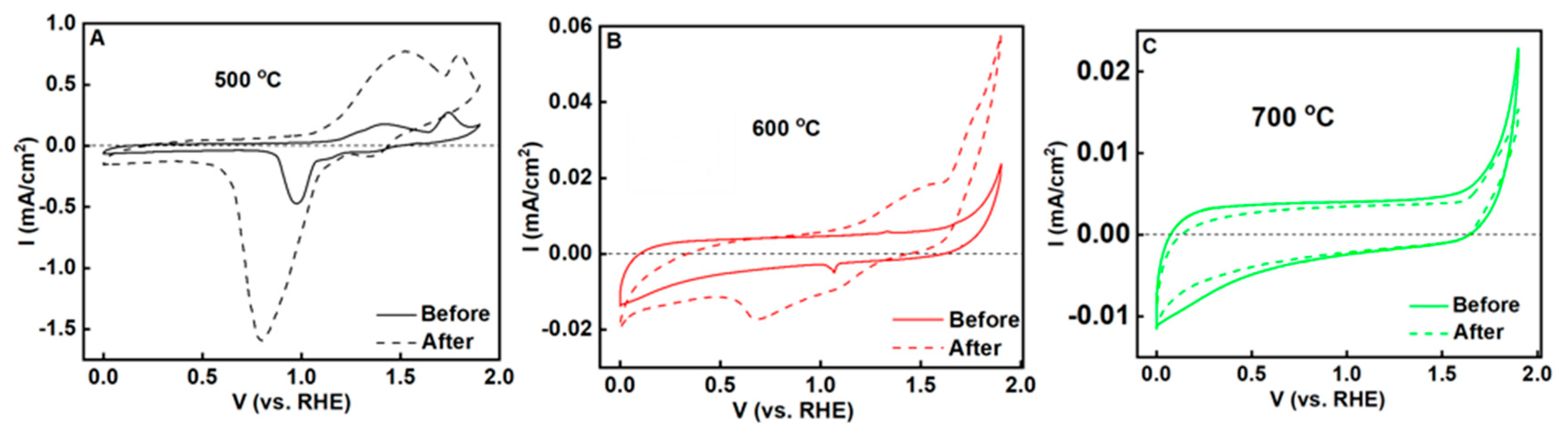
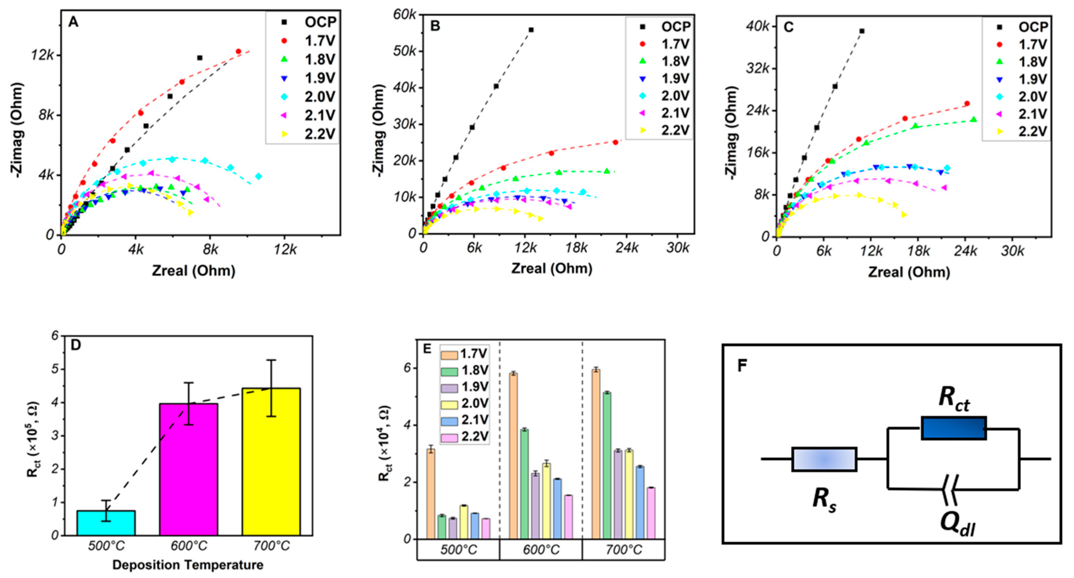
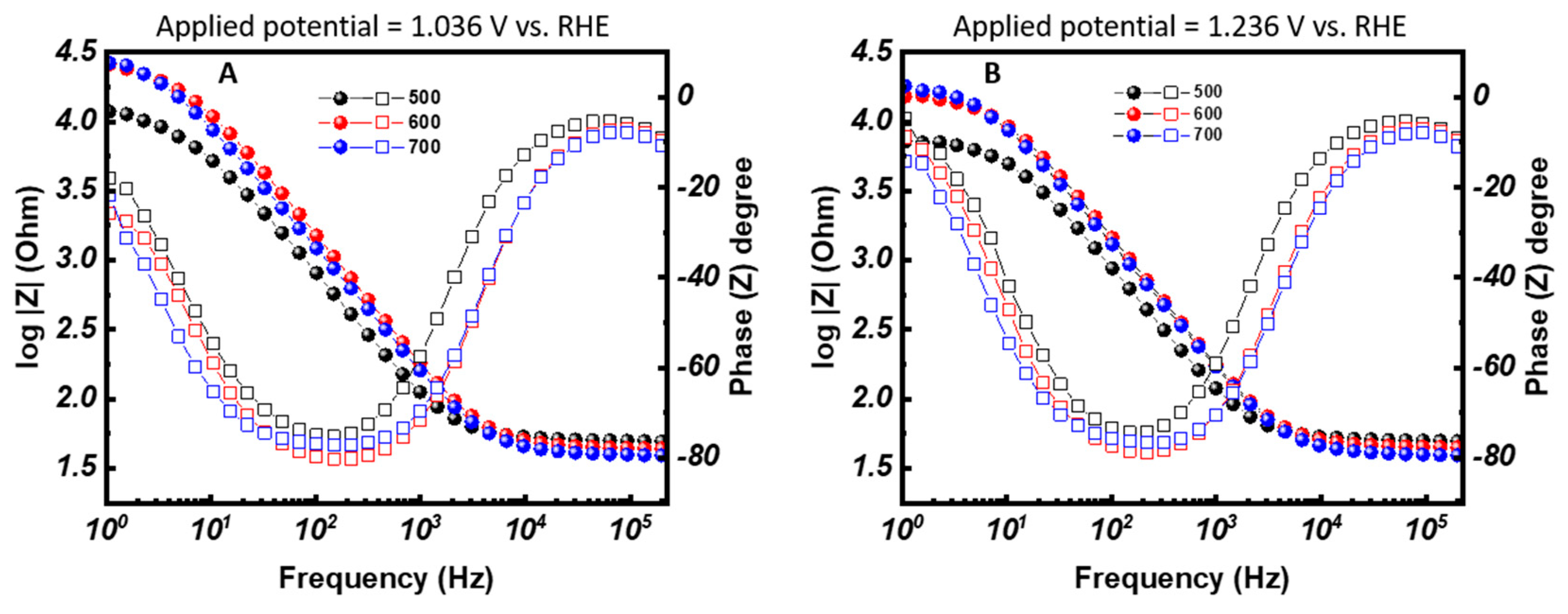
3.3. Electrochemical Properties

The electrochemical activity and stability of the deposited TiNO thin films has also been explored. Their redox behaviors were analyzed by cyclic voltammetry (CV), and the plots are displayed in Figure 9. The potential scan range was increased gradually, and 20 CV cycles were obtained at each scan range for stabilization. The curves displayed in Figure 9 were obtained at the end of each 20-cycle scans. In general, there was no significant change between the 20 CV curves obtained with the same potential scan range. For the 500 °C film, an obvious reduction peak appeared at 1.03 V when the anodic potential scan limit was increased to 1.40 V, and this reduction peak grew in magnitude with the increase in potential range until the anodic potential limit reached 1.60 V. When the scan limit was extended to 1.9 V, a second oxidation peak appeared at 1.72 V. Both the first and second oxidation peaks shifted positive with an increased potential scan range. For the 600 °C TiNO film, the overall current density was smaller than the 500 °C sample. A small reduction peak appeared at 1.08 V when the potential window reached 1.40 V, but in contrast to the 500 °C sample, there was no obvious oxidation peak seen until the potential scan range reached between −0.3 to 2.3 V. The 700 °C sample had the least electrochemical activity, in which no obvious oxidation and reduction peak appeared. For all the films, the current density is observed to be very low compared with state-of-the-art RuO2 and IrO2 catalyst [43], which could indicate low oxygen evolution reaction activity.
In the literature of the electrochemistry of transition metal nitrites/oxides, several arguments exist on the stability and the viability of these material systems as alternative electrode materials. It is widely reported that an oxidized layer is almost always formed on TiN due to the thermodynamically favorable oxidation process in ambient conditions. The oxidation is accelerated in the corrosive operation conditions of the OER [44]. A control of TiN oxidation was made possible through a gas phase oxygenation of the ablated species in residual oxygen gas ambient and regulating the in-diffusion and out-diffusion of oxygen from the oxidized TiN films in a high vacuum condition. The combination of gas phase oxygenation of TiN species and oxygen in(out)-diffusion processes, leads to the formation of more electrochemically stable TiNO film, through the substitutional replacement of the N by O, as has been demonstrated by XPS analysis previously discussed. This TiNO species is an intermediary of the less stable but more electrochemically active TiN and the more stable and less electrochemically active TiO2. A question arises, which is, what happens to the N atoms as it is replaced in the TiN structure/lattice? Does it go on to form interstitial N2 molecules in the oxidized surface layer? [45]. Interstitial N2 molecules would have been visible as a sharp peak around 401 eV in the N K-edge XAS (Figure 8E,F), but we do not observe it. Does the formation of Ti vacancy maintain the charge neutrality due to substitution of N by O [19], and does the interstitial positioning explain the formation of the oxide species? Or does the O species form electrically charged interstitial sites instead of replacing nitrogen? We can hypothesize the explanation of these questions by analyzing the electrochemical activity of the thin films. For instance, the two major oxidation peaks in the 500 °C sample could be due to the higher fraction of the more active TiN and TiNO as seen in the XPS results, leading to the formation of surface Ti-OH* and Ti-O* that could serve as precursors to OER. Most reserchers have reported that the metal site acts as the major active site for OER, which is in line with other metallic OER catalysts, i.e., IrO2, RuO2, and NiO [43]. The reduction peak in the return scan (Figure 9A) shows a partial reduction in the oxidized TiN.
To further investigate the electrochemical performance, the films were also measured by running 100 linear sweep voltammetry (LSV) scans after the CV cycles, as shown in Figure 10. The LSV curve of the 500 °C sample exhibited an unsystematic variation with the cycle number. From 1.0 to 2.3 V, oxidation peaks are observed and the value at the respective voltage (1.36, 1.74, and 2.30 V) tends to increase with cycle number. This could be due to the complex surface oxidation and oxygen evolution processes occurring at the same time. In an early study by Logothetidis et al., O atom can easily enter into the TiN lattice structure by the reaction of oxygen with the weakly bonded TiN under room temperature [46]. In 2010, Avasarala et al. also illustrated that TiN can be easily transformed into titanium oxide under the electrochemical oxidation process with application of potential [44]. Similarly, for the 600 °C TiNO, current density increases with cycle number at 1.95 V; however, after the 75th cycle, the value does not change significantly, which may indicate a saturated formation of Ti oxides. However, current increases with the cycle number at 2.3 V, which could be illustrating an OER dominated reaction. Compared with the 500 °C and 600 °C samples, the LSV performance of 700 °C thin film has the more systematical and smoother variation and this could be due the higher molecular fraction of the TiNO phase, causing a higher surface oxidation resistance (Figure 4C).
To study the stability of the thin films, CV curves were measured before and after the 100 LSV scans, as shown in Figure 11. The 500 °C sample has the most obvious variation on the CV curves, and a relatively small CV change exists on the 600 °C sample. On the contrary, only a slight current diminishment appears on the 700 °C sample, indicating a higher electrochemical stability. As seen in the ORC (Figure 1C), the sample grown at 700 °C has a higher crystallinity. We believe such a good alignment of the crystallites in the (111) orientation contributes to the stability of the 700 °C sample. An increased level of crystallinity in a thin film generally leads to improved electrochemical stability, i.e., the film is less prone to degradation or changes in its electrochemical properties after repeated charge–discharge cycles [47]. Higher crystallinity indicates a lower defect density because the atoms are arranged more regularly in a repeating pattern, while lower crystallinity indicates a higher presence of imperfections like dislocations and vacancies due to a less organized atomic arrangement [48]. More defects could mean additional active sites available for electrocatalytic activity [49].
Nyquist plots obtained from electrochemical impedance spectroscopy (EIS) measurements performed at different voltages are shown in Figure 12A–C [50]. Under the open circle potential (OCP), the semicircle part does not display in the Nyquist plot at the relative lower frequency range because it is difficult for charge transfer to happen at 10 mV perturbation. Far away from potentials where there can be redox reactions (film oxidation or OER), there is no charge transfer element, only double layer capacitance. With the increase in voltage from 1.7 to 2.2 V, semicircle structure becomes more obvious with a decrease in diameter, indicating a reduction in the charge transfer resistance. This is because electrochemical reactions happen more easily under higher voltage, which provide larger energy for breakthrough of the energy barrier. For the 500 °C thin film, the charge transfer variation is not systematic with the voltage, which could be caused by the combination of complex surface oxidation processes and OER, while variation in the 600 °C film is more regular. However, the approximate resistance value obtained at 2.0 V is abnormally larger compared to the one obtained at 1.9 V, which may be caused by the participation of the surface oxidation process. The charge transfer resistance of the 700 °C sample exhibits a smoother change with the increase in voltage.
The values of measured charge transfer resistance under different potential were summarized in Figure 12D,E. Comparing the charge transfer resistance values with a given working potential from 1.7 to 2.2 V, the value of the corresponding sample at open circle potential (OCP) is super high because of the extremely facile charge transfer kinetics, when 10 mV oscillation potential was barely applied. On the other hand, the respective resistance value shows an obvious increase with deposition temperature, coinciding with the variation in electrochemical activity which had been explained by CV and LSV data plots. This illustrates a decrease in the activity due to enrichment of the TiNO phase and a decrease in electrochemical active sites in the TiN lattice structure with the increase in the deposition temperature. Additionally, the higher saturated O level in the TiNO lattice structure for the 700 °C sample hinder further surface oxidation process which may occur around 2.0 V. EIS data were fitted using different fitting models, and after several attempts, it was observed that the Randel’s equivalent model shown in Figure 12F was the most suitable fit for the data. Good matching between scatter points with the corresponding fitted dash lines indicates the appropriate fitting model. The model elaborates the charge transfer characteristics of the as fabricated thin film structures. Rs, Rct, and Qdl represent the solution resistance, charge transfer resistance, and the constant phase element (CPE) related double layer capacitor, respectively. Because of the complex structure between the electrode and the KOH electrolyte interface, rather than a pure capacitor, a CPE was utilized in the equivalent circuit, which connects in parallel with a charge transfer resistor related element (Figure 12F) [51,52].
To investigate the frequency-dependent electrochemical behavior, Bode magnitude and phase angle plots were analyzed for the films grown at 500 °C, 600 °C, and 700 °C under applied potentials of 1.036 V and 1.236 V vs. RHE and presented in Figure 13A,B. With increasing temperature, a significant decrease in impedance was observed, indicating enhanced ionic and/or electronic conductivity. Additionally, the applied potential influenced the overall impedance response, with higher potential (1.236 V vs. RHE) further reducing the impedance, particularly at lower frequencies, suggesting increased charge transfer activity. The phase angle plots exhibited a shift in the relaxation peak toward higher frequencies with both rising temperature and applied potential, reflecting improved charge carrier mobility and faster interfacial polarization processes. These findings highlight the synergistic effects of thermal activation and electrochemical driving force on the material’s conductivity and electrochemical performance.

4. Conclusions

Titanium oxynitride (TiNO) thin films were successfully prepared using pulsed laser deposition onto sapphire substrates at different growth temperatures. XRD and XPS analyses show that the prepared TiNO films exhibited a mixture of Ti–N, Ti–O–N, and Ti-O chemical binding states. It is reported that the nitride component decreases and oxynitride/oxide components increase as the growth substrate temperature is increased. This temperature dependent oxidation of the metal nitride thin film gives rise to an experimentally observed intermediate species (TiNO) with a good balance of electrochemical stability and activity. As confirmed by the AFM, temperature modulated thin film growth can effectively be used to control the surface atom arrangement for effective design of the active sites; as surface diffusion of adatoms is enhanced into equilibrium sites, thus promoting island coalescence and surface smoothness. This work has also demonstrated that the increase in the fraction of TiNO phase due to higher substrate growth temperatures leads to more stability but less intrinsic activity during electrochemical reaction of the thin film.

Author Contributions

Conceptualization: S.C. and D.K.; methodology: S.C., I.C.-O., W.A., S.N., M.L., E.C., V.C., R.S.K., M.M.-D., C.H. and J.M.; formal analysis: S.C., I.C.-O. and S.N.; funding acquisition: D.K.; investigation: S.C., I.C.-O., W.A., M.L., E.C., S.N., C.H., J.Y., V.C. and R.S.K.; resources: D.K., S.A., E.C., J.Y., M.M.-D. and V.C.; data curation: S.C., I.C.-O., W.A., M.L., J.Y., E.C., J.M., V.C. and D.K.; writing—original draft preparation: S.C. and I.C.-O.; writing—review and editing: S.C., I.C.-O., W.A., S.N., M.L., E.C., J.Y., V.C., R.S.K., M.M.-D., C.H., J.M., S.A. and D.K.; validation: S.C., I.C.-O., W.A., S.N., S.A., M.L., E.C., V.C., R.S.K., J.Y., M.M.-D., C.H. and J.M.; supervision: D.K., S.A., E.C. and J.Y.; project administration: D.K. All authors have read and agreed to the published version of the manuscript.

Funding

This work was supported as part of the Center for Electrochemical Dynamics and Reactions on Surfaces (CEDARS), an Energy Frontier Research Center funded by the U.S. Department of Energy, Office of Science, Basic Energy Sciences at the North Carolina A&T State University under award DE-SC0023415. The work also used resources at the ALS of LBNL, supported by the Director Office of Science, Office of Basic Energy Sciences, of the US Department of Energy under Contract No. DE-AC02-05CH11231. Part of the work was performed using the resources from NSF-PREM Collaborative Research and Education in Advanced Materials Center (grant number DMR-2425119) and the Joint School of Nanoscience and Nanotechnology, a member of the National Nanotechnology Coordinated Infrastructure (NNCI), which is supported by the National Science Foundation (Grant ECCS-2025462). VC work was partially supported by project ELI-RO/RDI/2024-015 and National Nucleu Program LAPLAS VII—contract no. 30N/2023.

Data Availability Statement

The raw/processed data required to reproduce these findings cannot be shared at this time due to technical or time limitations.

Conflicts of Interest

The authors declare that they have no known competing financial interests or personal relationships that could have appeared to influence the work reported in this paper.

Abbreviations

The following abbreviations are used in this manuscript:
TiNOTitanium oxynitride
PLDPulsed laser deposition
XRDX-ray diffraction
XRRX-ray reflectometry
XPSX-ray photo electron spectroscopy
XASX-ray absorption spectroscopy
TiTitanium nitride
TiO2Titanium dioxide
CVDChemical vapor deposition
ALDAtomic layer deposition
TEYTotal electron yield
TFYTotal fluorescent yield
CVCyclic voltammetry
LSVLinear sweep voltammetry
EISElectrochemical impedance spectroscopy
OEROxygen evolution reaction
ORCOmega rocking curve
OCPOpen circuit potential

References

  1. Gebauer, C.; Fischer, P.; Wassner, M.; Diemant, T.; Jusys, Z.; Hüsing, N.; Behm, R.J. Performance of titanium oxynitrides in the electrocatalytic oxygen evolution reaction. Nano Energy 2016, 29, 136–148. [Google Scholar] [CrossRef]
  2. Mucha, N.R.; Som, J.; Choi, J.; Shaji, S.; Gupta, R.K.; Meyer, H.M.; Cramer, C.L.; Elliott, A.M.; Kumar, D. High-Performance Titanium Oxynitride Thin Films for Electrocatalytic Water Oxidation. ACS Appl. Energy Mater. 2020, 3, 8366. [Google Scholar] [CrossRef]
  3. Mohamed, S.H.; Zhao, H.; Romanus, H.; El-Hossary, F.M.; El-Kassem, M.A.; Awad, M.A.; Rabia, M.; Lei, Y. Optical, water splitting and wettability of titanium nitride/titanium oxynitride bilayer films for hydrogen generation and solar cells applications. Mater. Sci. Semicond. Process. 2020, 105, 104704. [Google Scholar] [CrossRef]
  4. Janders, M.; Egert, U.; Stelzle, M.; Nisch, W. Novel thin film titanium nitride micro-electrodes with excellent charge transfer capability for cell stimulation and sensing applications. In Proceedings of the 18th Annual International Conference of the IEEE Engineering in Medicine and Biology Society, Amsterdam, The Netherlands, 31 October–3 November 1996. [Google Scholar] [CrossRef]
  5. Chen, T.-T.; Liu, H.-P.; Wei, Y.-J.; Chang, I.-C.; Yang, M.-H.; Lin, Y.-S.; Chan, K.-L.; Chiu, H.-T.; Lee, C. Porous titanium oxynitride sheets as electrochemical electrodes for energy storage. Nanoscale 2014, 6, 5106–5112. [Google Scholar] [CrossRef] [PubMed]
  6. Chris-Okoro, I.; Som, J.; Cherono, S.; Liu, M.; Nalawade, S.S.; Lu, X.; Wise, F.; Aravamudhan, S.; Kumar, D. Effect of Substrate Temperature on the Electrochemical and Supercapacitance Properties of Pulsed Laser-Deposited Titanium Oxynitride Thin Films. J. Electrochem. Energy Convers. Storage 2025, 22, 011010. [Google Scholar] [CrossRef]
  7. Chatenet, M.; Pollet, B.G.; Dekel, D.R.; Dionigi, F.; Deseure, J.; Millet, P.; Braatz, R.D.; Bazant, M.Z.; Eikerling, M.; Staffell, I.; et al. Water electrolysis: From textbook knowledge to the latest scientific strategies and industrial developments. Chem. Soc. Rev. 2022, 51, 4583–4762. [Google Scholar]
  8. Wang, S.; Lu, A.; Zhong, C. Hydrogen production from water electrolysis: Role of catalysts. Nano Converg. 2021, 8, 4. [Google Scholar] [CrossRef]
  9. Guo, H.; Chen, W.; Shan, Y.; Wang, W.; Zhang, Z.; Jia, J. Microstructures and properties of titanium nitride films prepared by pulsed laser deposition at different substrate temperatures. Appl. Surf. Sci. 2015, 357, 473. [Google Scholar] [CrossRef]
  10. Serro, A.P.; Completo, C.; Colaço, R.; Dos Santos, F.; Da Silva, C.L.; Cabral, J.M.S.; Araújo, H.; Pires, E.; Saramago, B.A. Comparative study of titanium nitrides, TiN, TiNbN and TiCN, as coatings for biomedical applications. Surf. Coat. Technol. 2009, 203, 3701–3707. [Google Scholar] [CrossRef]
  11. Faruque, M.K.; Kwadwo, M.; Xu, Z.; Kumar, D. Fabrication, characterization, and mechanism of vertically aligned titanium nitride nanowires. Appl. Surf. Sci. 2012, 260, 36–41. [Google Scholar] [CrossRef]
  12. Mucha, N.R.; Som, J.; Shaji, S.; Fialkova, S.; Apte, P.R.; Balasubramanian, B.; Shield, J.E.; Anderson, M.; Kumar, D. Electrical and optical properties of titanium oxynitride thin films. J. Mater. Sci. 2020, 55, 5123–5134. [Google Scholar] [CrossRef]
  13. LeClair, P.; Berera, G.P.; Moodera, J.S. Titanium nitride thin films obtained by a modified physical vapor deposition process. Thin Solid Films 2000, 376, 9–15. [Google Scholar] [CrossRef]
  14. Ali, S.; Magnusson, R.; Pshyk, O.; Birch, J.; Eklund, P.; Le Febvrier, A. Effect of O/N content on the phase, morphology, and optical properties of titanium oxynitride thin films. J. Mater. Sci. 2023, 58, 10975. [Google Scholar] [CrossRef]
  15. El-Hossary, F.M.; Negm, N.Z.; Abd El-Rahman, A.M.; Raaif, M.; Abd Elmula, A.A. Properties of titanium oxynitride prepared by RF plasma. Adv. Chem. Eng. Sci. 2014, 5, 1. [Google Scholar] [CrossRef]
  16. Acosta, E. Thin Films/Properties and Applications. In Thin Films; Intech Open: London, UK, 2021. [Google Scholar] [CrossRef]
  17. Geremew, T. Thin Film Deposition and Characterization Techniques. J3DPA 2022, 1, 1. [Google Scholar] [CrossRef]
  18. Chrisey, D.B.; Hubler, G.K. Pulsed Laser Deposition of Thin Films; John Wiley & Sons: Hoboken, NJ, USA, 1994. [Google Scholar]
  19. Roy, M.; Sarkar, K.; Som, J.; Pfeifer, M.A.; Craciun, V.; Schall, J.D.; Aravamudhan, S.; Wise, F.W.; Kumar, D. Modulation of Structural, Electronic, and Optical Properties of Titanium Nitride Thin Films by Regulated In Situ Oxidation. ACS Appl. Mater. Interfaces 2023, 15, 4733–4742. [Google Scholar] [CrossRef]
  20. Shepelin, N.A.; Tehrani, Z.P.; Ohannessian, N.; Schneider, C.W.; Pergolesi, D.; Lippert, T. A practical guide to pulsed laser deposition. Chem. Soc. Rev. 2023, 52, 2294. [Google Scholar] [CrossRef]
  21. Zhang, D.; Guan, L.; Li, Z.; Pan, G.; Tan, X.; Li, L. Simulation of island aggregation influenced by substrate temperature, incidence kinetic energy and intensity in pulsed laser deposition. Appl. Surf. Sci. 2006, 253, 874–880. [Google Scholar] [CrossRef]
  22. Bele, M.; Jovanovič, P.; Marinko, Z.; Drev, S.; Šelih, V.S.; Kovač, J.; Gaberšček, M.; Koderman Podboršek, G.; Draẑič, G.; Hodnik, N.; et al. Increasing the oxygen-evolution reaction performance of nanotubular titanium oxynitride-supported Ir nanoparticles by a strong metal–support interaction. ACS Catal. 2020, 10, 13688–13700. [Google Scholar] [CrossRef]
  23. Tian, X.; Luo, J.; Nan, H.; Zou, H.; Chen, R.; Shu, T.; Li, X.; Li, Y.; Song, H.; Liao, S.; et al. Transition Metal Nitride Coated with Atomic Layers of Pt as a Low-Cost, Highly Stable Electrocatalyst for the Oxygen Reduction Reaction. J. Am. Chem. Soc. 2016, 138, 1575. [Google Scholar] [CrossRef]
  24. Harrington, G.F.; Santiso, J. Back-to-Basics tutorial: X-ray diffraction of thin films. J. Electroceram. 2021, 47, 141. [Google Scholar] [CrossRef]
  25. Callister, W.D.; Rethwisch, D.G. Fundamentals of Materials Science and Engineering, 10th ed.; John Wiley & Sons: Hoboken, NJ, USA, 2020. [Google Scholar]
  26. Rasic, D.; Sachan, R.; Chisholm, M.F.; Prater, J.; Narayan, J. Room Temperature Growth of Epitaxial Titanium Nitride Films by Pulsed Laser Deposition. Cryst. Growth Des. 2017, 17, 6634. [Google Scholar] [CrossRef]
  27. Rumble, J. CRC Handbook of Chemistry and Physics, 102nd ed.; CRC Press: Boca Raton, FL, USA, 2017; Chapter: Ionic Conductivity and Diffusion at Infinite Dilution. [Google Scholar]
  28. Goswami, A. Thin Film Fundamentals; New Age International: New Delhi, India, 1996. [Google Scholar]
  29. Sambles, J.R. The resistivity of thin metal films—Some critical remarks. Thin Solid Films 1983, 106, 321–331. [Google Scholar] [CrossRef]
  30. Saha, N.C.; Tompkins, H.G. Titanium nitride oxidation chemistry: An X-ray photoelectron spectroscopy study. J. Appl. Phys. 1992, 72, 3072–3079. [Google Scholar] [CrossRef]
  31. Wagner, C.D.; Naumkin, A.V.; Kraut-Vass, A.; Allison, J.W.; Powell, C.J.; Rumble, J.R., Jr. NIST Standard Reference Database 20; Version 3.4 (Web Version); National Institute of Standards and Technology: Gaithersburg, MD, USA, 2003; Volume 20899. [Google Scholar]
  32. Greczynski, G.; Hultman, L. A step-by-step guide to perform x-ray photoelectron spectroscopy. J. Appl. Phys. 2022, 132, 011101. [Google Scholar] [CrossRef]
  33. Stevie, F.A.; Donley, C.L. Introduction to X-ray photoelectron spectroscopy. J. Vac. Sci. Technol. A 2020, 38, 063204. [Google Scholar] [CrossRef]
  34. Jaeger, D.; Patscheider, J. A complete and self-consistent evaluation of XPS spectra of TiN. J. Electron Spectrosc. Relat. Phenom. 2012, 185, 523–534. [Google Scholar] [CrossRef]
  35. Biesinger, M.C.; Lau, L.W.; Gerson, A.R.; Smart, R.S.C. Resolving surface chemical states in XPS analysis of first row transition metals, oxides and hydroxides: Sc, Ti, V, Cu and Zn. Appl. Surf. Sci. 2010, 257, 887–898. [Google Scholar] [CrossRef]
  36. Chan, M.; Lu, F. X-ray photoelectron spectroscopy analyses of titanium oxynitride films prepared by magnetron sputtering using air/Ar mixtures. Thin Solid Films 2009, 517, 5006–5009. [Google Scholar] [CrossRef]
  37. Odusanya, A.A.; Schall, J.D.; Pfeifer, M.A.; Wright, J.; Martin, C.; Craciun, V.; Kumar, D. Optical properties of unoxidized and oxidized titanium nitride thin films. J. Mater. Sci. Mater. Eng. 2025, 20, 2. [Google Scholar] [CrossRef]
  38. Chris-Okoro, I.; Cherono, S.; Akande, W.; Nalawade, S.; Liu, M.; Martin, C.; Craciun, V.; Kim, R.S.; Mahl, J.; Cuk, T.; et al. Optical and Plasmonic Properties of High-Electron-Density Epitaxial and Oxidative Controlled Titanium Nitride Thin Films. The J. Phys. Chem. C 2025, 129, 3762–3774. [Google Scholar] [CrossRef]
  39. Zukalova, M.; Prochazka, J.; Bastl, Z.; Duchoslav, J.; Rubacek, L.; Havlicek, D.; Kavan, L. Facile conversion of electrospun TiO2 into titanium nitride/oxynitride fibers. Chem. Mater. 2010, 22, 4045–4055. [Google Scholar] [CrossRef]
  40. Radecka, M.; Pamula, E.; Trenczek-Zajac, A.; Zakrzewska, K.; Brudnik, A.; Kusior, E.; Kim-Ngan, N.T.; Balogh, A.G. Chemical composition, crystallographic structure and impedance spectroscopy of titanium oxynitride TiNxOy thin films. Solid State Ion. 2011, 192, 693–698. [Google Scholar] [CrossRef]
  41. Chen, H.; Lu, F. Oxidation behavior of titanium nitride films. J. Vac. Sci. Technol. A 2005, 23, 1006–1009. [Google Scholar] [CrossRef]
  42. Moulder, J.F.; Stickle, W.F.; Sobol, P.E.; Bomben, K.D. Handbook of X-Ray Photoelectron Spectroscopy; Physical Electronics Inc.: Eden Prairie, MN, USA, 1995. [Google Scholar]
  43. McCrory, C.C.; Jung, S.; Peters, J.C.; Jaramillo, T.F. Benchmarking heterogeneous electrocatalysts for the oxygen evolution reaction. J. Am. Chem. Soc. 2013, 135, 16977–16987. [Google Scholar] [CrossRef]
  44. Avasarala, B.; Haldar, P. Electrochemical oxidation behavior of titanium nitride based electrocatalysts under PEM fuel cell conditions. Electrochim. Acta 2010, 55, 9024–9034. [Google Scholar] [CrossRef]
  45. Esaka, F.; Furuya, K.; Shimada, H.; Imamura, M.; Matsubayashi, N.; Sato, H.; Nishijima, A.; Kawana, A.; Ichimura, H.; Kikuchi, T. Comparison of surface oxidation of titanium nitride and chromium nitride films studied by x-ray absorption and photoelectron spectroscopy. J. Vac. Sci. Technol. A Vac. Surf. Film. 1997, 15, 2521–2528. [Google Scholar] [CrossRef]
  46. Logothetidis, S.; Meletis, E.I.; Stergioudis, G.; Adjaottor, A.A. Room temperature oxidation behavior of TiN thin films. Thin Solid Films 1999, 338, 304–313. [Google Scholar] [CrossRef]
  47. Zhang, Y.; Marschilok, A.C.; Takeuchi, K.J.; Kercher, A.K.; Takeuchi, E.S.; Dudney, N.J. Understanding how structure and crystallinity affect performance in solid-state batteries using a glass ceramic LiV3O8 cathode. Chem. Mater. 2019, 31, 6135–6144. [Google Scholar] [CrossRef]
  48. Wang, H.; Fan, W.; Yang, S.; Gong, G.; Chen, S.; Jiao, L.; You, F.; Qi, J. Deeply understanding electrocatalytic oxygen evolution reaction from the perspective of defect structures. Chem. Eng. J. 2024, 499, 156124. [Google Scholar] [CrossRef]
  49. Wang, L.; Peng, C.; Lin, H.; Zhao, B. Unraveling the role of defects in electrocatalysts for water splitting: Recent advances and perspectives. Energy Fuels 2022, 36, 11660–11690. [Google Scholar] [CrossRef]
  50. Lazanas, A.C.; Prodromidis, M.I. Electrochemical impedance spectroscopy—A tutorial. ACS Meas. Sci. Au 2023, 3, 162–193. [Google Scholar] [CrossRef] [PubMed]
  51. Bredar, A.R.; Chown, A.L.; Burton, A.R.; Farnum, B.H. Electrochemical Impedance Spectroscopy of Metal Oxide Electrodes for Energy Applications. ACS Appl. Energy Mater. 2020, 3, 66. [Google Scholar] [CrossRef]
  52. Balaguera, E.H.; Allagui, A. Limit capacitance of the constant phase element. J. Energy Storage 2024, 90, 111801. [Google Scholar] [CrossRef]
Figure 1. (A) X-ray diffraction patterns for TiNO films grown at different substrate temperatures, (B) average lattice parameter versus deposition temperature, (C) rocking curves, and (D) X-ray reflectivity curves of TiNO films versus the deposition temperature.
Metals 15 00497 g001
Figure 2. (A) Full width at half maximum (FWHM) of (111) peaks as a function of temperature and (B) film resistivity as a function of temperature for films grown at different substrate temperature.
Metals 15 00497 g002
Figure 3. Atomic force microscopy images of TiNO thin films grown at different substrate temperatures of (A) 500 °C, (B) 600 °C, and (C) 700 °C.
Metals 15 00497 g003
Figure 4. (A) X-ray photoelectron spectroscopy survey scan spectra for TiNO thin films grown at different substrate temperatures showing Ti (2s, 2p, 3s, 3p), O1s, and N1s peaks (no background subtraction performed), (B) X-ray photoelectron spectroscopy depth profile of a TiNO film grown at 700 °C, (C) deconvolution of the high-resolution Ti2p spectra for thin films prepared at different substrate temperatures after Ar+ sputtering (including a Shirley background), (D) percentage molecular fractions of TiN, TiNO, and TiO2 present in the thin film samples as a function of substrate temperature, and (E) area ratio of TiNO/TiN obtained from XPS fitting (Ti2p, N1s Spectra) films grown at 500 °C, 600 °C, and 700 °C.
Metals 15 00497 g004
Figure 5. X-ray Photoelectron Spectroscopy (XPS) of (A) O1s and (B) N1s high resolution deconvoluted plots for films grown at 500 °C, 600 °C, and 700 °C.
Metals 15 00497 g005
Figure 6. Scanning electron microscopy–energy dispersive X-ray spectroscopy (SEM-EDX) spectrum showing elemental distribution of a film deposited at 700 °C.
Metals 15 00497 g006
Figure 7. Non-Rutherford backscattering spectrometry (N-RBS). spectra of a TiNO film deposited at (A) 500 °C, (B) 600 °C and (C) 700 °C.
Metals 15 00497 g007
Figure 8. Soft X-ray absorption spectra of TiNO films grown at different substrate temperatures at the (A) Ti L3,2-edge TEY, (B) Ti L3,2-edge TFY (C) O K-edge TEY, (D) O K-edge TFY, and (E) N K-edge TEY and (F) N K-edge TFY.
Metals 15 00497 g008
Figure 9. Cyclic voltammetry plots performed at 100 mV/s for TiNO films grown at different substrate temperatures of (A) 500 °C, (B) 600 °C, and (C) 700 °C.
Metals 15 00497 g009
Figure 10. Linear sweep voltammetry scans performed at 100 mV/s for TiNO films grown at different substrate temperatures of (A) 500 °C, (B) 600 °C, and (C) 700 °C.
Metals 15 00497 g010
Figure 11. Cyclic voltammetry plots performed at 100 mV/s for TiNO films grown at different substrate temperatures of (A) 500 °C, (B) 600 °C, and (C) 700 °C under the potential range between 0 and 1.9 V before and after 100 cycles linear sweep voltammetry scan.
Metals 15 00497 g011
Figure 12. Nyquist plots of TiNO films grown at different substrate temperatures with fitted dash line of (A) 500 °C, (B) 600 °C, (C) 700 °C, and (D) summary of the fitted Rct value under OCP, (E) summary of the fitted Rct value under different applied working potentials, and (F) equivalent circuit of Nyquist plots and data fitting.
Metals 15 00497 g012
Figure 13. Bode magnitude and phase angle plots for the films grown at 500 °C, 600 °C, and 700 °C at the applied potential of (A) 1.036 V vs. RHE, and (B) 1.236 V vs. RHE.
Metals 15 00497 g013
Table 1. Sheet resistance, film thickness, and resistivity values for TiNO thin films deposited at different deposition temperatures.
SampleTemperature
(°C)
Sheet Resistance
(Ω)
Film Thickness
(nm)
Resistivity
(µΩcm)
15006.04107.3 ± 2.064.78 ± 4
255019.0949.0 ± 1.793.54 ± 3
360027.2948.9 ± 2.0133.45 ± 4
465041.9840.2 ± 7.5168.76 ± 16
570025.6048.8 ± 2.0125.05 ± 4
Table 2. Atomic composition obtained from XPS measurement.
Temperature
(°C)
N1s
(%)
Ti2p
(%)
O1s
(%)
50043.2743.7412.99
60041.6944.5113.80
70035.0444.8420.12
Table 3. Spectral fitting parameters of Ti2p, N1s, and O1s: binding energy, FWHM obtained after fitting.
AssignmentBinding Energy (eV)FWHM (eV)
Ti-N 2p 3/2455.051.20
Ti-N 2p ½460.951.44
Ti-N-O 2p 3/2456.122.3 ± 0.02
Ti-N-O 2p 1/2462.102.40
Ti-O2 2p 3/2458.512.4
Ti-O2 2p ½464.212.4
Plasmon Ti-N 2p 3/2457.951.36
Plasmon Ti-N 2p 1/2463.751.36
Plasmon Ti-N-O 2p 3/2459.03 ± 0.062.4
Plasmon Ti-N-O 2p 1/2464.48 ± 0.062.4
N 1s (N-Ti)397.31 ± 0.11.1
N 1s (N-O-Ti)396.861.0
N 1s (N-O)399.102.3
O1s (O-Ti)529.971.27 ± 0.03
O1s(O-Ti-N)531.21.9 ± 0.07
O1s (Ads O)533.651.9 ± 0.01
Table 4. Chemical composition obtained from N-RBS measurement at Nitrogen resonance (* indicates the substrate layer).
Sample NameCharacterization
LayersThickness
(×1015 at./cm2)
CompositionChemical Formula from Composition
700 °C film1500NTiOTiN0.64O0.74
0.270.420.31
2 *100,000AlOAl0.4O0.6
0.40.6
600 °C film1470NTiOTiN0.71O0.38
0.340.480.18
2 *100,000AlOAl0.4O0.6
0.40.6
500 °C film11170NTiOTiN0.62O0.31
0.320.520.16
2 *100,000AlOAl0.4O0.6
0.40.6
Disclaimer/Publisher’s Note: The statements, opinions and data contained in all publications are solely those of the individual author(s) and contributor(s) and not of MDPI and/or the editor(s). MDPI and/or the editor(s) disclaim responsibility for any injury to people or property resulting from any ideas, methods, instructions or products referred to in the content.

