Article

Direct Energy Deposition of Inconel 718 onto Cu Substrate for Bimetallic Structures with Excellent Comprehensive Properties

1
Department of Applied Science and Technology, Politecnico di Torino, Corso Duca Degli Abruzzi 24, 10129 Torino, Italy
2
Consorzio Interuniversitario Nazionale per la Scienza e Tecnologia dei Materiali (INSTM), Via G. Giusti 9, 50121 Firenze, Italy
3
Materials Engineering of Additive Manufacturing, TUM School of Engineering and Design, Technical University of Munich (TUM), Freisinger Landstraße 52, 85748 Garching, Germany
4
Munich Institute of Integrated Materials, Energy and Process Engineering (MEP), Technical University of Munich (TUM), Lichtenbergstraße 4a, 85748 Garching bei München, Germany
5
Chemistry for Technologies Laboratory, Department of Mechanical and Industrial Engineering, University of Brescia, Via Branze 38, 25123 Brescia, Italy
*
Author to whom correspondence should be addressed.
Metals 2025, 15(12), 1292; https://doi.org/10.3390/met15121292
Submission received: 8 October 2025 / Revised: 19 November 2025 / Accepted: 22 November 2025 / Published: 25 November 2025
(This article belongs to the Section Additive Manufacturing)

Abstract

In the aerospace sector, integrating advanced materials with high mechanical capabilities represents the forefront of material science, especially in the field of rocketry. Bimetallic structures are increasingly used in aerospace applications due to their combination of high strength-to-weight ratio, thermal conductivity, and corrosion resistance. Among these, Inconel-copper (In718-Cu) systems are particularly promising, although large differences in thermophysical and mechanical properties between the two materials can induce residual stresses, cracks, and other interfacial defects, requiring careful process control. This study evaluates the fabrication of In718-Cu structures through Direct Energy Deposition (DED), in which In718 was deposited onto a copper substrate using an innovative deposition strategy. Interface quality and microstructure were characterized by SEM/EDS and X-ray diffraction, whereas the mechanical properties were evaluated by nanoindentation, indentation creep, and tensile testing. The results showed that crack-free samples can be achieved, with strong diffusion bonding at the interface and efficient precipitation strengthening on the copper side already in the as-built condition. A uniform distribution of precipitates and consistent penetration depth were also observed, confirming the effectiveness of the deposition strategy for producing reliable In718-Cu components.

1. Introduction

In liquid bi-propellant rocket engines, the thrust chamber operates under extremely severe conditions due to the acceleration of high-temperature combustion gases, which makes thermal management one of the primary design challenges, particularly when the goal is to maximize specific impulse. In the combustion chamber, which is the upstream section of the thrust chamber, the gas temperature can reach values as high as 3200 °C, since higher specific impulse is directly linked to higher chamber temperatures [1]. These extreme thermal and pressure loads demand effective cooling strategies to maintain chamber wall temperatures within limits that ensure structural integrity under thermal stresses, pressure forces, and dynamic loads such as vibrations and thrust. A common solution is to circulate one of the propellants through an intricated network of cooling passages embedded in the thrust chamber walls, with the fuel typically chosen instead of the oxidizer to reduce the risk of material degradation caused by oxidation. This approach is termed regenerative cooling because the coolant is subsequently injected into the combustion process rather than discarded [2].
In conventionally manufactured chambers, the cooling channels are machined into a solid forged component, a process that inherently limits them to straight or moderately simple geometries, after which an outer jacket, often made of a different alloy, is attached. Additive manufacturing (AM), instead, enables the chamber, including intricate, curved, or otherwise optimized internal channels, to be fabricated in a single integrated stage, thereby eliminating the need for separate assembly steps and allowing greater design flexibility.
Regarding the materials, for the manufacturing of thrust chamber components, two main families of metallic materials, namely structural copper alloys and nickel-based superalloys, are generally used. Structural copper alloys are frequently designed with precipitation strengthening mechanisms that provide thermal stability [3]. In these alloys, the limited solubility of the alloying elements in the matrix leads to the formation of stable intermetallic precipitates, which combine very high thermal conductivity with favorable mechanical and chemical properties. This results in an attractive compromise of high-temperature strength, low thermal expansion, and improved resistance to oxidation, making copper-based alloys particularly suitable for applications in high heat flux regions at operating temperatures up to about 700 °C [3,4]. In contrast, nickel-based superalloys are well established as high-temperature corrosion-resistant materials with broad use in aerospace propulsion systems. Their widespread adoption in gas turbines and rocket engines stems from their exceptional tensile strength, creep and fatigue resistance, rupture strength, and oxidation resistance at temperatures approaching 1000 °C [5]. Nevertheless, their relatively low thermal conductivity limits their effectiveness as conductive liners. The performance of monolithic structures, in turn, is largely governed by material selection, and it is often constrained by the intrinsic trade-off between thermal and mechanical properties. A promising approach to overcome these limitations involves the development of multi-material structures, which enable different regions of a component to fulfill distinct functions, thereby surpassing the capabilities of single-material designs. AM has made this approach particularly feasible [6], with successful demonstrations involving various combinations of metals, including stainless steels and Inconel-based composites [7,8,9], which have shown overall enhancements in mechanical and thermal performance, highlighting AM as a key enabler of innovative engineering solutions. The strong interest in these technologies is demonstrated by the fact that in 2020, NASA launched a follow-up project called Rapid Analysis and Manufacturing Propulsion Technology (RAMPT) [10] to further expand large-scale multi-alloy thrust chambers. The main aim of the project was to advance blown powder Directed Energy Deposition (DED) to fabricate integral-channel large-scale nozzles and develop bimetallic and multi-metallic additively manufactured radial and axial joints to optimize material performance. As a result of this project, NASA is currently producing multi-metal components where Cu-based alloy is used for the internal cooling structure, providing the necessary thermal properties, while a Ni-based super alloy, deposited as an external structural jacket, offers high-temperature strength and prevents oxidation [11,12].
The most considered alloys for multi-material trust chambers are GrCop-42, GrCop-84, and Inconel 625 [10,13]. The Cu-Ni binary phase diagram indicates complete solubility without the formation of intermetallic [14], which supports their metallurgical compatibility. Nevertheless, the significant mismatch in properties can induce residual stresses, often causing cracking or delamination at the interface, especially using additive manufacturing processes [15,16]. Therefore, techniques to ensure strong bonding while minimizing such defects are essential. When Inconel alloys are joined with copper-based alloys through AM techniques such as DED, interfacial Marangoni-driven flow promotes mixing of the two materials, resulting in the formation of a new composition at the interface. This mixing, however, can trigger interfacial cracking through mechanisms such as the precipitation of brittle phases or solidification-induced cracking [17]. Previous studies by Gradl et al. [10,11], Preis et al. [18], Iams et al. [19], and Anderson et al. [20] demonstrated that Inconel-GRCop joints produced via additive manufacturing were free from cracking. Conversely, work by Gradl et al. [13] and Hales et al. [21] documented crack formation along the GRCop-Inconel boundary, which raises concerns regarding the structural reliability and load-bearing performance of the joints. These investigations are focused on In625, whose widespread adoption in the aerospace sector stems from its exceptional corrosion resistance and high-temperature mechanical stability that, however, comes at the expense of its extremely high cost. In this context, In718, whose strengthening mechanisms and microstructural evolution differ substantially from those of In625, emerges as a promising candidate for bimetallic structures produced via DED. Additive manufacturing, in fact, can further enhance the intrinsic properties of In718, offering improved ductility and creep resistance compared with In625 [22], thereby extending the potential for more economically viable production routes. To date, only Onuike et al. [23] have provided a preliminary overview of the metallurgical compatibility of In718-GrCop84 joints, in research where the deposited material was the copper alloy, without delivering an in-depth microstructural analysis, thus leaving a significant gap in the literature.
Therefore, the purpose of this study was to systematically investigate the interfacial microstructure and mechanical behavior of DED-fabricated In718–Cu bimetallic structures, and to elucidate the fundamental metallurgical mechanisms governing their bonding and performance. To address this, advanced microstructural characterization and extensive nanoscale mechanical testing were employed to establish the relationships between interfacial features, phase transformations, and mechanical response, providing critical insights into structure–property correlations.
To further clarify the fundamental metallurgical mechanisms, a simplified model system of pure Cu joined with DED-In718 was explored, enabling a more direct evaluation of precipitation behavior and interfacial transformations under the most critical processing conditions. Collectively, these findings advance the understanding of additively manufactured bimetals and contribute to the design of optimized, high-performance multi-material components.

2. Materials and Methods

Pre-alloyed, gas atomized In718 powder (particle size range 45–106 μm), supplied by Mimete (Mimete s.r.l., Biassono, Italy), served as the feedstock for all specimens; the powder’s certified chemical composition conforms to ASTM and is listed in Table 1.
Build trials were performed on a Prima Additive Laserdyne 795 (Prima Additive S.p.A., Pianezza, Italy) consisting of a 5-axis motion system equipped with the REAL_DEDâ coaxial deposition head (Figure 1) and an IPG YLS-3000 Ytterbium-doped fiber laser (IPG Photonics, Marlborough, MA, USA) with a maximum power of 3 kW with a Gaussian distribution in the central wavelength of 1070 nm. A working distance of 7 mm was used, corresponding to the point where the lasers converge, forming a single spot with a diameter (d) of 2 mm.
The process development was carried out in two steps. First, the optimal processing window for the Ni-superalloy was defined using a steel substrate. Next, the joining procedure was developed using a substrate made of extruded pure copper bars whose optical behavior was first evaluated with a Cary 500S UV–Vis–NIR spectrophotometer (Agilent Technologies, Santa Clara, CA, USA) equipped with an integrating sphere in reflectivity mode.
For the first experimental step, cubic-shaped samples having an edge length of 25 mm were built, whose quality was evaluated by means of densification assessment determined by buoyancy according to ASTM B311 [24], and by imaging on representative cross-sections along the build direction after metallographic preparation following standard procedures. All the micrographs were acquired with an optical microscope (OM) LEICA DMI 5000 M (Leica Microsystems GmbH, Wetzlar, Germany). Data extraction was carried out using statistical methods, selecting 30 images from different regions of the examined section. ImageJ 1.54g software was used to evaluate the porosity distribution within each sample. Once the process was established, the metallurgical transformations occurring in the joint were analyzed with various techniques.
Chemical etching was performed with two etchant solutions: a mixture of 1.5 g FeCl3 and 10 mL HCl for the Cu side, and Kalling’s No. 2 for the In718 side. Microstructural morphology was then investigated at multiple magnifications using a TESCAN S9000G field emission scanning electron microscope (FESEM), (TESCAN Group, a.s., Brno, Czech Republic), that was equipped with electron backscatter diffraction (EBSD), and a Thermo-Fisher Phenom XL G2 benchtop SEM (Thermo Fisher Scientific, Waltham, MA, USA) with an energy-dispersive X-ray spectroscopy (EDS) option. EBSD analysis was conducted at 20 keV, 10 nA, with a step size of 0.55 μm.
Phase transformations at the interface were investigated by X-ray micro-diffraction using a Bruker D8 Advance (Bruker Co., Billerica, MA, USA) micro diffractometer with Cu Kα radiation, operated at 40 kV and 40 mA. Diffraction patterns were collected with a step size of 0.01° over a 2θ range of 30–100°. Phase identification was carried out with Bruker DIFFRAC.EVA V6 software. To ensure representative results, multiple regions were examined within a spot window of 500 μm2.
Joint quality was evaluated through mechanical testing at different scales to assess the effect of newly formed intermetallic compounds on the mechanical stability of the alloy.
First, Vickers microhardness was performed with a Leica VMHT apparatus (Leica Microsystems GmbH, Wetzlar, Germany) with a 100 gf load applied for 15 s, following the guidelines outlined in ASTM E384 [25] on both materials, starting from the immediate proximity of the joint to evaluate the joining effect on the global mechanical properties. Then, nanoindentation measurements were performed according to ISO 14557 [26] directly on interfacial regions where liquid-state reactions occurred. The nanohardness, elastic modulus, and indentation creep of the interface were conducted at ambient temperature with a Bruker TI 950 (Bruker Nano Surfaces, Minneapolis, MN, USA) fitted with a Berkovich diamond tip and operated in the load control mode. For the hardness and elastic modulus evaluation, each indentation was applied with a maximum load of 1 mN, with a loading and unloading rate of 200 µN/s, held for 5 s at peak load. A total of 256 indents were performed in a 16 × 16 grid pattern with 5 µm spacing to prevent overlapping plastic zones.
Resulting load–displacement curves were processed with dedicated software to extract nanohardness values, enabling reproducible characterization of the localized mechanical response in the reaction zone and heat-affected areas. Moreover, for indentation creep testing, a load of 8 mN was applied with a loading ramp of 800 µN/s. The load was then held constant for 200 s to monitor the evolution of creep depth over time, followed by unloading at the same rate. The Oliver–Pharr method [27] was employed to determine nanohardness and the elastic modulus, expressed as:
H   = P m a x A c
where Pₘₐₓ is the maximum load and Ac is the projected contact area, calculated as:
A c   =   25.4 · h c 2
For a Berkovich indenter, the contact depth (hc) can be evaluated using:
h c   =   h m a x   ( 0.75 · P / S )
Here, hₘₐₓ is the maximum penetration depth, P is the applied load, and S is the stiffness, defined as the slope of the unloading curve [28]:
S   =   d P / d h
The unloading curve can be described by the power law relationship:
P   =   B · ( h h f ) m
where B and m are fitting constants, and hf is the final unloading depth. Based on elastic contact mechanics, the reduced elastic modulus (Er) is obtained from:
E r   =   1 π · S β · A c
with β being a correction factor that depends on indenter geometry (β = 1.034 for a Berkovich indenter).
Feng and Ngan [29] modeled the creep depth as a function of time (t), expressed as:
h ( t )   =   h i   +   a · t     t i 1 / 2   +   b · t     t i 1 / 4   +   c · t     t i 1 / 8
where hᵢ and tᵢ represent the initial depth and time, and a, b, and c are the best-fitting parameters.
According to Mayo and Nix [30], the creep strain rate ( ε ̇ ) can be determined from:
ε ˙ = 1 h · d h d t
where d h d t is the time derivative of the creep depth obtained from Equation (7). The creep strain rate was used to estimate the stress exponent (n) for different bonding zones by applying the constitutive relation:
ε ̇   =   K · σ n
where K is a material constant and σ is the applied stress.
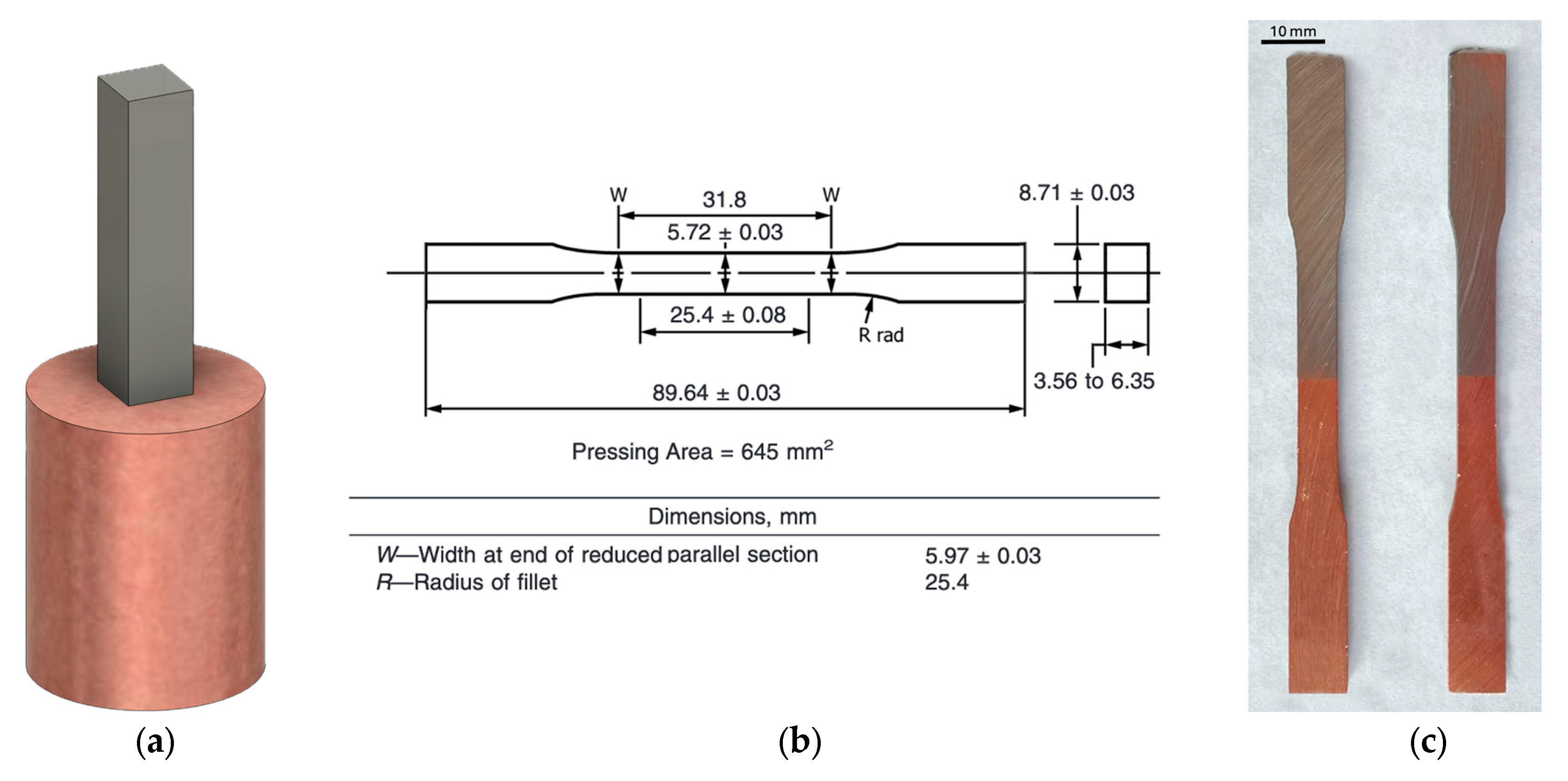
Finally, the overall mechanical performance of the system was tested on tensile specimens prepared according to ASTM E8M [31] (geometry shown in Figure 2) and were tested at room temperature using a Zwick–Roell Z050 (Zwick-Roell GmbH & Co., KG, Baden-Württemberg, Germany) servo hydraulic testing machine, equipped with a 50 kN load cell, at 10−3 s−1. These specimens were machined from a bulk deposition with a parallelepiped shape measuring 12 × 12 × 600 mm3 on a substrate of equal thickness. The objective of this test campaign was to assess the consistency of fracture behavior across the specimens, identify the preferential failure location, and gain insight into the strengthening mechanisms operating at the joint region.

3. Results and Discussion

3.1. DED Processing of In718 on Copper

The optimization of the DED parameters for depositing In718 was carried out using a design-of-experiments approach, with the powder feed rate (f) fixed at 8 g/min based on prior experience on the system. The optimization focused on four variables as follows: laser power (P), scan speed (v), layer-to-layer z-increment (Δz), and the overlap percentage between adjacent tracks (Ov.).
The selection of the initial parameter ranges was based on a literature review on DED processing of In718, with particular attention given to the energy density (ED) [32,33], calculated as:
E D = P v × d × O v × Δ z
Based on this review, the initial experimental window was defined according to the energy density range commonly reported for stable deposition of In718, typically between 125 and 170 J/mm3.
After optimization, the parameter set yielding defect-free In718 depositions was identified, as reported in Table 2.
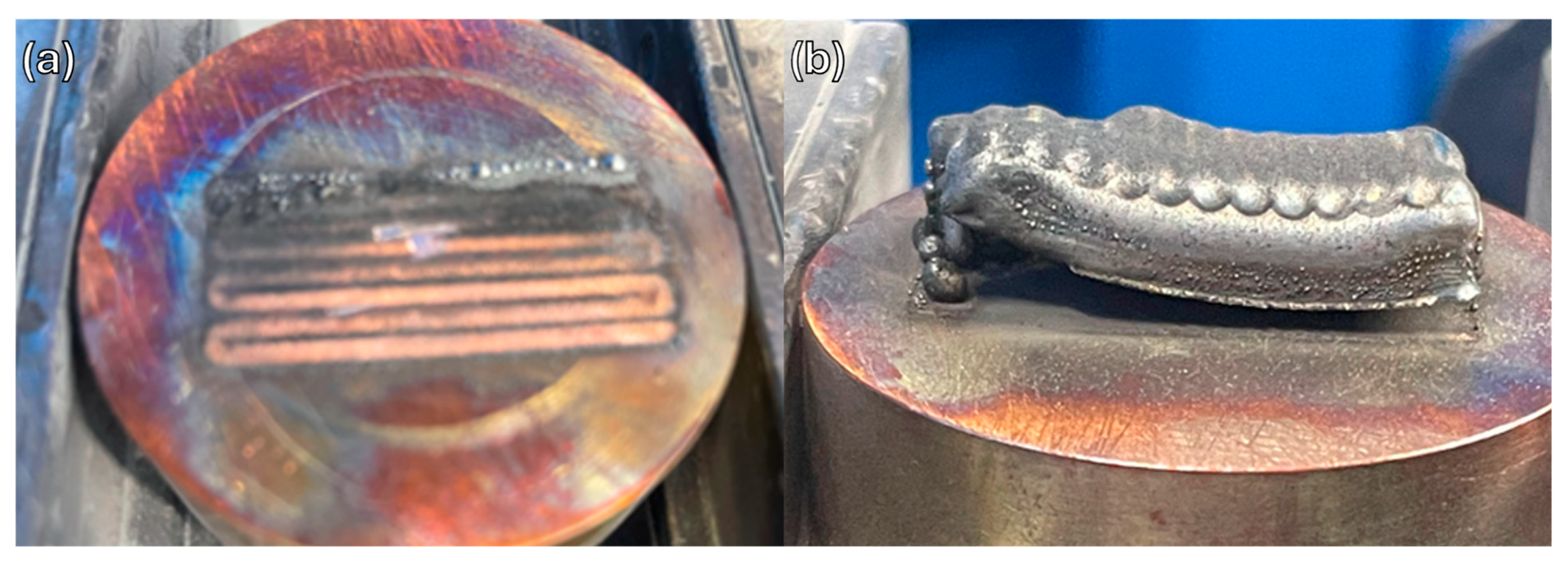
Upon changing the substrate, the initial fabrication trials of the bimetallic structure demonstrated markedly limited diffusion of In718 into Cu, as evidenced in Figure 3. The occurrence of metal agglomeration and balling phenomena, depicted in Figure 3a, resulted in poor surface quality, which hindered the deposition of subsequent layers. Therefore, bonding between layers was inadequate, with metallurgical adhesion occurring only in localized regions, as shown in Figure 3b.
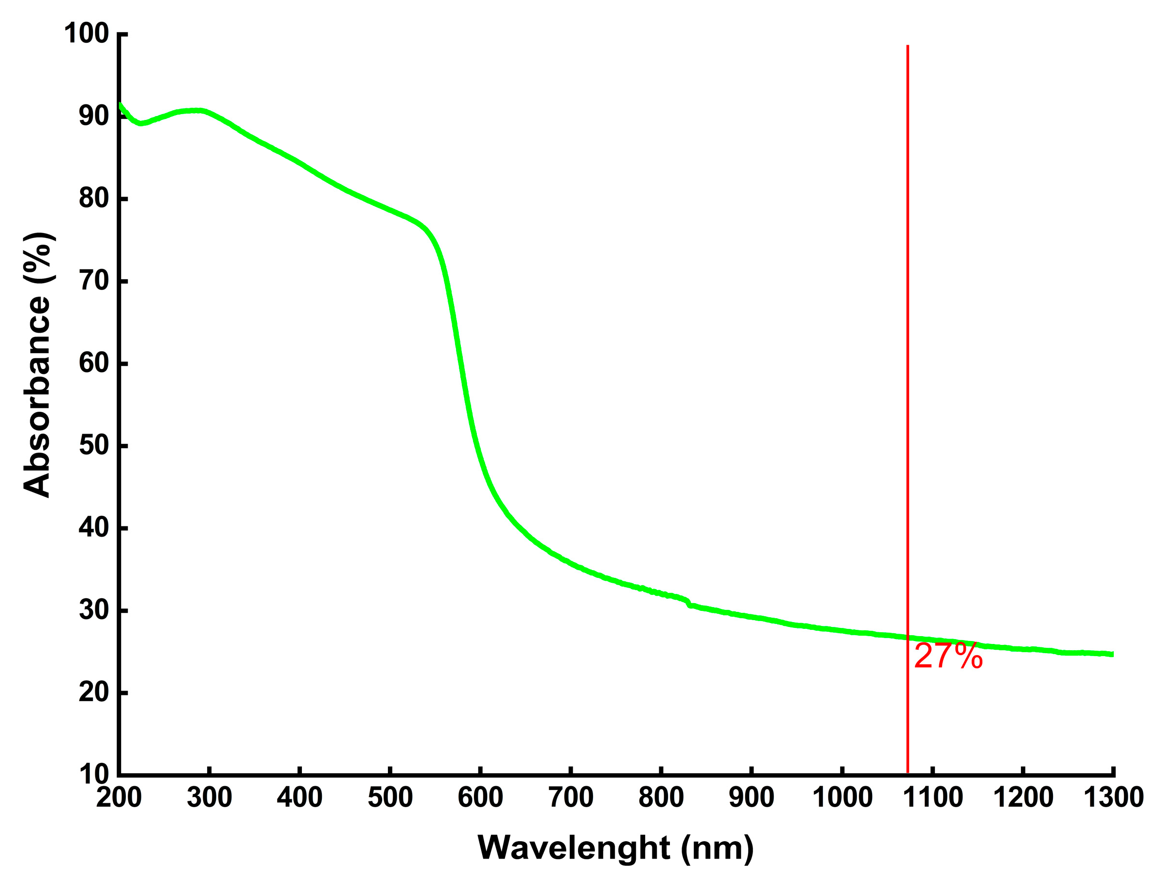
A first preliminary optical characterization of the copper substrate was performed to understand the causes of poor bonding. Figure 4 shows the absorptivity of the substrate, measured in reflection mode over the 400–1200 nm wavelength range, after rendering the solid surface opaque with deep grinding. This surface preparation was carried out because surface roughness strongly influences scattering phenomena [34]. Moreover, it ensures that the substrate roughness is comparable to that of additively manufactured components, maintaining consistency with the reference framework of the present study. A pronounced decrease in absorptivity is observed upon entering the infrared region, with a measured value of 27% at the wavelength of 1070 nm, corresponding to the laser used in processing. This clearly indicates a substantial reduction in melting efficiency, necessitating a higher overall energy input. Moreover, Cu offers an extremely high thermal conductivity of about 300 W/m × K [35], which causes the substrate to behave as a heat sink, further reducing the melting capabilities and inducing considerable residual tension during deposition, ultimately leading to cracking failures. In fact, subsequent tests showed that the increase in the energy input tends to promote solidification cracking rather than mitigating these issues.
Further, Cu is known to lose a significant fraction of its mechanical properties at elevated temperatures; Crosby et al. [36] reported a tensile strength reduction of up to 80% at 500 °C for extruded OFHC Cu bars. Consequently, overheating of the substrate compromises its ability to sustain the residual stresses generated during deposition.
These outcomes suggested the need to develop a peculiar deposition strategy: the approach integrates preheating and interlayer cooling stages, designed both to locally increase absorptivity and to allow recovery of sufficient mechanical strength to withstand thermomechanical stresses. A schematic of the process steps and corresponding parameters is reported in Figure 5. The bonding process was implemented as a multistage deposition strategy. In the initial preheating phase, a small amount of powder was also spread onto the substrate surface, forming a less reflective layer that improved laser absorption and ensured stable melting. The first layer was then deposited with highly energetic parameters to overcome the heat sink effect of copper. A controlled cooling interval of 10 min followed, a value determined through iterative testing (from 2 to 10 min in 1-min increments) to ensure complete recovery of the joint integrity before the deposition of the second layer. This second layer was processed using optimized deposition parameters, after which a longer cooling stage of twice the duration of the first was applied. This 20-min interval resulted from the same incremental optimization procedure and was necessary to fully stabilize the joint. Once this stage was completed, the deposition region was sufficiently distant from the substrate interface, and the process was continued under standard In718 deposition conditions outlined in Table 2.
At this stage, the produced junctions appeared visually free of delamination and exhibited good metallurgical bonding and adhesion. This approach also limited high energetic input only to the first deposition layers, helping to prevent excessive melt-pool temperatures and subsequent material vaporization. The more detailed microstructural analysis presented in the following section further confirms the absence of defects.

3.2. Microstructural Analysis and Phase Transformation

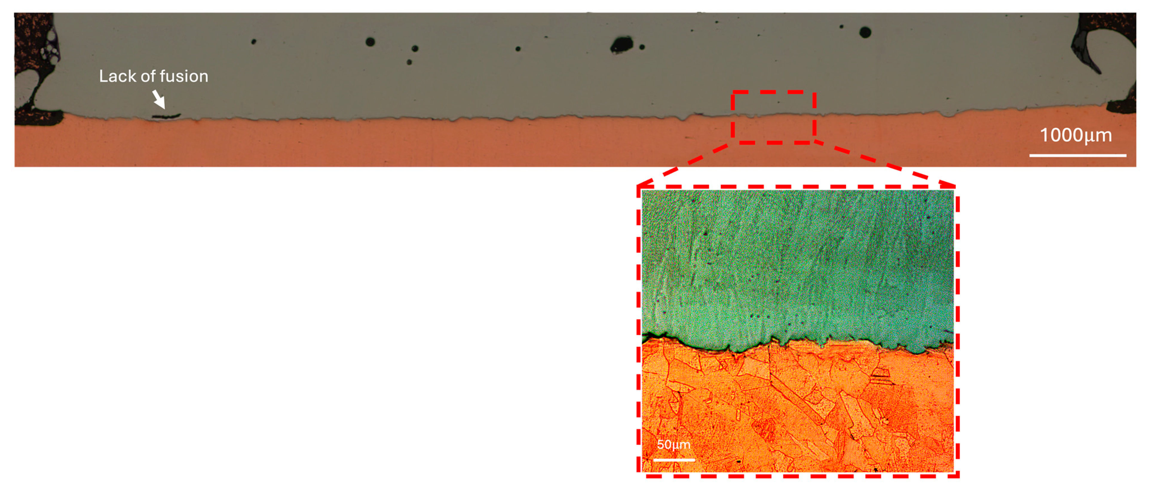
Figure 6 shows OM imaging of the entire deposited cross-section, revealing nearly defect-free bonding. The only exceptions observed were a few small lack-of-fusion defects (indicated by arrows). The first deposited layer also appears free of inherent porosity, whereas the porosity detected in the second layer could be attributed to the large variation in energetic input.
After etching, higher magnification imaging reveals bonding without evidence of mixing-induced brittle phases. However, a pronounced morphological difference is evident between the two material sides.
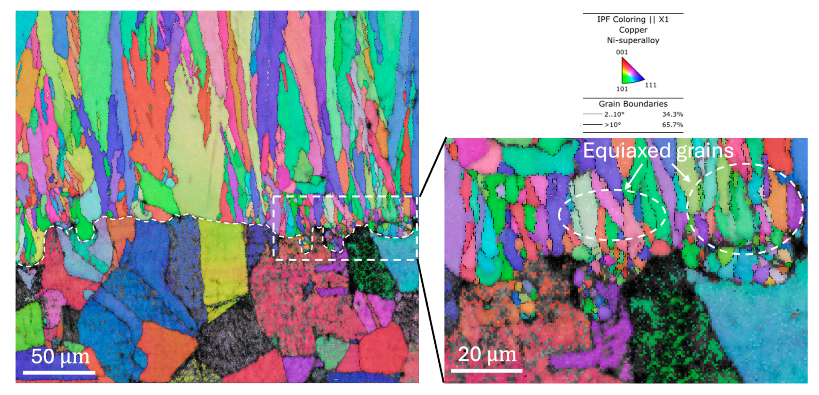
To better understand the morphologies within the fusion zones, an EBSD analysis, shown in Figure 7, was also performed. The results confirmed the absence of epitaxial grain growth in both joints. On the Cu substrate side, directly beneath the interface, large equiaxed grains were observed, which are a typical feature of the extrusion process. A slight elongation along the build direction, however, was also detected, indicating that preheating effectively limited heat dissipation into the copper and suggesting that grain growth was locally stimulated by the higher energy density applied during the deposition of In718.
Immediately above the interface, the deposited In718 displayed fine equiaxed grains, as highlighted in the inset of Figure 7, while, at greater distances from the interface, columnar grains aligned with the build direction were found with average dimensions of 42.7 µm, a value consistent with conventional In718 DED processing. These findings indicate that the thermal influence of the copper substrate vanishes just after the first deposited layer, further demonstrating the effectiveness of the multistage process in reducing the undercooling degree.
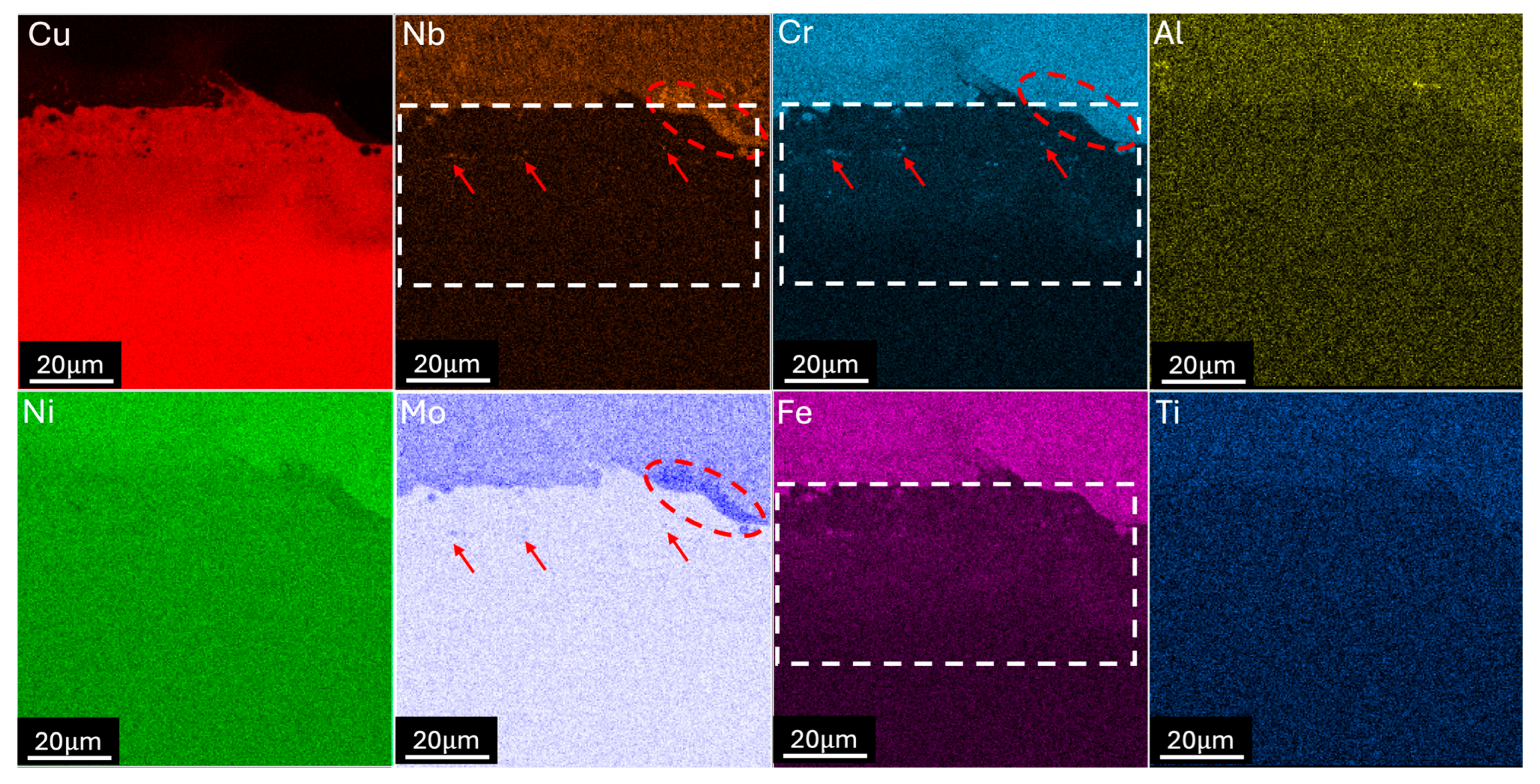
In order to characterize the phase transformation behavior that occurred, at first, EDS analysis was performed (Figure 8), allowing us to distinguish which elements were the main elements involved in the diffusion bonding.
An analysis of the Cu maps reveals a local depletion of copper immediately beyond the interface, confirming that a liquid-state reaction occurred between the two materials. This reaction reached a penetration depth of more than 30 µm and allows the identification of four distinct zones based on morphological and compositional analyses: the interface, the diffusion-affected zone (DAZ), and the two base materials. At a broader scale, as expected, Ni exhibited the highest diffusion due to its well-known metallurgical affinity with Cu, followed by Nb, Cr, and Fe, each reaching penetration depths of approximately 20 µm (Figure 8, white squares). In addition, Nb, Cr, and Mo displayed a pronounced enrichment both directly along the interface (Figure 8, red circle) and within the diffusion zone, where they formed circular submicron-sized islands (Figure 8, red arrows), suggesting the formation of intermetallic compounds. In contrast, Ti and Al were barely detected, indicating their minimal participation in the bonding process.
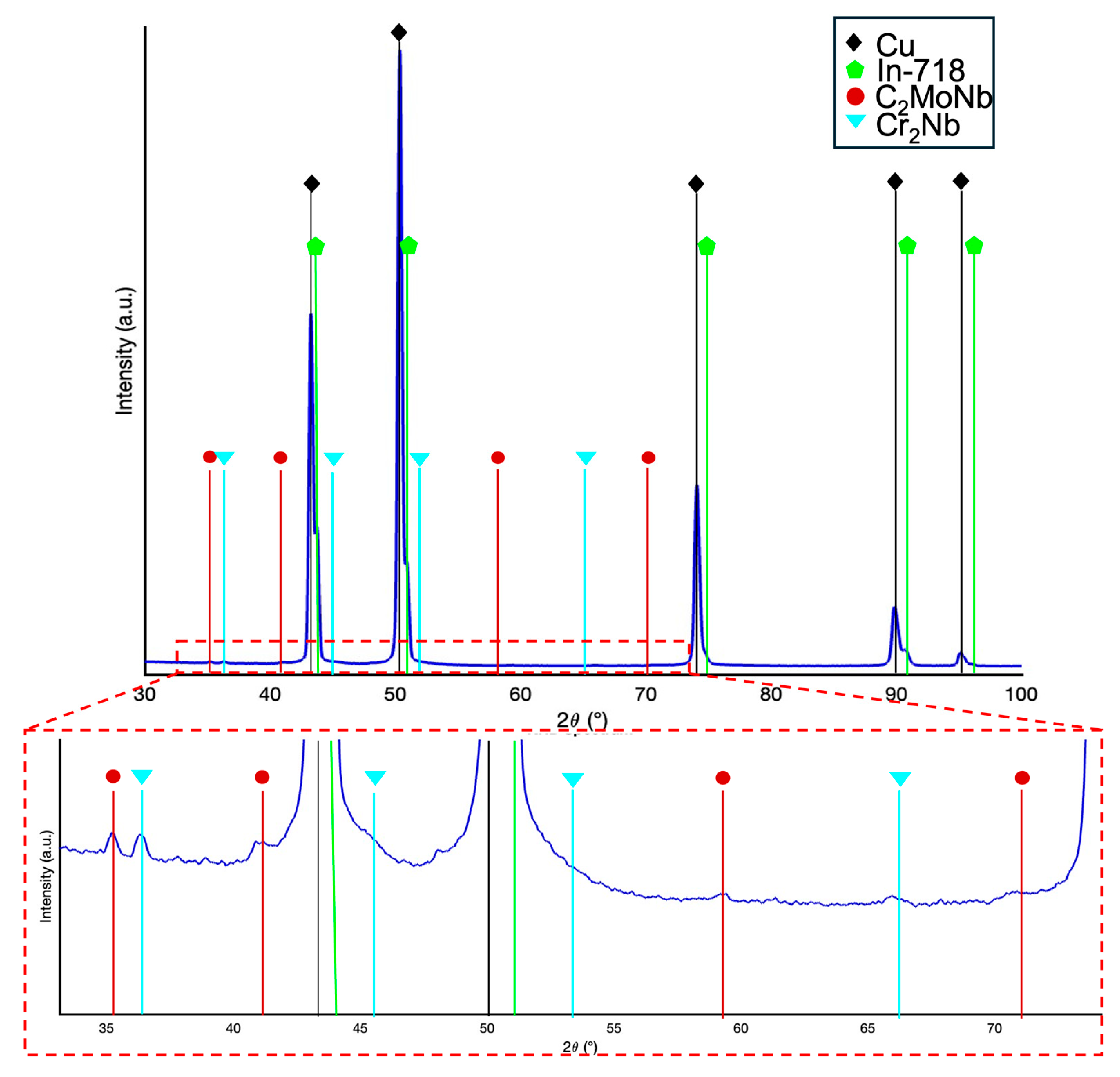
The nature of the newly formed phases was investigated by microdiffraction, as shown in Figure 9. In addition to the characteristic peaks of Cu and Ni, which exhibit the highest intensity, minor phases were also detected within the 2 θ range of 30–70°. Most of these minor peaks are consistent with the presence of FCC C15 Cr2Nb and C2MoNb carbides. The formation of these complex carbides can be attributed to the severe thermal conditions experienced during the initial deposition stages. In718 is known to generate MC-type carbides during solidification, particularly along grain boundaries, through the dissolution of metastable Laves phases within a temperature range of 1265–1280 °C [37,38]. This temperature window aligns with the high-power input required to overcome the reflection issues discussed in Section 3.1. Regarding the C15 FCC Cr2Nb phase, it represents the stable intermetallic form of this compound and is well known for its strengthening effect in a copper matrix. Similar compounds have also been reported by Preis et al. in comparable bimetallic systems [39].

3.3. Hardness Profile and Creep Behavior

To investigate the effect of bonding on the mechanical properties of the material, an initial Vickers microhardness test was performed in the region closest to the interface. The results confirmed that diffusion into the substrate influenced the mechanical response, producing a distinct hardness gradient from the substrate toward the In718 deposition. Specifically, the hardness increased from 55.5 ± 2.4 HV in the substrate to 120.6 ± 7.2 HV in the DAZ, and further to 235.3 HV on the Inconel side.
If the measured hardness is in line with literature results for extruded Cu-based material [40], for the DED-In718 side, further consideration is required. Reported hardness values for DED-In718, in the as-built state, vary a lot depending on processing conditions, with maxima approaching 400 HV [41,42]. However, Muller et al. [43], in a hybrid manufacturing process involving deep rolling, obtained hardness values very similar to those of the present study, attributing the slight reduction in hardness to the microstructural heterogeneity, particularly to the variations in grain size. This explanation is consistent with the local refinement observed along the junction (Figure 7) because of the severe thermal history experienced during processing. Moreover, the increased scatter in hardness values in this region further supports this interpretation.
The role of the newly formed interfacial phases and the effects of diffusion were further examined using nanoindentation on the same regions shown in Figure 8. Nanoindentation provided not only hardness measurements but also the local average stiffness, enabling insights into the nature of the intermetallic and carbide phases formed. The typical triangular indentations produced by the test are clearly visible in Figure 10a, whose size is progressively reduced moving to the In718 side. This aspect is even more evident in the load–displacement curves seen in Figure 10c. The penetration depth was found to vary between 80 and 200 nm, showing the huge difference in the elastic recovery of the two studied materials. Cu, in fact, demonstrated the lowest elastic recovery, which consequently corresponded to the lowest elastic modulus. Interpolating the results, the map of Figure 10b is extracted. The transition of mechanical properties exactly follows the elemental diffusion highlighted by the EDS mapping, confirming that the diffusion zone effectively bridges the properties of the constituent base material. Moreover, it enabled the precise definition of the DAZ and interface dimensions, thereby allowing the evaluation of their averaged properties reported in Figure 10d.
On average, both the elastic modulus and nanohardness at the bonding interface were found to be approximately 10% higher than those of the IN718 base material and about 50% higher than those of the Cu substrate. The newly formed phases in this region, whose possible stoichiometries were proposed in the previous section, are brittle and can significantly influence the hardness response, especially considering their sizes of some tens of microns. In contrast, the DAZ exhibited hardness values only about 22% higher than those of the Cu base material. In this zone, in fact, as revealed by the elemental mapping, the precipitate distribution is much finer and more homogeneous. Regarding the mechanical data, the large discrepancy in strength between IN718 and Cu required the use of relatively low applied loads. On the IN718 side, this condition induced indentation size effects (ISE) due to the local interaction with dislocation, as widely reported in the literature [44]. By relating each extracted property to the indentation depth, a stable hardness value was reached only for penetrations deeper than 100 nm. Consequently, indentations with shallower depths were excluded from the averages. Even with this filtering, the obtained results remain consistent with similar studies carried out on IN718 [45,46,47].
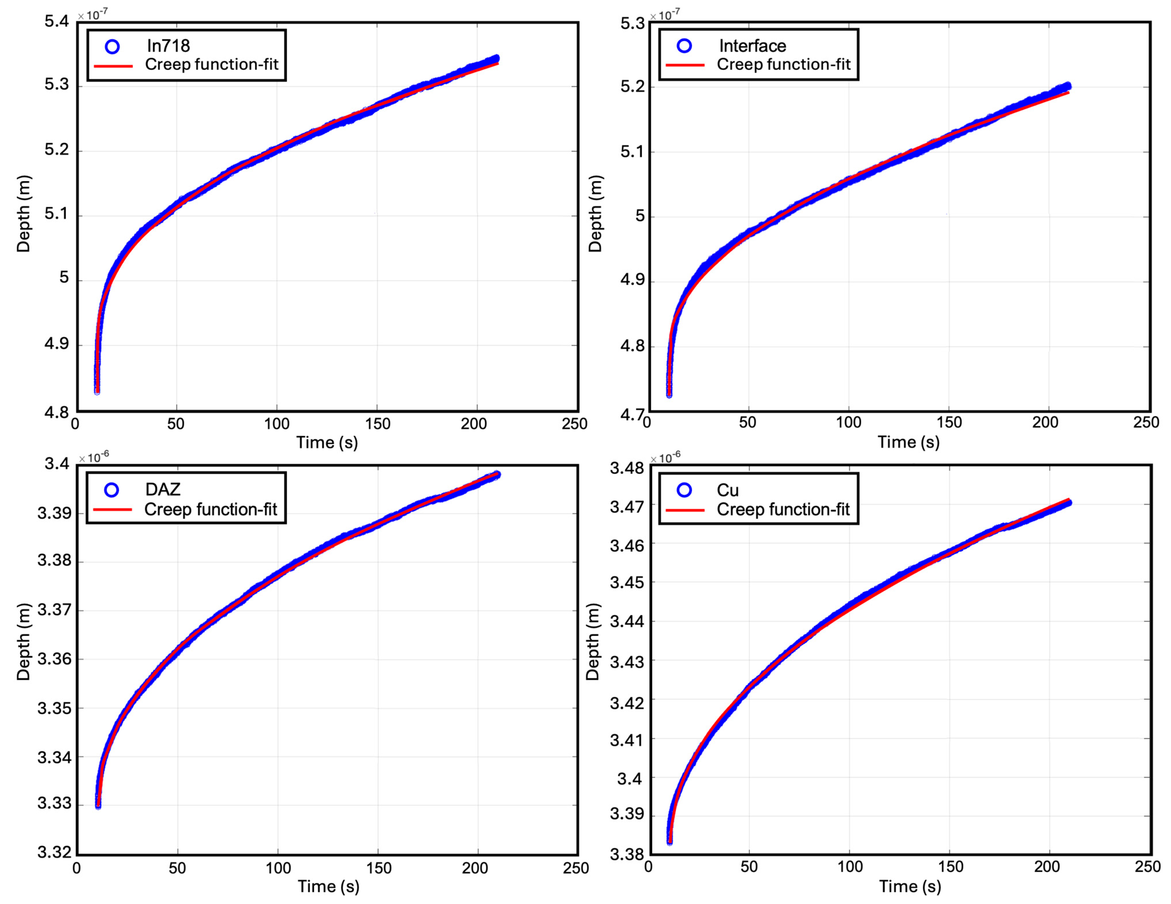
To investigate the creep behavior of the system and extract the constitutive relation, nanoindentations were made with a focus on the holding stage. The fitting of the experimental results obtained during ambient temperature was performed according to Equation (7) with nonlinear least squares fitting (“fit” function in MATLAB R2023b) and is reported in Figure 11, where the red line denotes the fitted curves. In all cases, the indentation depth increases monotonically with time, reflecting time-dependent deformation under constant load, characteristic of creep. The curves exhibit a typical primary-to-secondary creep transition, with a rapid initial increase in depth followed by a gradual reduction in the creep rate as the material approaches a near-steady state. For each material, the fitted curves overlap closely with the experimental data, indicating that the proposed model captures the creep kinetics. The agreement is particularly good in the early stage (t < 50 s), where the indentation depth shows the strongest time dependence. The model also successfully reproduces the more gradual depth evolution at longer holding times with only minimal deviations between experiment and fit, demonstrating both the robustness of the creep formulation and the stability of the fitting procedure. Comparing the four regions, the magnitude of the creep depth varies systematically. The DAZ and Cu substrates exhibit the largest total depth increase, reflecting their lower creep resistance under the applied conditions. In contrast, the In718 and interface zones show comparatively smaller creep depths, consistent with the higher strength and creep resistance expected from Ni-based superalloys and metallurgically bonded interface regions.
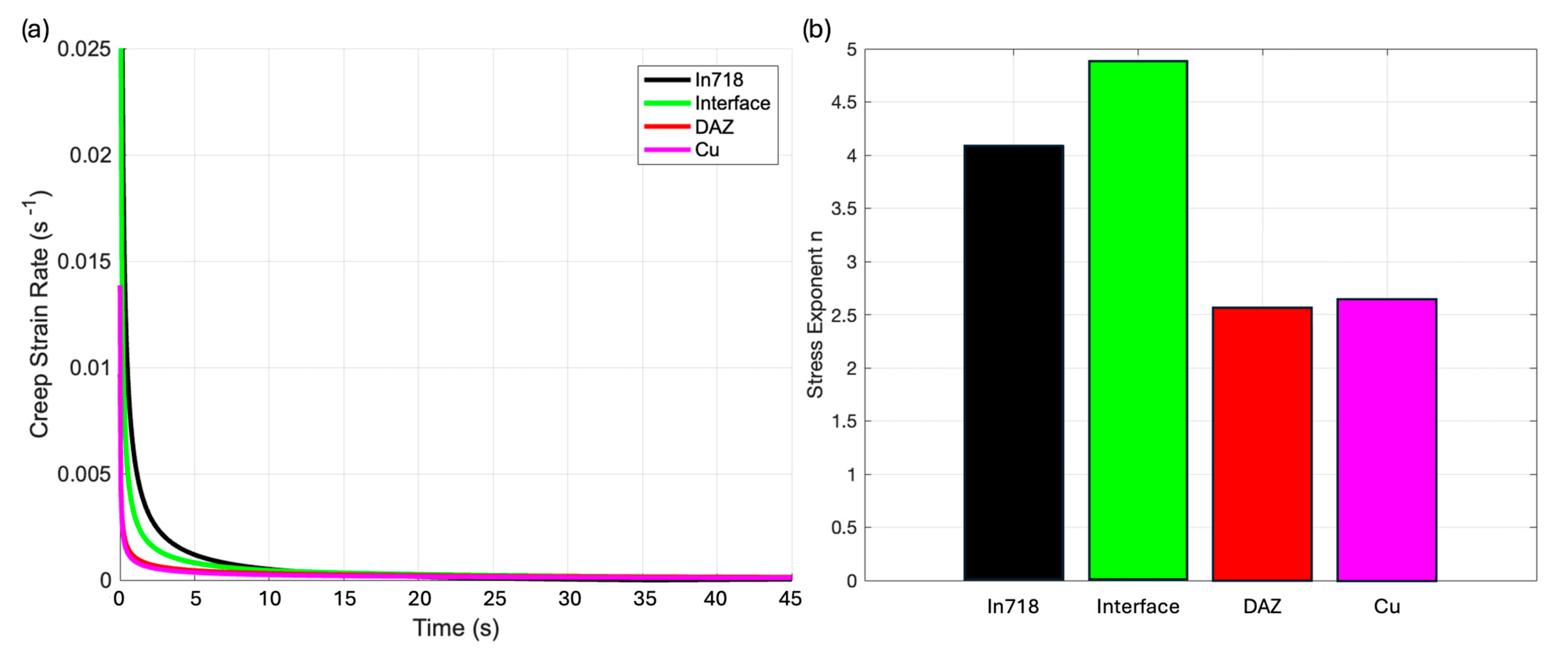
A detailed comparison of the creep behavior of the different zones of the bonding is proposed in Figure 12. Focusing on Figure 12a for all the various bonding zones, a very sharp decrease in the creep strain rate (CSR) can be observed, confirming the occurrence of strain hardening phenomena after the plastic deformation. Moreover, the CSR gradually decreases and rapidly reaches a plateau, marking the onset of steady-state creep. This stage results from the combined effects of strain hardening and recovery occurring in the various zones. By examining the slope of the linear fitting curve that relates stress to CSR, the creep stress exponent (CSE) can be determined. Figure 12b compares the CSE values in the different zones.
Different creep mechanisms can be identified by their characteristic CSE ranges: diffusion creep (CSE ≈ 1–2), grain boundary creep (CSE ≈ 2–3), viscous dislocation motion (CSE ≈ 3–4), and dislocation climb (CSE > 4) [48]. Variations in CSE reflect the differences in creep resistance, with larger exponents signifying stronger resistance to deformation.
A significantly higher CSE, coherent with the dislocation climb mode, is observed on the In718 side, with a peak value at the bonding interface. This enhanced creep resistance, likely linked to the formation of intermetallic compounds, which act as rigid obstacles that hinder dislocation glide and promote dislocation climb, is also supported by the smaller grain sizes characteristic of the first layers of the deposition [49]. On the copper side, instead, grain boundary creep is the dominant mechanism. The larger Cu grains facilitate grain sliding, while the compositional gradients typical of the DAZ increase vacancy concentration and accelerate grain boundary diffusion. In this region, stress gradients generate chemical potential differences across the grain boundaries, activating also a Coble creep mode [50]. These combined factors explain the slightly lower CSE measured in the DAZ, where strong diffusion contributes to grain boundary creep.

3.4. Tensile Behavior

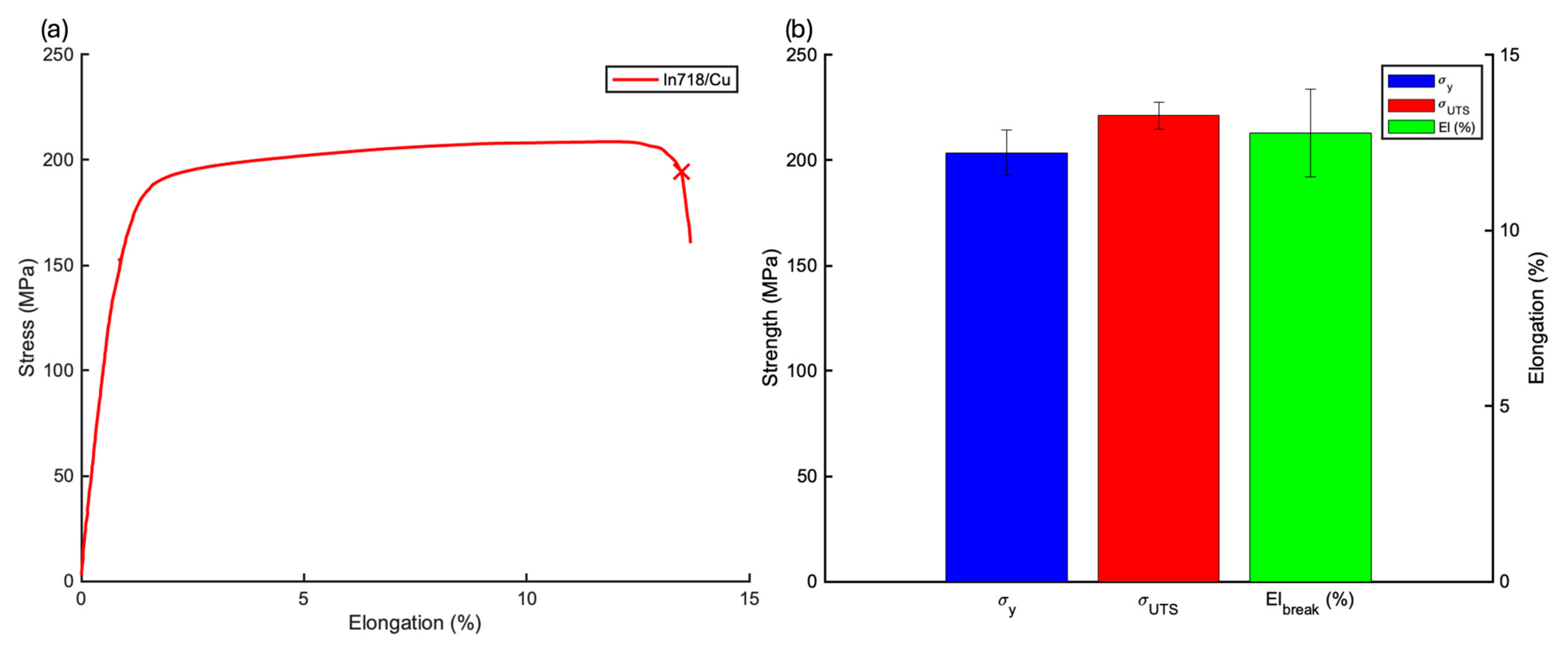
The tensile behavior of the deposited samples was finally investigated and reported in Figure 13. From these experiments, the representative stress–strain curve was extracted, allowing for to measure of the yield strength, the ultimate tensile strength, and both the uniform and total elongation. The difference between these two elongations reflects the strain contribution that arises from localized necking.
All the tested samples were machined along the building direction, and as expected, the fracture was predominantly observed on the Cu side, confirming the strong interfacial bonding. In total, four samples were tested: three fractured within the copper region, while only one exhibited failure directly at the interface.
Consequently, for the as-deposited bimaterial, the mechanical properties were measured as follows: a yield strength (YS) of 204 ± 11 MPa, an ultimate tensile strength (UTS) of 221 ± 7 MPa, a uniform elongation of 5.8 ± 1.7%, and a maximum elongation of 13.4 ± 1.3%.
Although tensile strength values for DED In718 in the as-built condition can reach approximately 600 MPa [32], the relatively low strengths observed in this study are expected, as fracture occurred in the copper region; consequently, the measured properties primarily reflect the mechanical response of the copper-dominated portion of the sample rather than the DED In718. When compared with the literature values for extruded copper, the results are in excellent agreement [51,52].
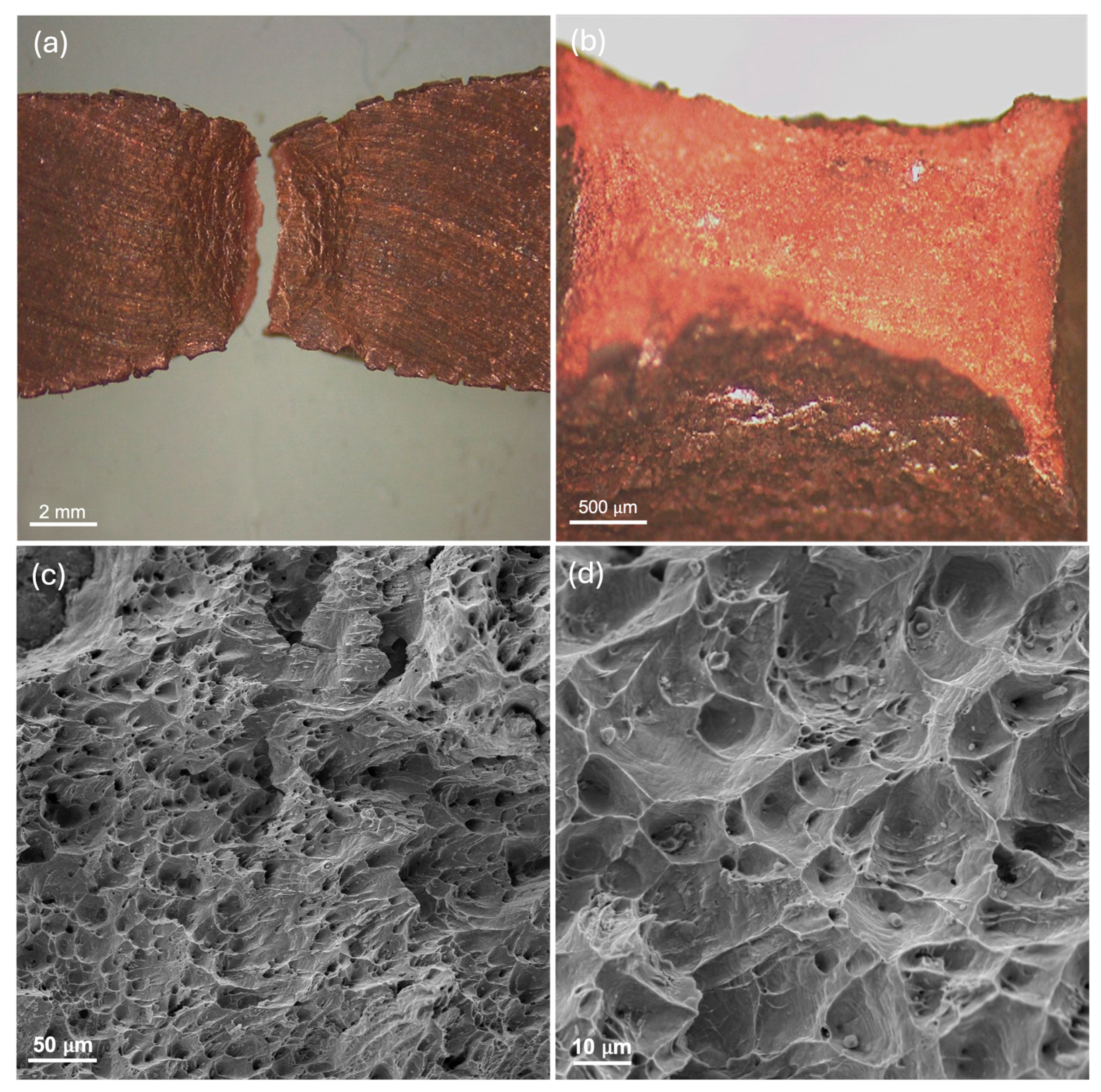
Visual inspection of the tested tensile specimens at a stereoscope magnification degree was first made on the gage section, focusing on the necking region (Figure 14a). The significant reduction in lateral cross-sectional area with the presence of void sheets and shear lip zones (Figure 14b) confirmed localized necking prior to fracture on the Cu side, suggesting that the interfacial bonding strength exceeded the intrinsic strength of Cu. Fractographic analysis of the tensile specimens was conducted using SEM. As shown in Figure 14c, the fracture surface exhibits well-defined dimple structures, characteristic of a ductile failure mode. Step-like features were also observed, indicating crack propagation with 90° directional shifts. These shifts are typically associated with fracture path deviations across heterogeneous microstructural regions, where variations in mechanical resistance deflect the crack front. Not by chance, the examined area corresponds to the region near the interface, where the diffusion positive strengthening gradient was amply demonstrated.
For specimens that exhibited necking close to the junction, on the Cu side, a higher magnification analysis (Figure 14d) also provided further insight into the strengthening mechanisms activated by elemental diffusion. In this region, spherical precipitates often surrounded by circular voids were identified, which is consistent with the Orowan bowing mechanism. Thereby, dislocations are forced to bypass the stable, non-shearable precipitates by bending around them. This bypassing process increases the dislocation line tension and creates additional stress fields, raising the critical resolved shear stress required for plastic deformation and contributing significantly to the observed strengthening in the interfacial region.

4. Conclusions

This study systematically investigates the microstructure and mechanical performance of an additively manufactured bimetallic IN718/Cu produced by DED. The advanced characterization techniques used, including SEM microdiffraction and nanoindentation, provided valuable insights into the structure–property relationships of the bimetallic material. The main conclusion can be summarized as follows:
  • A tailored process enables the formation of a defect-free joint between the two materials. In particular, the preheating and interlayer cooling stages are critical for preserving the mechanical properties of the Cu substrate and overcoming challenges associated with the intrinsic characteristics of the material.
  • Elemental distribution and microdiffraction analyses indicate that liquid-state reactions and solid-state diffusion can penetrate to depths exceeding 30 µm, promoting the formation of metastable C15-Cr2Nb and Mo-Cr-Nb intermetallic phases, as well as complex carbides.
  • The influence of the reaction zone on joint brittleness was assessed by nanoindentation, revealing a positive gradient of mechanical properties from the substrate to the In718 deposition. The peak hardness was recorded precisely at the interface, where intermetallic compounds reached their largest size (tens of microns). In contrast, the DAZ exhibited a more controlled and uniform hardening response, with secondary phases more homogeneously distributed. This highlights the strong correlation between precipitate size and hardening behavior.
  • The creep behavior was investigated by nanoindentation creep, focusing on the holding stage, revealing the highest creep resistance at the bonding interface and the greatest creep susceptibility within DAZ. Two distinct creep mechanisms were identified on opposite sides of the joint: dislocation climb on the In718 side and grain boundary creep on the copper side. To further validate these interpretations, future work should include high-temperature nanoindentation and complementary uniaxial creep tests to more directly probe the operative deformation mechanisms.
  • Tensile tests confirmed that the interfacial bonding strength exceeds the intrinsic strength of the Cu substrate, as fractures occurred exclusively on the Cu side and were accompanied by consistent necking phenomena. Fractographic analysis provided insights into the underlying strengthening mechanism, which is consistent with Orowan bowing, as supported by the significant hardness contrast with the matrix.
Future research should also focus on optimizing processing parameters with the involvement of structural Cu-Cr alloys like the GrCop family and exploring post-processing treatments to further enhance the mechanical properties of the bimetallic functional component. Moreover, a complete thermal characterization is required to evaluate the impact of the diffusion bonding on the thermal properties.

Author Contributions

Conceptualization, P.F., F.B., and A.A.; Methodology, S.F. and A.A.; Software, S.F.; Validation, S.F., J.V., and A.Z.; Formal Analysis, S.F., F.B., and A.A.; Investigation, S.F., J.V., and A.Z.; Resources, P.F. and F.B.; Data Curation, S.F., J.V., A.Z., and A.A.; Writing—original draft preparation, S.F.; Writing—review and editing, P.F., F.B., and A.A.; Visualization, S.F., J.V., and A.Z.; Supervision, A.A. and F.B.; Project administration, F.B.; Funding acquisition, P.F. and F.B. All authors have read and agreed to the published version of the manuscript.

Funding

This study was carried out within the MICS (Made in Italy—Circular and Sustainable) Extended Partnership and received funding from the European Union Next-Generation EU (PIANO NAZIONALE DI RIPRESA E RESILIENZA (PNRR)—MISSIONE 4 COMPONENTE 2, INVESTIMENTO 1.3—D.D. 1551.11-10-2022, PE00000004). This manuscript reflects only the authors’ views and opinions; neither the European Union nor the European Commission can be considered responsible for them.

Data Availability Statement

The original contributions presented in this study are included in the article. Further inquiries can be directed to the corresponding author.

Acknowledgments

All authors thank the initiative PNRR Partenariato Esteso for providing funding to Politecnico Di Torino under MICS “Circular & Sustainable Made in Italy”—PE00000004—CUP E13C22001900001. Also, all authors would like to express their gratitude to Consorzio Hypatia for the support.

Conflicts of Interest

The authors declare no conflicts of interest.

References

  1. Arnold, R.; Suslov, D.I.; Haidn, O.J. Experimental Investigation of Film Cooling with Tangential Slot Injection in a LOX/CH4 Subscale Rocket Combustion Chamber. Trans. JSASS Space Technol. Jpn. 2009, 7, 81–86. [Google Scholar] [CrossRef]
  2. Haidn, O. Advanced Rocket Engines. In Advances in Propulsion Technology for High-Speed Aircraft; Research & Technology Organisation (RTO): Neuilly-sur-Seine, France, 2007; pp. 6.1–6.40. [Google Scholar]
  3. Ellis, D.L. GRCop-84: A High-Temperature Copper Alloy for High-Heat-Flux Applications; Bibliogov: Asheville, NC, USA, 2005. [Google Scholar]
  4. De Groh, H.C.; Ellis, D.L.; Loewenthal, W.S. Comparison of GRCop-84 to Other Cu Alloys with High Thermal Conductivities. J. Mater. Eng. Perform. 2008, 17, 594–606. [Google Scholar] [CrossRef]
  5. Poudel, A.; Gradl, P.R.; Shao, S.; Shamsaei, N. Tensile Deformation Behavior of Laser Powder Direct Energy Deposited Inconel 625: Cryogenic to Elevated Temperatures. Mater. Sci. Eng. A 2024, 889, 145826. [Google Scholar] [CrossRef]
  6. Wei, C.; Zhang, Z.; Cheng, D.; Sun, Z.; Zhu, M.; Li, L. An Overview of Laser-Based Multiple Metallic Material Additive Manufacturing: From Macro- to Micro-Scales. Int. J. Extrem. Manuf. 2021, 3, 012003. [Google Scholar] [CrossRef]
  7. Carroll, B.E.; Otis, R.A.; Borgonia, J.P.; Suh, J.; Dillon, R.P.; Shapiro, A.A.; Hofmann, D.C.; Liu, Z.-K.; Beese, A.M. Functionally Graded Material of 304L Stainless Steel and Inconel 625 Fabricated by Directed Energy Deposition: Characterization and Thermodynamic Modeling. Acta Mater. 2016, 108, 46–54. [Google Scholar] [CrossRef]
  8. Sahasrabudhe, H.; Harrison, R.; Carpenter, C.; Bandyopadhyay, A. Stainless Steel to Titanium Bimetallic Structure Using LENSTM. Addit. Manuf. 2015, 5, 1–8. [Google Scholar] [CrossRef]
  9. Gualtieri, T.; Bandyopadhyay, A. Niobium Carbide Compostie Coatings on SS304 Using Laser Engineered Net Shaping (LENSTM). Mater. Lett. 2017, 189, 89–92. [Google Scholar] [CrossRef]
  10. Gradl, P.R.; Protz, C.; Fikes, J.; Ellis, D.; Evans, L.; Clark, A.; Miller, S.; Hudson, T. Lightweight Thrust Chamber Assemblies Using Multi-Alloy Additive Manufacturing and Composite Overwrap. In Proceedings of the AIAA Propulsion and Energy 2020 Forum; American Institute of Aeronautics and Astronautics, Virtual Event, 24 August 2020. [Google Scholar]
  11. Gradl, P.R.; Protz, D.C.S.; Ellis, D.D.L.; Greene, S.E. Progress in Additively Manufactured Copper-Alloy GRCop-84, GRCop-42, and Bimetallic Combustion Chambers for Liquid Rocket Engines. In Proceedings of the International Astronautical Congress, Washington, DC, USA, 21–25 October 2019. [Google Scholar]
  12. Clark, A.; Hudson, T.; Miller, S.; Edrington, S.; Park, C.; Protz, C. Lightweight Thrust Chamber Composite Overwrap Lessons Learned. In Proceedings of the CAMX-The Composites and Advanced Materials Expo, Dallas, TX, USA, 19–21 October 2021. [Google Scholar]
  13. Gradl, P.R.; Teasley, T.W.; Protz, C.S.; Garcia, M.B.; Ellis, D.; Kantzos, C. Advancing GRCop-Based Bimetallic Additive Manufacturing to Optimize Component Design and Applications for Liquid Rocket Engines. In Proceedings of the AIAA Propulsion and Energy 2021 Forum; American Institute of Aeronautics and Astronautics, Virtual Event, 9 August 2021. [Google Scholar]
  14. Turchanin, M.A.; Agraval, P.G.; Abdulov, A.R. Phase Equilibria and Thermodynamics of Binary Copper Systems with 3d-Metals. VI. Copper-Nickel System. Powder Met. Met. Ceram. 2007, 46, 467–477. [Google Scholar] [CrossRef]
  15. Stavropoulos, P.; Foteinopoulos, P. Modelling of Additive Manufacturing Processes: A Review and Classification. Manuf. Rev. 2018, 5, 2. [Google Scholar] [CrossRef]
  16. Liu, M.; Kumar, A.; Bukkapatnam, S.; Kuttolamadom, M. A Review of the Anomalies in Directed Energy Deposition (DED) Processes & Potential Solutions—Part Quality & Defects. Procedia Manuf. 2021, 53, 507–518. [Google Scholar] [CrossRef]
  17. Kou, S. Welding Metallurgy; John Wiley & Sons, Incorporated: Hoboken, NJ, USA, 2002; ISBN 0-471-43491-4. [Google Scholar]
  18. Preis, J.; Wang, Z.; Howard, J.; Lu, Y.; Wannenmacher, N.; Shen, S.; Paul, B.K.; Pasebani, S. Effect of Laser Power and Deposition Sequence on Microstructure of GRCop42—Inconel 625 Joints Fabricated Using Laser Directed Energy Deposition. Mater. Des. 2024, 241, 112944. [Google Scholar] [CrossRef]
  19. Iams, A.D.; Lienert, T.J.; Otazu, D.A.; Ramoni, M. Effects of Deposition Sequence on Microstructural Evolution in Additively Manufactured Cu-Cr-Nb Alloy / Superalloy Bimetallic Structures. Addit. Manuf. Lett. 2023, 6, 100151. [Google Scholar] [CrossRef]
  20. Anderson, R.; Terrell, J.; Schneider, J.; Thompson, S.; Gradl, P. Characteristics of Bi-Metallic Interfaces Formed During Direct Energy Deposition Additive Manufacturing Processing. Met. Mater. Trans. B 2019, 50, 1921–1930. [Google Scholar] [CrossRef]
  21. Hales, S.J.; Domack, C.S.; Taminger, K.M. Electron Beam Freeform Fabrication of Dissimilar Materials: Cracking in Inconel® 625 Deposited on GRCop-84; Bibliogov: Asheville, NC, USA, 2020. [Google Scholar]
  22. Kassner, M.E.; Son, K.T.; Lee, K.A.; Kang, T.-H.; Ermagan, R. The Creep and Fracture Behavior of Additively Manufactured Inconel 625 and 718. Mater. High. Temp. 2022, 39, 499–506. [Google Scholar] [CrossRef]
  23. Onuike, B.; Heer, B.; Bandyopadhyay, A. Additive Manufacturing of Inconel 718—Copper Alloy Bimetallic Structure Using Laser Engineered Net Shaping (LENSTM). Addit. Manuf. 2018, 21, 133–140. [Google Scholar] [CrossRef]
  24. B09 Committee ASTM International. Test Method for Density of Powder Metallurgy (PM) Materials Containing Less Than Two Percent Porosity; ASM International: Materials Park, OH, USA, 2008. [Google Scholar] [CrossRef]
  25. E04 Committee. Test Method for Microindentation Hardness of Materials; ASTM International: West Conshohocken, PA, USA, 2022. [Google Scholar]
  26. BSI Standards Limited. Metallic Materials. Instrumented Indentation Test for Hardness and Materials Parameters Test Method; Under Review; BSI Standards Limited: London, UK, 2015; ISBN 978-0-580-75794-5. [Google Scholar]
  27. Oliver, W.C.; Pharr, G.M. Measurement of Hardness and Elastic Modulus by Instrumented Indentation: Advances in Understanding and Refinements to Methodology. J. Mater. Res. 2004, 19, 3–20. [Google Scholar] [CrossRef]
  28. Gale, J.D.; Achuthan, A. The Effect of Work-Hardening and Pile-up on Nanoindentation Measurements. J. Mater. Sci. 2014, 49, 5066–5075. [Google Scholar] [CrossRef]
  29. Feng, G.; Ngan, A.H.W. Effects of Creep and Thermal Drift on Modulus Measurement Using Depth-sensing Indentation. J. Mater. Res. 2002, 17, 660–668. [Google Scholar] [CrossRef]
  30. Mayo, M.J.; Siegel, R.W.; Liao, Y.X.; Nix, W.D. Nanoindentation of Nanocrystalline ZnO. J. Mater. Res. 1992, 7, 973–979. [Google Scholar] [CrossRef]
  31. E28 Committee. Test Methods for Tension Testing of Metallic Materials; ASTM International: West Conshohocken, PA, USA, 2011. [Google Scholar]
  32. Cavalcante, T.R.F.; Bon, D.G.; Pascoal, C.V.P.; Mariani, F.E.; Faria, G.; Coelho, R.T.; Muñoz, J.A.; Muñoz, J.C.; Cabrera, J.M.; Avila, J.A. As-Built Microstructure and Mechanical Behavior of Inconel 718 Processed via Directed Energy Deposition with Laser Beam. Prog. Addit. Manuf. 2025, 10, 7589–7607. [Google Scholar] [CrossRef]
  33. Liu, Z.; Wang, X.; Kim, H.; Zhou, Y.; Cong, W.; Zhang, H. Investigations of Energy Density Effects on Forming Accuracy and Mechanical Properties of Inconel 718 Fabricated by LENS Process. Procedia Manuf. 2018, 26, 731–739. [Google Scholar] [CrossRef]
  34. Peiponen, K.-E.; Tsuboi, T. Metal Surface Roughness and Optical Reflectance. Opt. Laser Technol. 1990, 22, 127–130. [Google Scholar] [CrossRef]
  35. Simon, N.J.; Drexler, E.S.; Reed, R.P. Properties of Copper and Copper Alloys at Cryogenic Temperatures, 1st ed.; National Institute of Standards and Technology: Gaithersburg, MD, USA, 1992; p. NIST MONO 177.
  36. Crosby, R.L.; Desy, D.H. Dispersion-Strengthening in Copper-Alumina and Copper-Yttria Alloys; Report of Investigations/Bureau of Mines; U.S. Department of the Interior, Bureau of Mines: Washington, DC, USA, 1969; Volume 7266.
  37. Schneider, J.; Farris, L.; Nolze, G.; Reinsch, S.; Cios, G.; Tokarski, T.; Thompson, S. Microstructure Evolution in Inconel 718 Produced by Powder Bed Fusion Additive Manufacturing. J. Manuf. Mater. Process. 2022, 6, 20. [Google Scholar] [CrossRef]
  38. Saumitra, V. Microstructural Evolution and Precipitation Kinetics of Carbides in L-PBF Processed Inconel 718 during Long-Term Homogenization. Mater. Today Commun. 2025, 42, 111192. [Google Scholar] [CrossRef]
  39. Preis, J.; Xu, D.; Paul, B.K.; Eschbach, P.A.; Pasebani, S. Effect of Liquid Miscibility Gap on Defects in Inconel 625–GRCop42 Joints through Analysis of Gradient Composition Microstructure. J. Manuf. Mater. Process. 2024, 8, 42. [Google Scholar] [CrossRef]
  40. Bazaz, B.; Zarei-Hanzaki, A.; Fatemi-Varzaneh, S.M. Hardness and Microstructure Homogeneity of Pure Copper Processed by Accumulative Back Extrusion. Mater. Sci. Eng. A 2013, 559, 595–600. [Google Scholar] [CrossRef]
  41. Wang, Y.; Shi, J. Microstructure and Properties of Inconel 718 Fabricated by Directed Energy Deposition with In-Situ Ultrasonic Impact Peening. Met. Mater. Trans. B 2019, 50, 2815–2827. [Google Scholar] [CrossRef]
  42. Yeoh, Y.C.; Macchi, G.; Jain, E.; Gaskey, B.; Raman, S.; Tay, G.; Verdi, D.; Patran, A.; Grande, A.M.; Seita, M. Multiscale Microstructural Heterogeneity and Mechanical Property Scatter in Inconel 718 Produced by Directed Energy Deposition. J. Alloys Compd. 2021, 887, 161426. [Google Scholar] [CrossRef]
  43. Müller, C.J.; Büßenschütt, K.; Schwedt, A.; Schleifenbaum, J.H.; Sudmanns, M. Enabling Tailored Microstructures by Hybrid Directed Energy Deposition Processing of a Nickel-Based Superalloy. Addit. Manuf. Lett. 2024, 11, 100248. [Google Scholar] [CrossRef]
  44. Elmustafa, A.A.; Stone, D.S. Nanoindentation and the Indentation Size e’ect: Kinetics of Deformation and Strain Gradient Plasticity. J. Mech. Phys. Solids 2003, 51, 357–381. [Google Scholar] [CrossRef]
  45. Profitiliotis, T.; Kladovasilakis, N.; Giarmas, E.; Pechlivani, E.M.; Tzetzis, D. Mechanical Performance and Microstructural Characterization of Additive Manufactured Selective Laser Melted Bimetallic IN718/17-4 PH Stainless Steel. Mater. Sci. Eng. A 2025, 930, 148158. [Google Scholar] [CrossRef]
  46. Khan, S.; Junaid, M.; Khan, F.N. Nanoindentation and Indentation Creep Analysis of Diffusion Bonded of Inconel 718 and AISI 304L Stainless Steel Joint Interface. Proc. Inst. Mech. Eng. Part L J. Mater. Des. Appl. 2025, 239, 1620–1632. [Google Scholar] [CrossRef]
  47. Jiang, R.; Mostafaei, A.; Pauza, J.; Kantzos, C.; Rollett, A.D. Varied Heat Treatments and Properties of Laser Powder Bed Printed Inconel 718. Mater. Sci. Eng. A 2019, 755, 170–180. [Google Scholar] [CrossRef]
  48. Wu, X.; Liu, R.; Khelfaoui, F. Creep Phenomena, Mechanisms, and Modeling of Complex Engineering Alloys. Modelling 2024, 5, 819–840. [Google Scholar] [CrossRef]
  49. Nix, W.D.; Ilschner, B. Mechanisms Controlling Creep of Single Phase Metals and Alloys. Strength. Met. Alloys 1979, 3, 1503–1530. [Google Scholar] [CrossRef]
  50. Chen, Y.; Schuh, C.A. Coble Creep in Heterogeneous Materials: The Role of Grain Boundary Engineering. Phys. Rev. B 2007, 76, 064111. [Google Scholar] [CrossRef]
  51. Atefi, S.; Parsa, M.H.; Ahmadkhaniha, D.; Zanella, C.; Jafarian, H.R. A Study on Microstructure Development and Mechanical Properties of Pure Copper Subjected to Severe Plastic Deformation by the ECAP-Conform Process. J. Mater. Res. Technol. 2022, 21, 1614–1629. [Google Scholar] [CrossRef]
  52. Zhang, T.; Wang, Z.; Wang, Y.; Chen, Z. Experimental Study on the Mechanical Properties of Oxygen-Free Copper Used in High Energy Physics Detectors and Accelerators. Nucl. Instrum. Methods Phys. Res. Sect. A Accel. Spectrometers Detect. Assoc. Equip. 2019, 935, 8–16. [Google Scholar] [CrossRef]
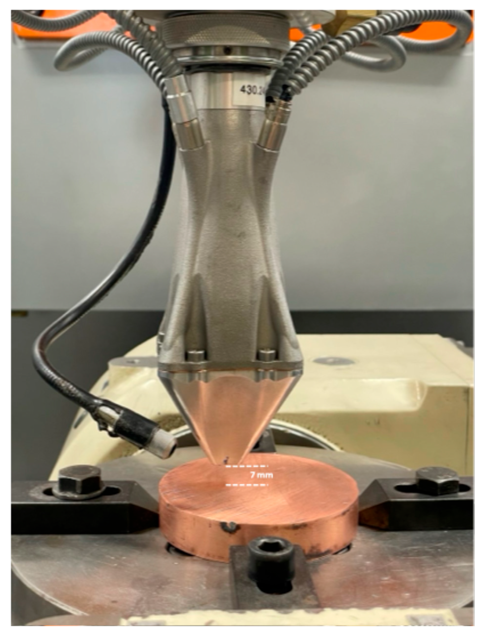
Figure 1. Prima Additive Laserdyne 795 with the REAL_DEDâ coaxial deposition head featuring a laser spot of 2 mm in a 7 mm working distance.
Metals 15 01292 g001
Figure 2. (a) Schematic representation of the massive deposition used to extract tensile samples; (b) tensile sample size selected for the test according to the ASTM E8M; (c) photo of the real tensile sample prior to testing.
Metals 15 01292 g002
Figure 3. Unsuccessful preliminary joining trials: (a) Complete lack of adhesion caused by balling phenomena in the first layer; (b) progressive delamination occurring during deposition.
Metals 15 01292 g003
Figure 4. Optical absorptivity plot of the copper surface after superficial grinding with abrasive papers.
Metals 15 01292 g004
Figure 5. Schematic representation of the multistage deposition strategy and corresponding processing parameters used for bonding In718 onto copper, enabling the production of crack-free samples.
Metals 15 01292 g005
Figure 6. OM cross-section of the investigated cubic deposition, reporting the absence of cracks and defects along the entire cross-section analyzed.
Metals 15 01292 g006
Figure 7. EBSD crystal orientation maps of In718 deposited on a Cu substrate. The dashed lines indicate the bead cross-section outlines and mark the position of the interface. In the inset, the peculiar equiaxed morphology of the diffusion zone is highlighted.
Metals 15 01292 g007
Figure 8. EDS mapping of the diffusion–bonded interface showing the primary elements involved in interdiffusion, as well as regions of local enrichment indicative of intermetallic compound formation.
Metals 15 01292 g008
Figure 9. Microdiffraction analysis of a representative area of 500 mm2 along the diffusion-affected zone. The main intensity peak of the base materials is present, as well as minor peaks of C15 Cr2Nb Laves formation and (Mo, Nb)-C complex carbides.
Metals 15 01292 g009
Figure 10. Nanoindentation mapping of the interface: (a) Indentation shape; (b) interpolated hardness values in the area 75 × 75 mm2 area tested; (c) load–depth curve of the various characteristic zones of the joint; (d) average hardness and elastic modulus of the characteristic areas.
Metals 15 01292 g010
Figure 11. Comparison between fitted and experimental curves for various bonding zones of the In718/Cu system.
Metals 15 01292 g011
Figure 12. (a) Creep strain rate vs. time; (b) stress exponent for the various bonding zones of the In718/Cu joint.
Metals 15 01292 g012
Figure 13. Tensile properties of the In718/Cu diffusion bonding: (a) Representative engineering stress–strain curve of the bimaterial system; (b) tensile strength, including YS and UTS, and strain summary.
Metals 15 01292 g013
Figure 14. Post-test inspection of the tensile specimen: (a) Stereomicroscope image of the gauge length, highlighting pronounced necking and the characteristic ductile ‘cup-and-cone’ fracture; (b) stereomicroscope image of the reduced cross-sectional area, showing consistent shear lip zones; (c) SEM fracture surface images revealing void sheets and step-like features, indicative of a 90° directional shift across the layer boundary; (d) high-magnification SEM image of crack surface occurring on DAZ, showing circular voids and residual inclusions.
Metals 15 01292 g014
Table 1. Chemical composition of Mimete Venus 718â powder conforms to In718 standards.
Element wt.%CCrNiFeMoNb + TaCoAlSiTi
Result0.0719.253.72Bal.3.224.980.10.490.060.87
Table 2. Optimal processing parameters for stable In718 depositions.
P [W]v [mm/min]Δz [mm]f [g/min]Ov. [%]Rel. Density
8506600.57.750%99.78%
Disclaimer/Publisher’s Note: The statements, opinions and data contained in all publications are solely those of the individual author(s) and contributor(s) and not of MDPI and/or the editor(s). MDPI and/or the editor(s) disclaim responsibility for any injury to people or property resulting from any ideas, methods, instructions or products referred to in the content.