Article

Structure and Properties of Al-Co-Cr-Fe-Ni High-Entropy Alloy Subjected to Electron–Ion Plasma Treatment

1
Institute of High Current Electronics SB RAS, 634055 Tomsk, Russia
2
Department of Natural Sciences, Siberian State Industrial University, 654007 Novokuznetsk, Russia
*
Author to whom correspondence should be addressed.
Metals 2022, 12(11), 1987; https://doi.org/10.3390/met12111987
Submission received: 29 September 2022 / Revised: 13 November 2022 / Accepted: 18 November 2022 / Published: 20 November 2022

Abstract

:
High-entropy alloys (HEAs) are a new class of materials consisting of at least five elements in equiatomic or near-equiatomic ratio. HEAs are subjected to various types of surface treatment to improve their properties. One of the most promising methods of surface hardening is electron beam processing. This study aims to examine the structure, elemental, and phase composition of the AlCrFeCoNi HEA surface layer after the deposition of a (B + Cr) film and irradiation with a pulsed electron beam. HEA samples of non-equiatomic composition (33.4 Al; 8.3 Cr; 17.1 Fe; 5.4 Co; 35.7 Ni, at. %), fabricated by wire-arc additive manufacturing (WAAM), were used as study objects. Modification of the HEA surface layer was carried out by a complex method combining deposition of (B + Cr) film samples on the surface and irradiation with a pulsed electron beam in an argon medium. The mode of modification was identified. It makes it possible to increase microhardness (almost two times) and wear resistance (more than five times), reduce the friction coefficient of the HEA surface layer by 1.3 times due to the decrease in the average grain size, formation of particles of borides and oxyborides of complex elemental composition, the introduction of boron atoms into the crystal lattice of HEA.

1. Introduction

High-entropy alloys (HEAs) are a new class of materials consisting of at least five elements in equiatomic or near-equiatomic ratio, which provide them with unique properties as compared to conventional alloys [1]. The HEA concept is based on the idea that a high entropy of mixing can facilitate the formation of stable single-phase microstructures [2], which does not contradict the phase rule based on the laws of thermodynamics. It aroused unprecedented worldwide interest in the development and research of HEA. In this direction, [3] should be considered the first study, in which the atomic concentration of the elements making up the HEA ranges from 5 to 35%. Features of the chemical composition and structure of HEAs lead to the so-called core effects, which determine the unique set of properties of these materials [4,5,6,7]: high entropy effect, strong lattice distortion effect, delayed diffusion effect, and “cocktail” effect. The first effect is that the decrease in entropy upon transition to a more ordered state outweighs the decrease in enthalpy due to the effect of ordered phase formation [2,8]. The lattice distortion effect, as is clear from the definition, is due to the fact that atoms of different sizes randomly occupy interstices in the crystal lattice. Obviously, larger atoms will be located at the maximum distance from each other, since in this case the distortions of the crystal structure and the energy of the system will decrease. The delayed diffusion effect is associated with the influence of lattice distortions, as well as with the formation of nanosized inclusions and amorphous multicomponent phases in various ways of obtaining HEA [2,9,10,11,12,13,14]. This effect is of great practical importance, since, for example, corrosion resistance depends on the diffusion rate. There is no rigorous definition of the “cocktail” effect; it usually means the ability of an alloy to exhibit properties that are not characteristic of each of its components separately [2,4]. As a rule, HEA has properties that exceed the sum of the properties of all its components. Generalization of extensive original results, analysis of HEAs properties, and prospects for their application are provided in [1,15,16].
In the last five years, despite a great number of publications on HEA and the existing serious problems analyzed in [1,2,15,16], two fundamentally new directions in the physics of high-entropy alloys have emerged: improvement of surface properties by depositing thin coatings and films and HEA surfaces modification by different treatment techniques. Among the numerous methods for depositing films or coatings from HEA, it is necessary to consider four of them with a number of advantages: magnetron sputtering [17], thermal sputtering [18], laser sputtering [19,20], and electrodeposition [21]. The use of HEA coatings instead of bulk coatings significantly reduces the cost of products, on the one hand, and also significantly expands the application areas, on the other [21].
Magnetron sputtering. Previously, the first such works were performed to obtain coatings from multicomponent carbides, nitrides, and oxides [22,23,24,25]. Recently, multilayer nanostructured laminates have been obtained by magnetron sputtering [26,27]. It is necessary to focus on a new method for obtaining HEA nanoparticles coated with multilayer graphene [28], which can be useful in the mechanical synthesis of HEA. Magnetron sputtering of HEA makes it possible to obtain highly uniform thin coatings, the properties of which significantly exceed those of the substrate. Thus, the deposition of CrNbTiMoZv HEA film by direct-flow magnetron sputtering on 304 stainless steel (international classification) provides nanohardness of 9.7 GPa and excellent tribological properties [29]. Tests of AlTiCrNiTa coating on X80 steel, obtained by magnetron testing of five targets, demonstrated the chloride corrosion resistance and density of the “film/substrate” system [30] during operation. In [31], the corrosion resistance analysis of films based on AlCrTiV with the addition of Cu, Mo, and Cu/Mo additives deposited by magnetron sputtering on 304 SS stainless steel was carried out. It was substantiated that all coatings have properties that significantly exceed the substrate properties due to the formation of stable oxides Al2O3, Cr2O3, and others.
Laser coatings. There are much more publications devoted to the laser method of coating deposition than to the magnetron one. FeNiCoCrMox HEA films (x = 0; 0.15; 0.20; 0.25) deposited on stainless steels 304 and 316 provided an increase in microhardness by 90.5% relative to the substrate and a decrease in wear rate by 38.9%. The decrease in the friction coefficient and the increase in corrosion resistance are due, in the opinion of the authors, to the influence of MO3 oxide on the passivating coating [31,32,33,34,35,36]. The analyzed AlCoCrFeNi, AlCoCrFeMo, and FeCoCrMnTi [37,38] coatings indicate a positive change in the tribological and strength properties of film coatings and corrosion resistance. Laser exposure, which ensures the remelting of Cr13 steel surface, hardened with a high-entropy FeCrCoAlx coating, leads to a uniform distribution of elements in a body-centered lattice due to increased entropy of mixing and the formation of oxide films of AlOx and CrOx composition. All this provides a significantly increased resistance to corrosion [39]. The two-layer CoCrFeMnTi0.2 HEA coating formed on 15 CrMn steel has a microhardness of 428.26 HV0.3, which is 3.5 times higher than the microhardness of bulk CoCrFeMnNi HEA. This is achieved through solid solution hardening, precipitation hardening, and martensitic transformation. The wear mechanisms are abrasive and oxidative, the corrosion rate is 0.131 µm/year. The fine grain structure of the coating and the presence of highly passivating elements play the main role in it [40].
In the aerospace industry, titanium alloys such as Ti-6Al-4V are widely used, but they have a number of disadvantages, in particular, low wear resistance, hardness, and resistance to chloride corrosion. This is largely eliminated by laser deposition of HEA coatings [41,42], which have an excellent bond with the Ti-6Al-4V substrate and provide surface hardness and corrosion resistance. The improved surface fineness and properties are due to the combined contribution of solid solution strengthening and fine grain structure, as well as the presence of Cr-rich oxide layers.
Among the new techniques for HEA coatings deposition and subsequent processing, we should highlight [43], which analyses the results of the microstructure, phase composition, grain orientation, and surface morphology of NiFeCrNbTiAl HEA coating formed by the deposition of supersonic particles followed by laser irradiation. This combined technology provided the following product parameters: fatigue limit 252 MPa, tensile strength 3000 MPa, relative elongation 14%, friction coefficient 0.189, microhardness 72 GPa, residual stress −14.3 MPa. Such characteristics were ensured by isotropic submicro- and nanosized grain structures.
In order to improve the properties of the surface, HEAs are subjected to various types of surface treatment. For example, in [44], a review of various processing techniques and their effect on the CoCrFeMnNi HEA surface obtained by selective laser melting was made. The following types of processing were considered: electrolytic polishing, electrical discharge machining, milling, grinding, mechanical polishing using abrasives, as well as a combination of these techniques. The results showed that grinding leads to a smoother surface and an increase in microhardness, but leaves marks from the impact of the tool and residual stresses that arise due to microstructure deformation. Mechanical polishing with abrasives resulted in an ultra-smooth surface with no subsurface damage. Electro-erosion machining caused surface melting, which led to an increase in residual stresses and microhardness. The use of electropolishing in conjunction with other techniques smoothed the surface, removing residual stresses and damage from previous processing. However, the use of electropolishing alone from other techniques did not result in micrometer-level surface roughness. In [45], the problem of low strength and wear resistance of the CoCrFeMnNi alloy having an FCC crystal lattice was solved by powder-pack boriding. As a result of processing, a double layer enriched with silicon and boron was formed. An increase in microhardness and wear resistance of borated samples was established. Similar steps were taken in [46], in which the improvement of density, microstructure, surface perfection, mechanical properties was achieved at temperatures of 900–1200 °C by boriding of CoCrFeNiAl0.25 HEA obtained by powder metallurgy.
Compared to the original HEA (47.07 GPa), the elastic modulus increased to 140–151 GPa, and the impact strength increased to 3.57–4.25 MPa m1/2.
One of the most promising and highly effective techniques of surface hardening is electron beam processing [1,47]. Electron beam processing provides ultra-high rates (up to 106 K/s) of the surface layer heating to the specified temperatures and cooling of the surface layer due to heat removal mainly into the bulk of the material at rates of 104–109 K/s. As a result, non-equilibrium submicro- and nanocrystalline structural-phase states are formed in the surface layer. In [48,49], the analysis of the structural-phase states and properties of CrMnFeCoNi and CoCrFeNiAl HEAs of non-equiatomic compositions obtained by the wire-arc additive manufacturing (WAAM) and subjected to electron beam processing (EBP) with the following parameters: energy density of the electron beam 10–30 J/cm2, duration 50–200 µs, frequency 0.3 s−1, number of pulses—3. It is shown that EBP, leading to high-speed crystallization of the molten surface layer, is accompanied by the formation of a nanocrystalline columnar structure, increases the strength and plastic properties of HEA, and homogenizes the material.
This study aims to examine the structure, elemental and phase composition, and defective structure of the surface layer of AlCrFeCoNi HEA after deposition of a (B + Cr) film and irradiation with a pulsed electron beam.

2. Materials and Methods

A high-entropy alloy of elemental composition Al, Cr, Fe, Co, Ni, obtained by WAAM, was used as the research material. A multicomponent wire was used as a starting material to form HEA bulk samples consisting of three strands of different elemental composition: aluminum wire (Al ≈ 99.95%, diameter 0.5 mm), Kh20N80 chromium-nickel wire (Cr ≈20%, Ni ≈80%, diameter 0.4 mm) and wire made of precision alloy 29 NK (Co ≈17%, Fe ≈54%, Ni ≈29%, diameter 0.4 mm). A multicomponent wire was obtained by automated twisting of these three strands. The choice of wires of these grades and their diameter was conditioned by the production of HEA alloy with a preliminarily calculated elemental composition. The HEA samples were manufactured in an inert gas atmosphere (Ar ≈ 99.99%) with the following operating parameters of the surfacing installation: wire feed speed—8 m/min, voltage—17 V, burner speed—0.3 m/min, feed speed gas (Ar)—14 l/min. The manufactured ingot was cut into samples with dimensions of 15 mm × 15 mm × 5 mm.
Some of the samples were modified on the COMPLEX installation, namely, a 0.5 µm thick boron film was deposited, and a 0.5 µm thick chromium film was deposited over the boron film. The formed system “film (B) + film (Cr)/(HEA) substrate” was irradiated with a pulsed electron beam. Formation of a boron film on the surface of HEA samples was carried out by plasma-assisted RF sputtering of boron powder cathode with the following process parameters: RF power W = 800 W, frequency f = 13.56 MHz, duration of processes t = 35 min, which corresponded to the thickness boron films 0.5 µm; argon pressure p = 0.3 Pa, current of PINK plasma generator Ip = 50 A, heating current Ih = 145 A, bias voltage Ub = 50 V, duty cycle 75%, bias frequency 50 kHz. Before forming a boron film, the surface of HEA samples (after having been placed in the installation chamber and subsequent evacuation) was subjected to additional short-term (15 min) etching with argon plasma. A chromium film with a thickness of 0.5 μm was deposited onto the samples with a boron film using an arc evaporator with the following process parameters: samples with a boron film opposite the arc evaporator, without rotation, arc evaporator current Ia = 80 A, Ip = 20 A, Ih = 135 A, 75%, Ub = 35 V, p = 0.3 Pa, chromium film deposition time—10 min. The irradiation of the “film/substrate” system with an intense pulsed electron beam was carried out on the SOLO installation with the following process parameters: the energy of accelerated electrons U = 18 keV, the energy density of the electron beam ES = (20–40) J/cm2, the duration of the electron beam pulse t = 200 µs, number of pulses N = 3, pulse repetition rate f = 0.3 s−1. Irradiation was carried out in vacuum at a residual gas pressure (argon) in the installation chamber p = 0.02 Pa. With these irradiation parameters, as shown by estimations [50], the temperature of the surface layer of the “film (B + Cr)/(HEA) substrate” system exceeds the melting point of the HEA. Therefore, the realization of the formation process can be expected at the stage of high-speed heating, molten surface layer of HEA samples alloyed with boron and chromium atoms and at the stage of high-speed cooling, submicro-nanocrystalline multiphase structure strengthened with metal borides.
Investigations of the elemental and phase composition, and the state of the defective substructure of the “film (Cr + B)/(HEA) substrate” system were carried out by scanning (SEM 515 Philips instrument with EDAX ECON IV X-ray microanalyzer) and transmission diffraction (JEM 2100F instrument, JEOL, Tokyo, Japan) electron microscopy. The phase composition and the state of the crystal lattice of the main phases of the samples surface layer were studied by X-ray phase and X-ray diffraction analysis (X-ray diffractometer Shimadzu XRD 6000, Kyoto, Japan); shooting was carried out in copper-filtered Cu-Kα1 radiation; monochromator CM-3121. The phase composition was analyzed using the PDF 4 + databases, as well as the POWDER CELL 2.4 full-profile analysis program. Selection of the mode for deposition of boron and chromium films was carried out by experiments in order to obtain the required film thickness. The device Alcotest CAT-S-0000, designed to determine the thickness of the deposited films, was used.
The hardness of the material was determined according to the Vickers scheme on a PMT-3 microhardness tester at a load of 0.5 N. The study of the tribological (friction coefficient and wear parameter) characteristics of the material were carried out on a Pin on Disc and Oscillating TRIBOtester tribometer (TRIBOtechnic, Clichy, France) with the following parameters: ceramic ball Al2O3 material 6 mm in diameter, friction track radius 2 mm, path traveled by the counter body 100 m, sample rotation speed 25 mm/s, indenter load 2 N. Tribological tests were carried out under dry friction conditions at room temperature.

3. Results and Discussion

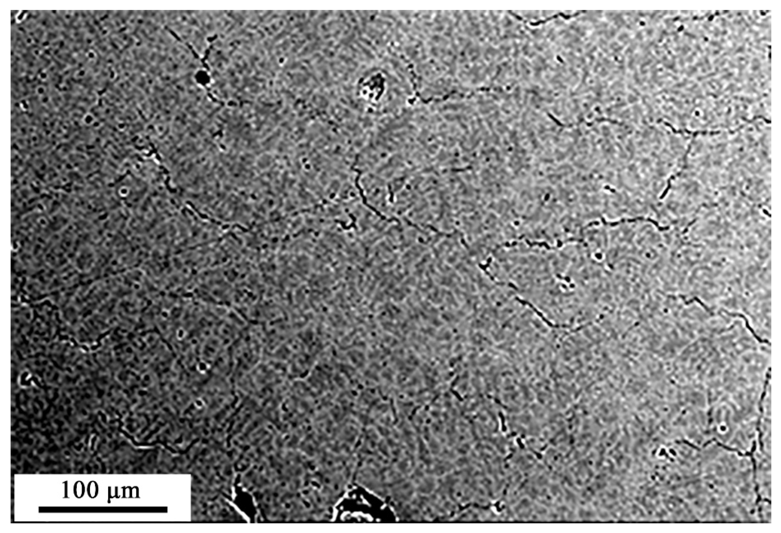
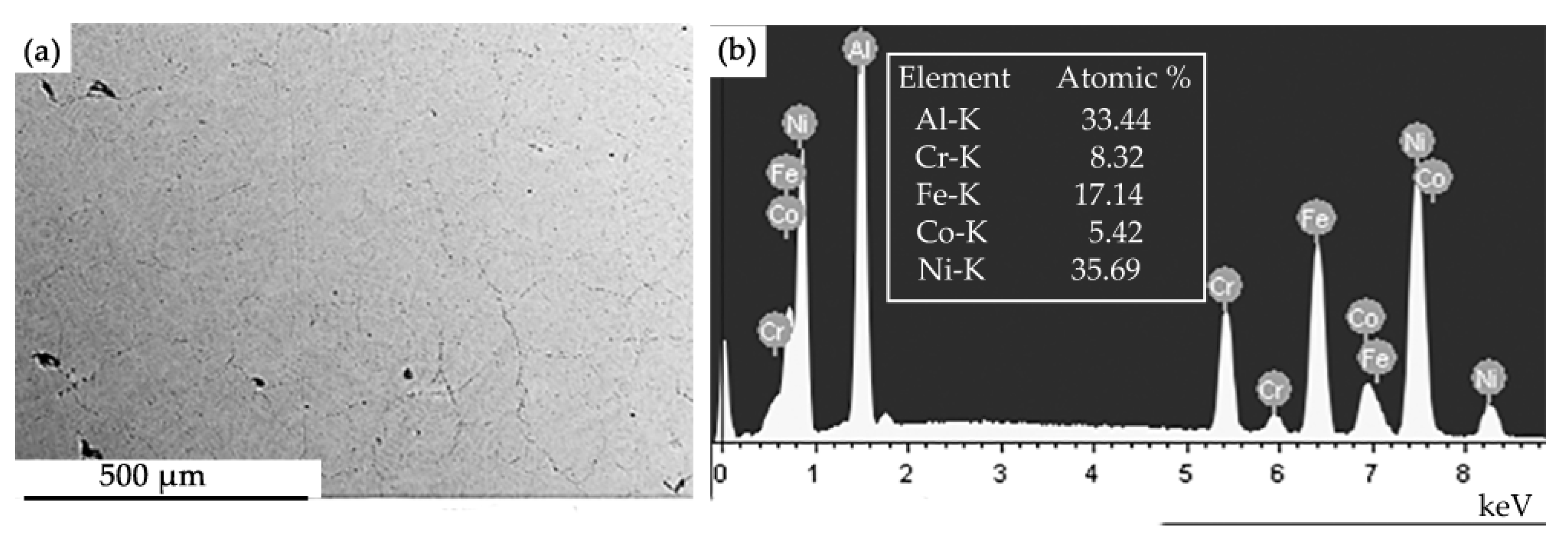
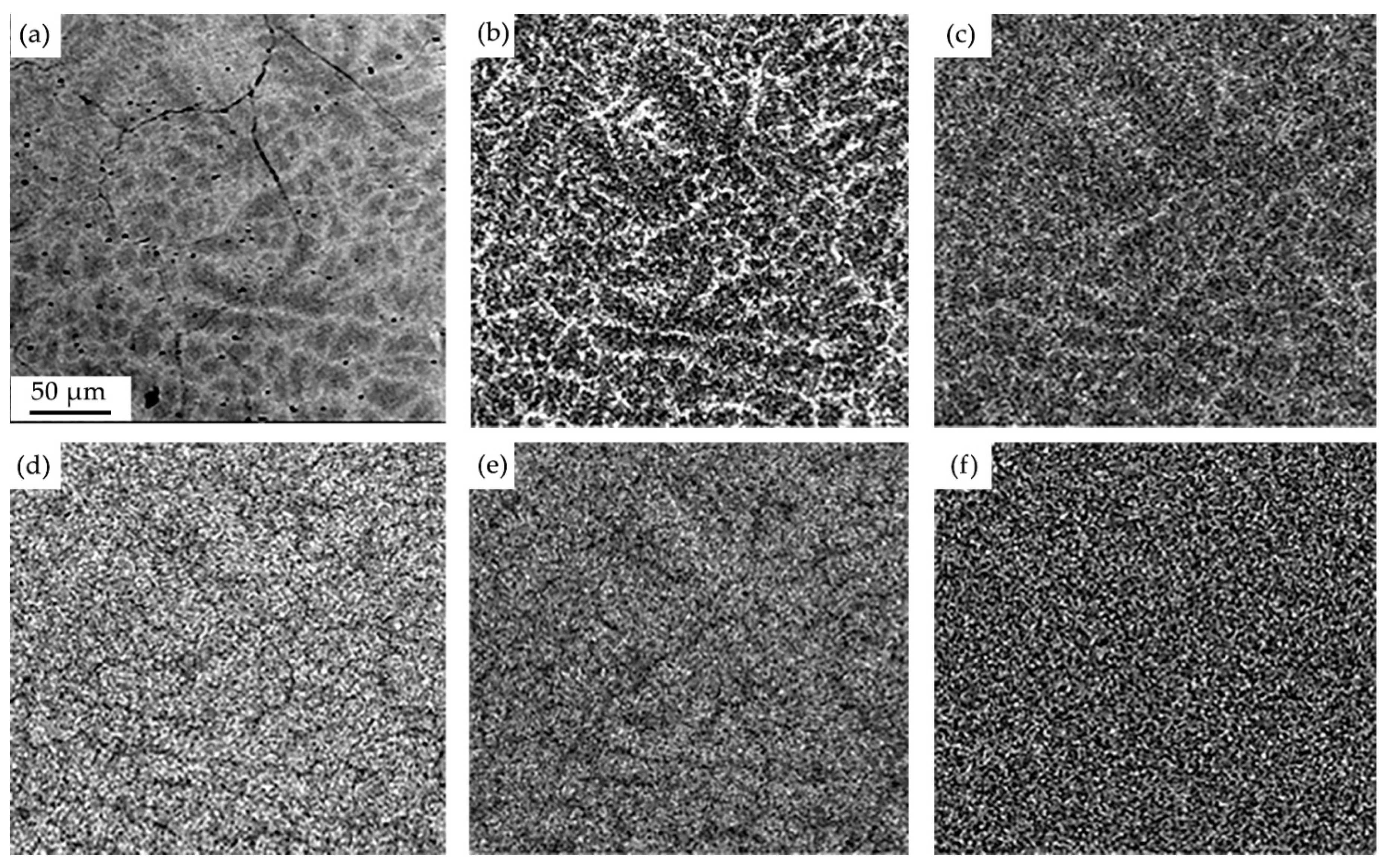
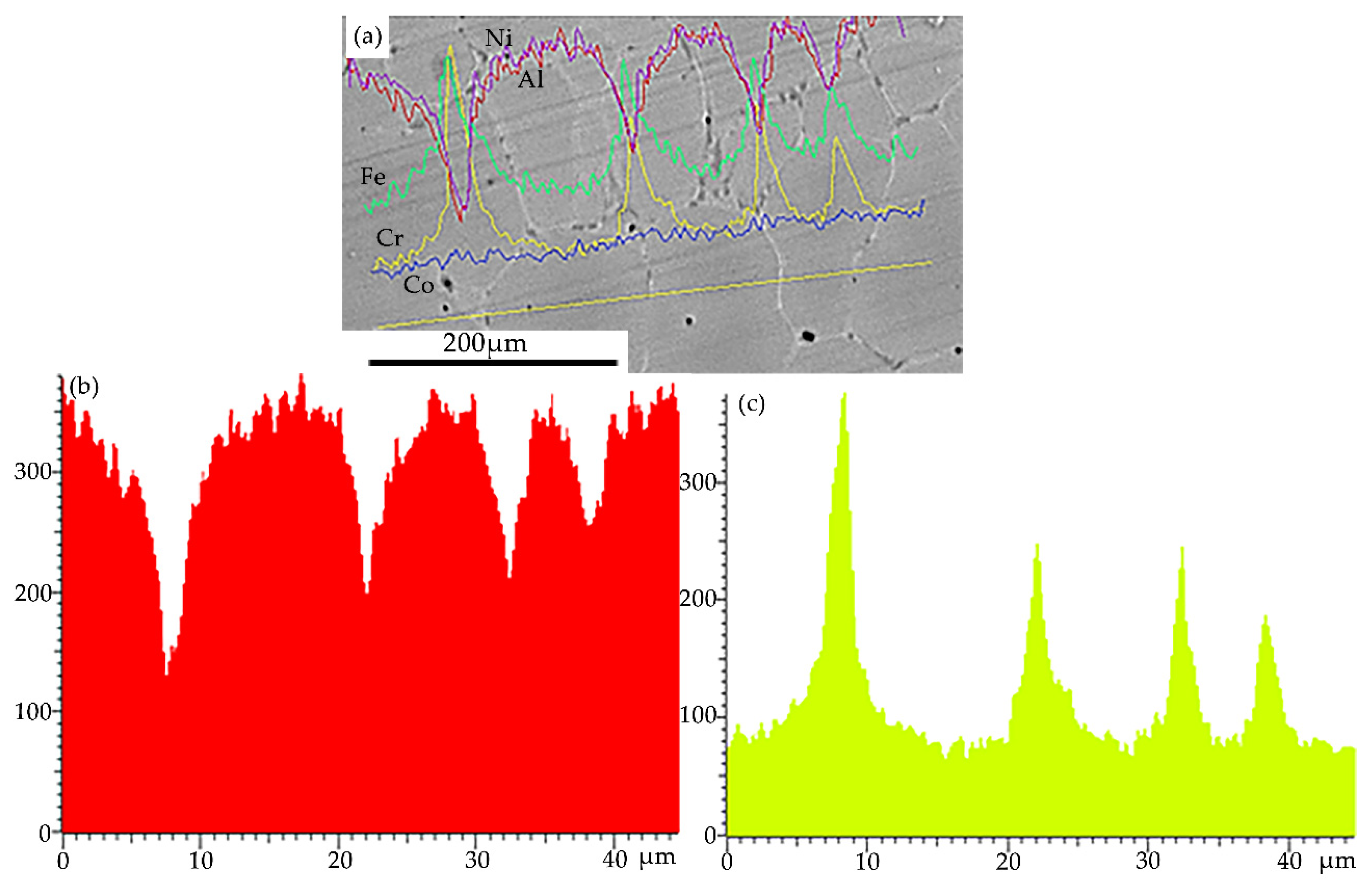
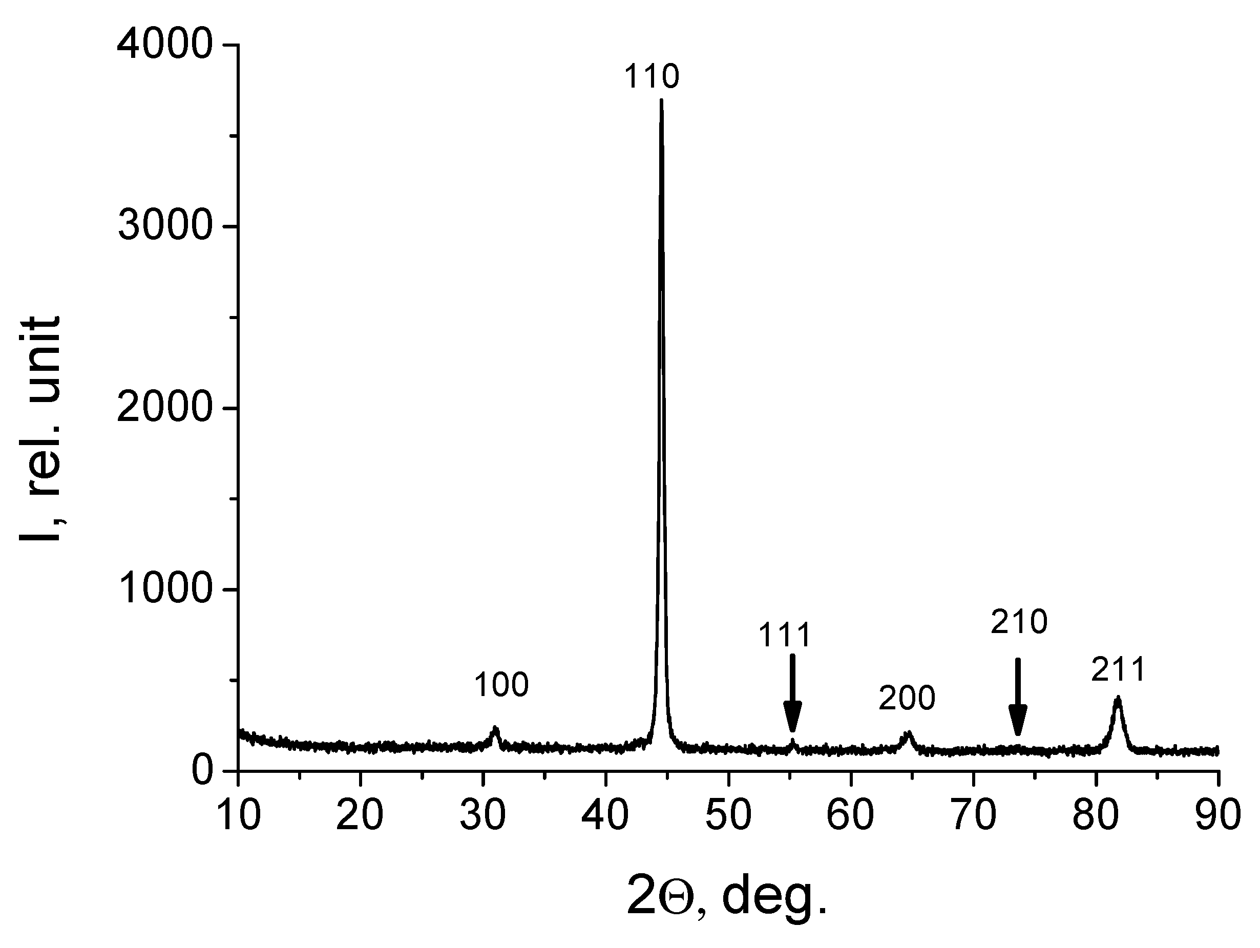
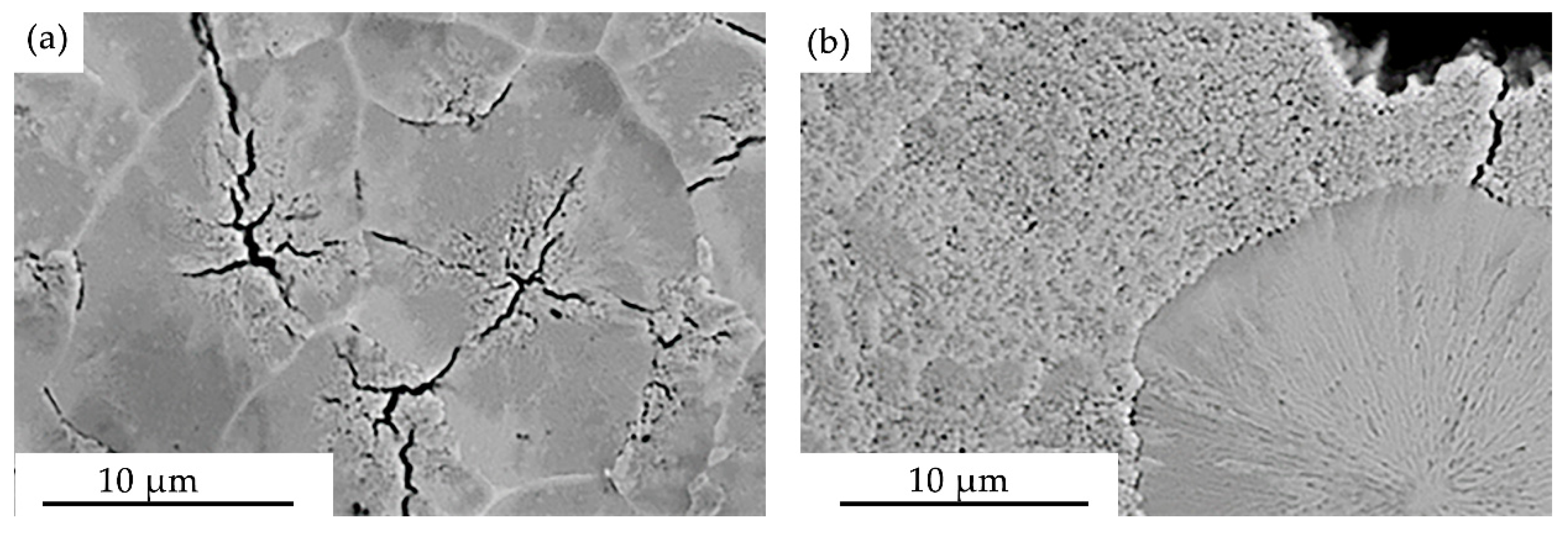
3.1. Structure and Properties of Cast HEA in the Initial State

Additive manufactured HEA has a dendritic structure (Figure 1), which is a polycrystalline aggregate with a 12.3 µm average grain size.
X-ray microanalysis showed that the HEA is formed by the chemical elements Al, Cr, Fe, Co, Ni in the following ratio (at. %): 33.4Al-8.3Cr-17.1Fe-5.4Co-35.7Ni (Figure 2). A small unindexed peak near 1.8 KeV belongs to silicon, its relative content is low (2.3 at.%). It is obvious that silicon is an uncontrolled impurity of aluminum.
The mapping method was used to visualize the distribution of atoms in the bulk of the alloy (Figure 3). It is shown that the boundaries of grains and dendrites are enriched in chromium and iron atoms; the volume of grains is enriched with aluminum, nickel, and cobalt atoms. Thus, the additive-manufactured alloy is characterized by the separation of chemical elements.
Presented in Figure 4, the results of X-ray microanalysis obtained by the “along the line” method (an example for the distribution of aluminum and chromium atoms is given) confirm the above conclusions about the quasi-periodic distribution of atoms that form the high-entropy alloy under study. Indeed, following the results shown in Figure 4, the grains are enriched with Al and Ni and can be an AlNi-based phase (Pm3m); a phase rich in chromium and iron is located within the grain boundaries, i.e., a phase based on FeCr (Im3m) BCC.
X-ray phase analysis showed that the alloy under study has a simple cubic crystal lattice (Figure 5), the crystal lattice parameter of the alloy is 0.28795 nm.
The HEA microhardness in the initial state is 4.7 GPa. The HEA wear parameter in the initial state is 14×10−5 mm3/N×m, and the friction coefficient is 0.65.

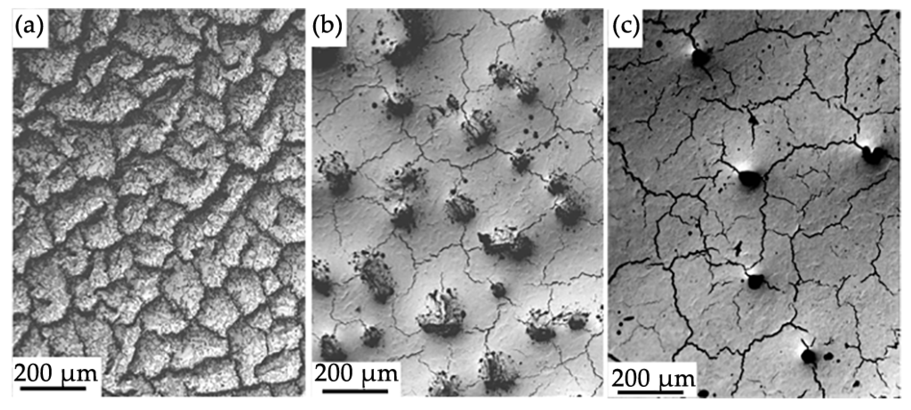
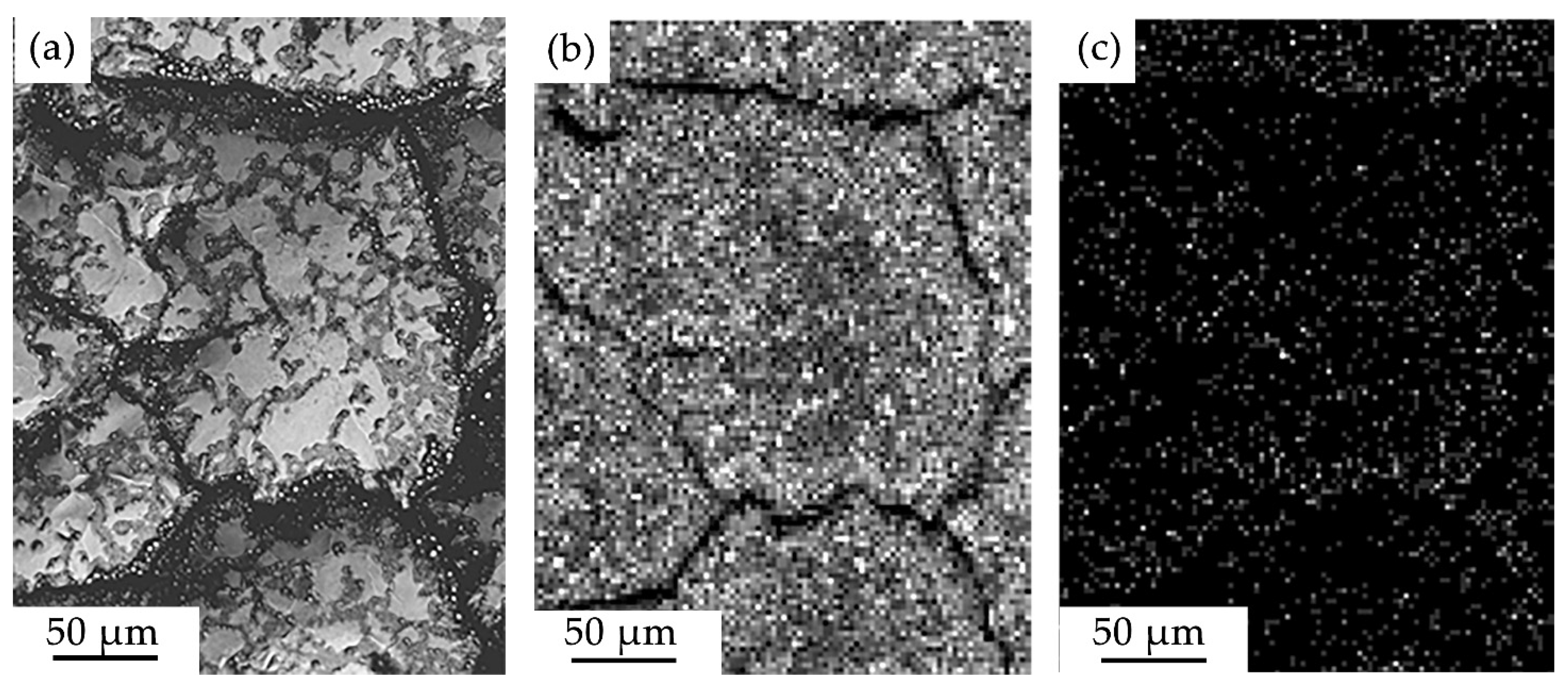
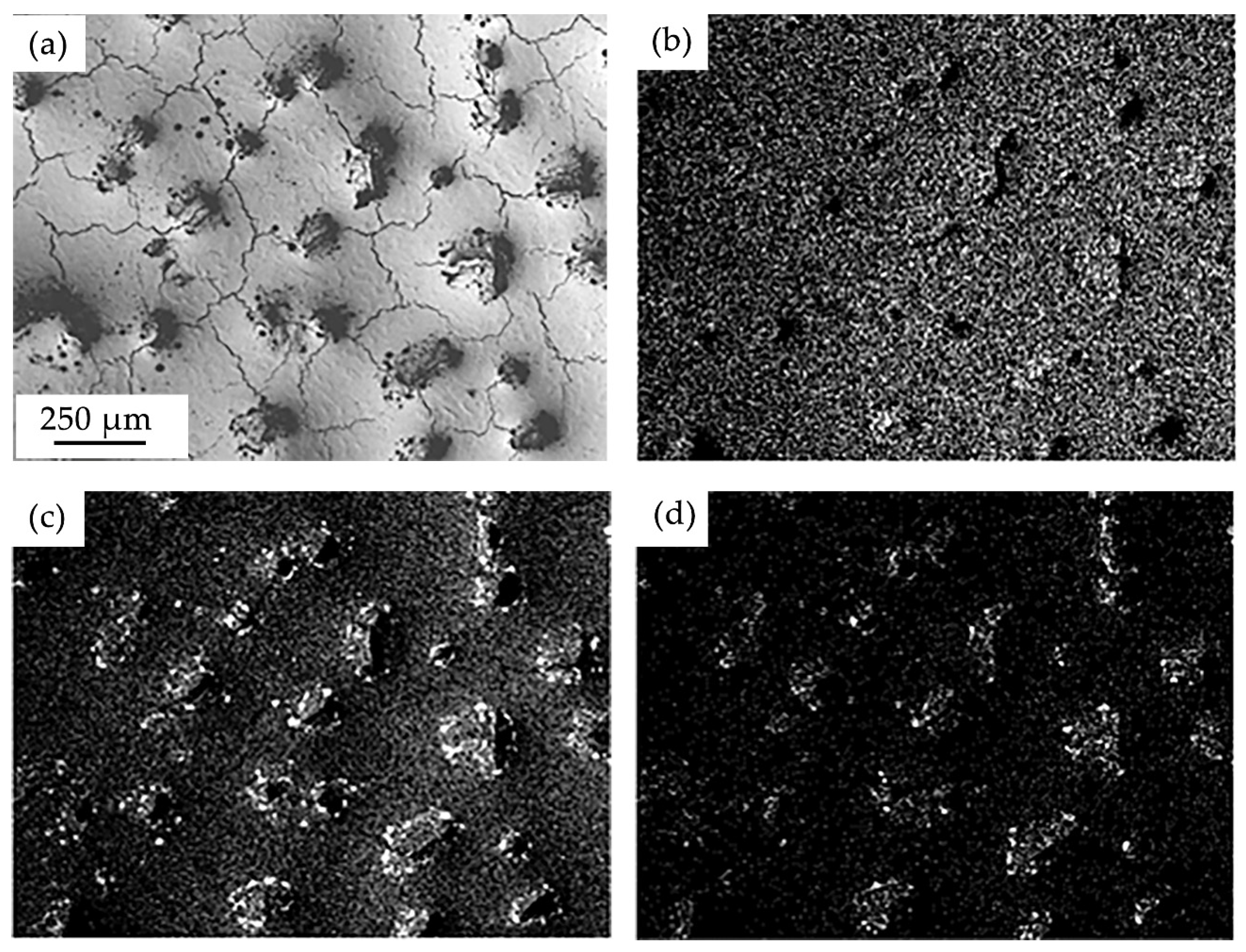
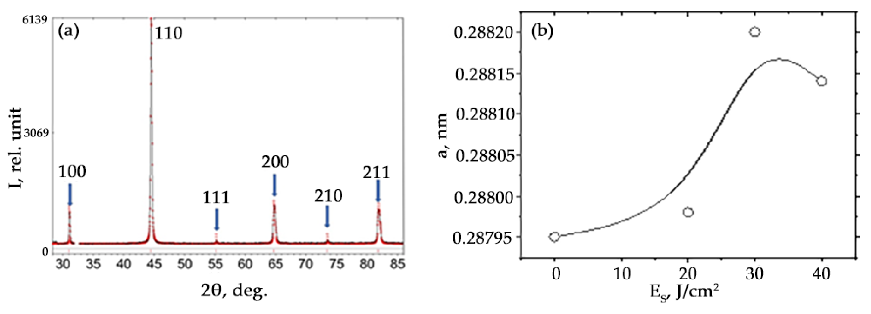
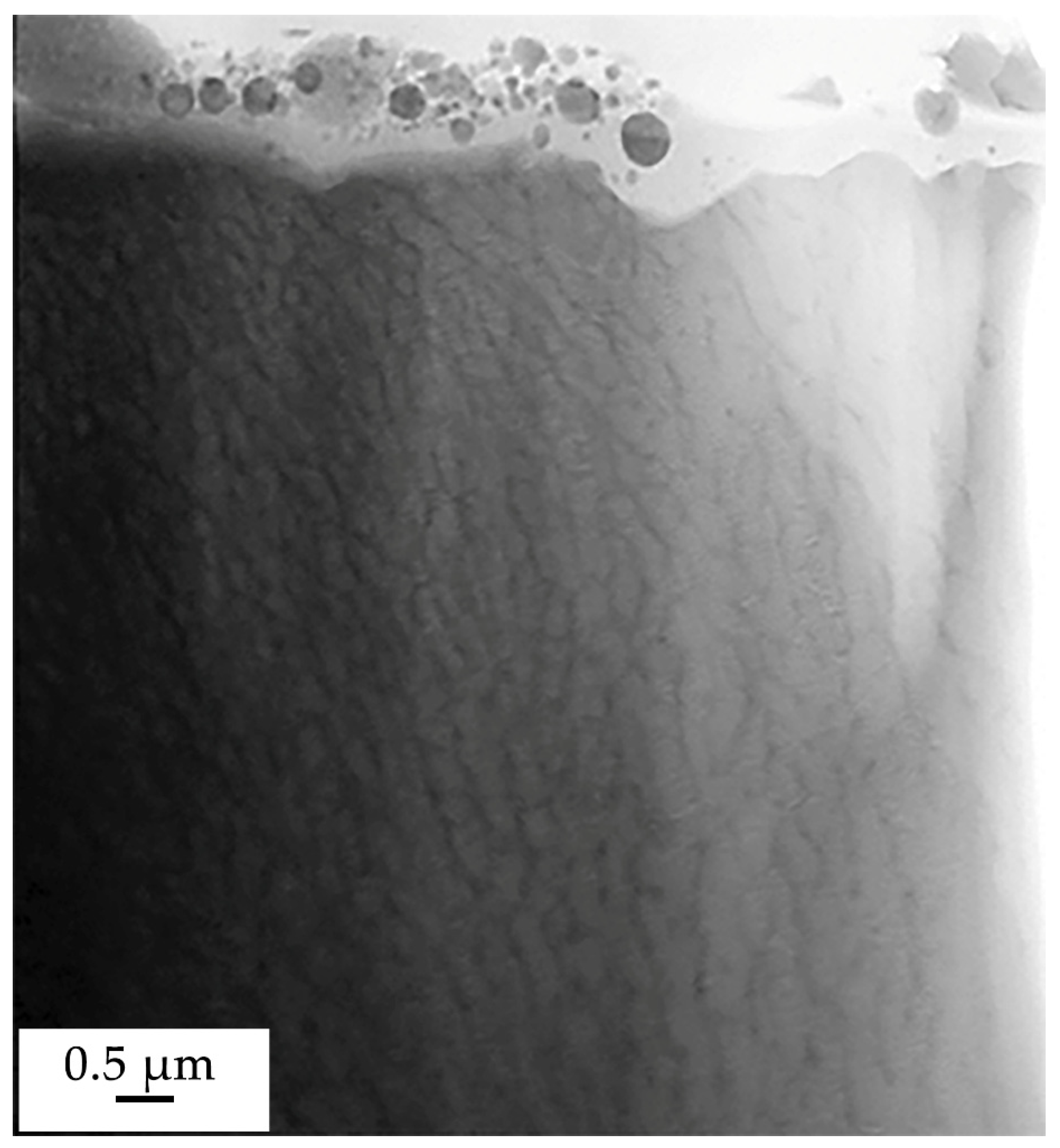
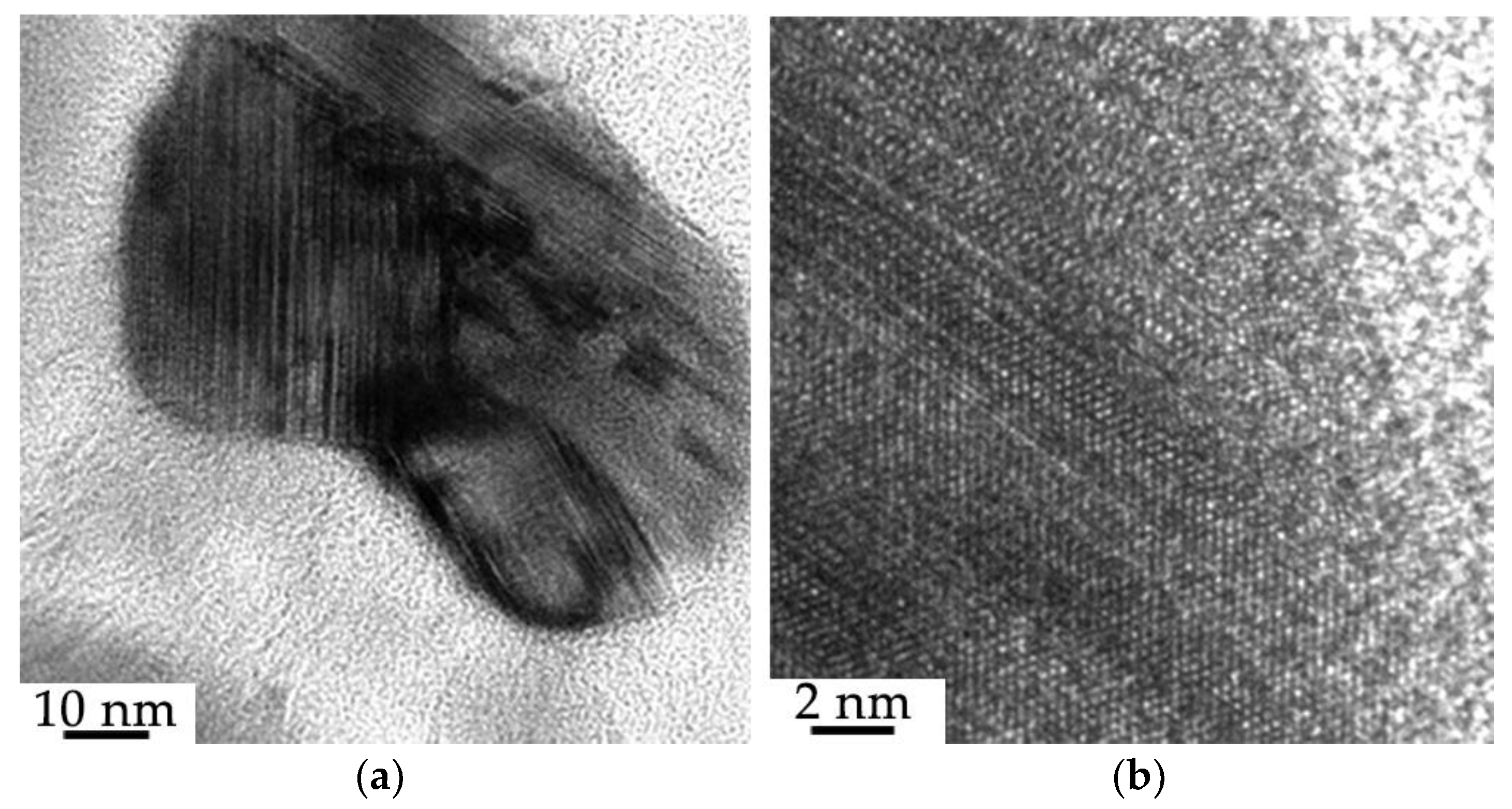
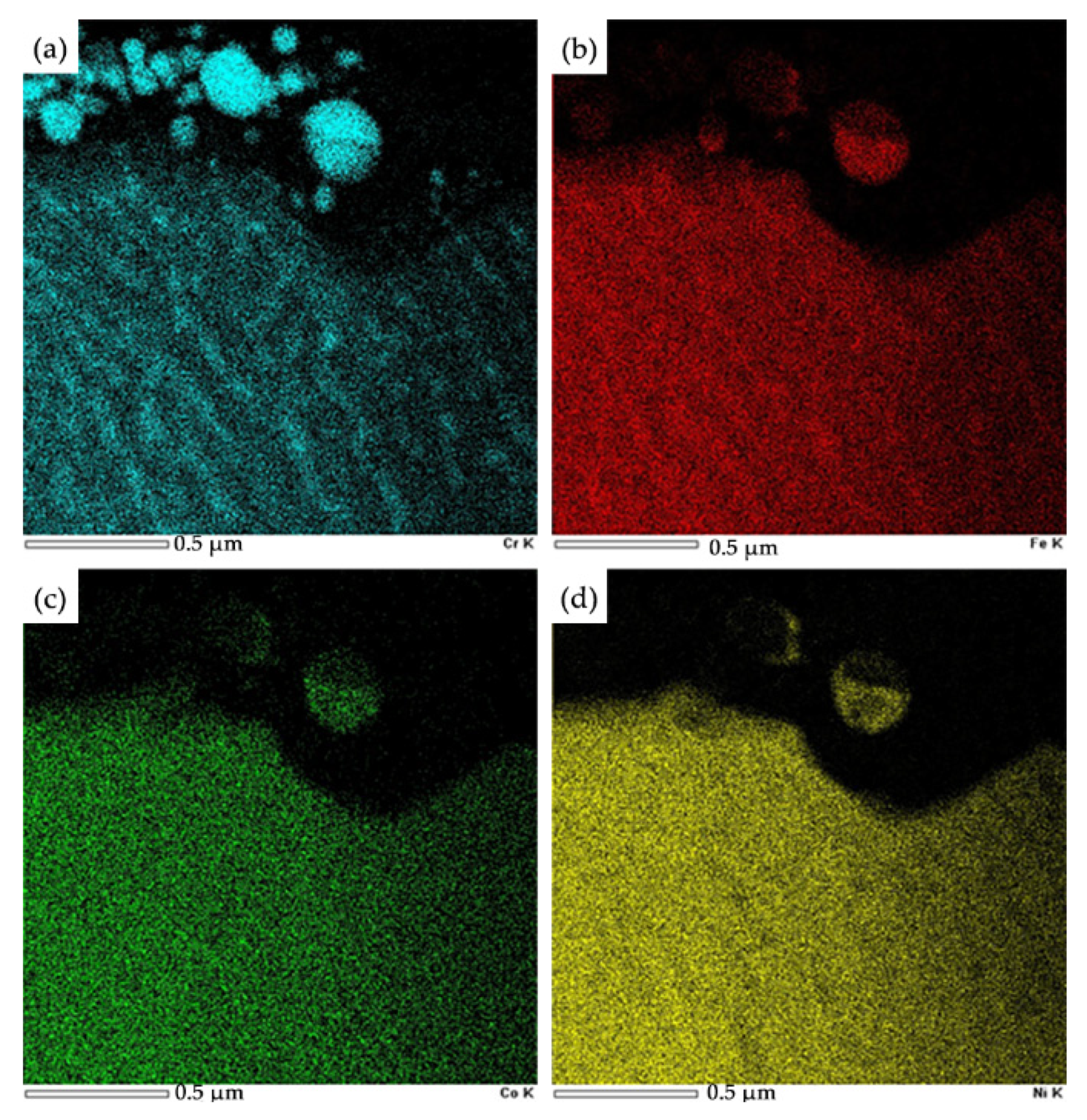
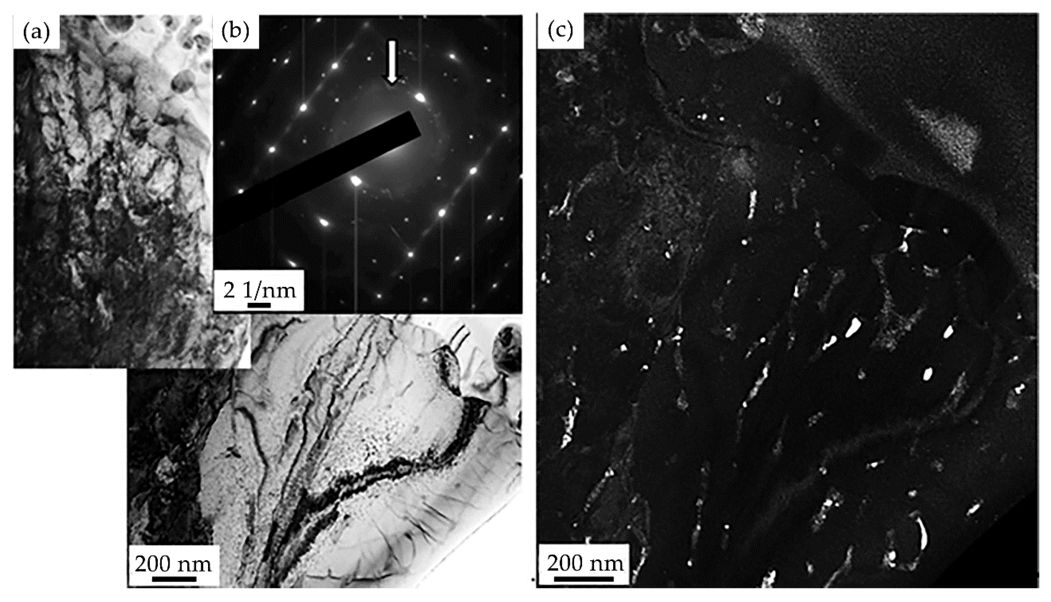
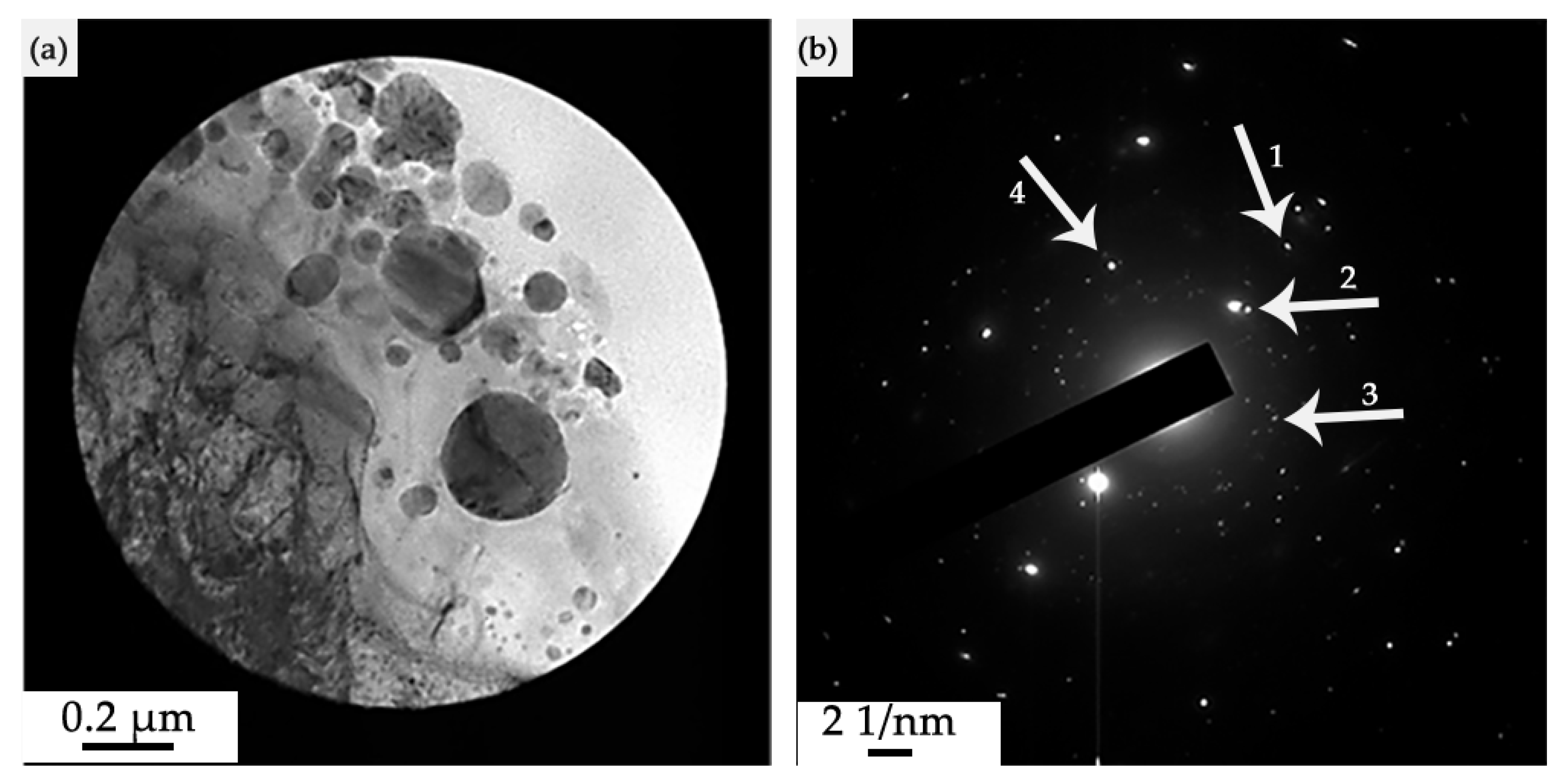
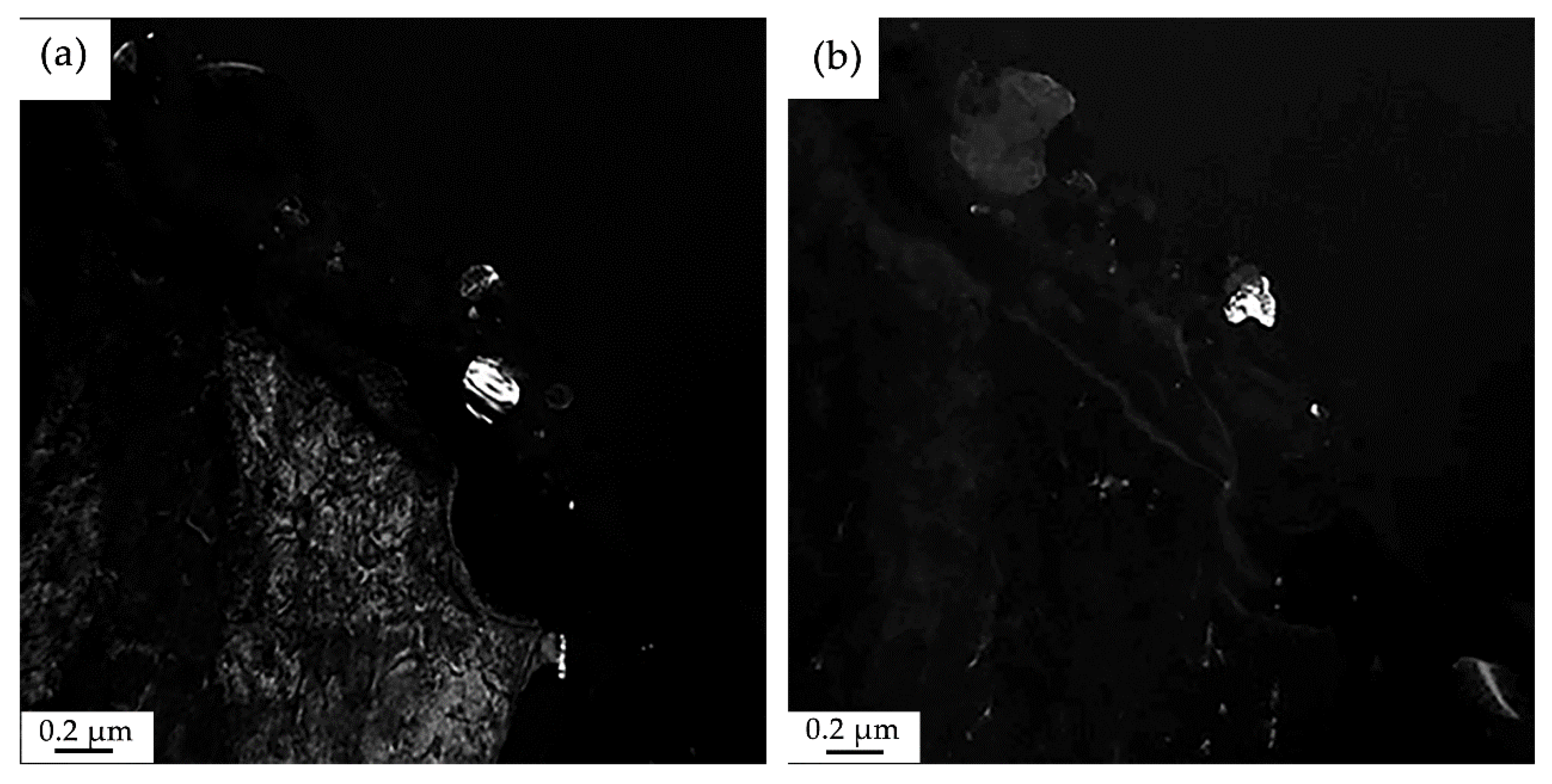
3.2. Structure and Properties of HEA Subjected to Surface Alloying and Electron Beam Processing

Irradiation of the “film (Cr + B)/(HEA) substrate” system with a pulsed electron beam with a variation in the energy density of the electron beam leads, first, to fragmentation of the surface layer with microcracks, regardless of the ES value, (Figure 6) and, second, to the formation of a “honeycomb” type structure at ES = 20 J/cm2 (Figure 7), and of island type structures at ES = (30 and 40) J/cm2, (Figure 6b,c and Figure 8). In this case, the size and number of islands per unit length decrease as the energy density of the electron beam increases (Figure 6b,c).
Using X-ray microanalysis, it was shown that when the surface of the “film (Cr + B)/(HEA) substrate” system is irradiated with a pulsed electron beam at ES = 20 J/cm2, the honeycomb boundaries are enriched predominantly with chromium and boron atoms (Figure 7). At a higher energy density of the electron beam, the formed islands are enriched with chromium, aluminum, and oxygen atoms (Figure 8). Boron atoms are not detected, which may indicate their diffusion into the volume of the surface layer of the HEA sample.
Irradiation of the “film/substrate” system by the pulsed electron beam is accompanied not only by the transformation of the film structure (Cr + B), but also by the surface layer structure of the substrates. First, a change in the grain size was revealed: if the average grain size is 12.3 µm in the original HEA samples, then after irradiation at ES = 20 J/cm2 the average grain size is 2.7 µm. The grain size increases at large values of ES, and it reaches 19.1 µm at ES = 40 J/cm2. An increase in the energy density of the electron beam leads to an increase in the cooling time of the sample and, consequently, the time of the grain growth process. Second, high-speed crystallization of the surface layer leads to the widespread formation of a subgrain structure (structure of high-speed cellular crystallization) with a crystallite size of 150–200 nm. The structure of cellular crystallization is observed at ES = 20 J/cm2 in some cases; crystallization cells are observed predominantly at grain junctions at ES = 30 J/cm2 (Figure 9a); high-speed crystallization cells cover the entire sample area at ES = 40 J/cm2 (Figure 9b).
An X-ray phase analysis of the phase composition of the HEA surface layer modified by irradiation of the “film/substrate system” with a pulsed electron beam was performed. It shows that, regardless of the electron beam energy density, the alloy is a single-phase material with a simple cubic crystal lattice (Figure 10a). At the same time, a change in the crystal lattice parameter of the alloy is detected (Figure 10b). One of the reasons for the change in the crystal lattice parameter of the alloy is the alloying of samples with boron atoms, the concentration of which in the alloy volume, judging by the results obtained by scanning electron microscopy, will increase as energy density goes up in the range ES = (20–30) J/cm2. It should be noted that the boron atoms in the HEA crystal lattice will be located at the interstitial positions, which will lead to an increase in the lattice parameter. The presence of strengthening phases in the alloy under study was not detected by X-ray phase analysis, which may be due to their small amount.
Chemical elements distribution over the thickness of the surface layer of the “film/substrate” system was studied by transmission electron microscopy of samples irradiated at ES = 20 J/cm2. The X-ray microanalysis of a foil section, the STEM image of which is given in Figure 11, showed that the main element of the examined layer is nickel (47.3 at.%); the concentration of boron atoms is 15.2 at.%. (Table 1).
The modified surface layer is characterized by the presence of formations of a spherical shape, the dimensions of which vary from units to hundreds of nanometers (Figure 11). It was established by methods of direct resolution of the crystal lattice that the particles are crystalline formations (Figure 12a); these particles are located in the layer having an amorphous structure (Figure 12b).
X-ray microanalysis proved that the particles are enriched with chromium, iron, nickel, and cobalt atoms (Figure 13). Irradiation of the “film/substrate” system is accompanied by the transformation of the HEA surface layer. A structure of high-speed crystallization of a cellular type with a cell size of (100–120) nm is formed. The cells are separated by interlayers of the second phase with a thickness of (35–45) nm. The interlayers separating the cells are enriched with chromium and iron atoms. (Figure 13a,b).
The analysis of microelectron diffraction patterns and the corresponding dark-field images made it possible to study the phase composition of the surface layer of the “film/substrate” system irradiated with a pulsed electron beam. Figure 14 provides the results of studying the phase composition of the HEA layer adjacent to the deposited film. The analysis of the microelectron diffraction pattern shows that borides of various elemental compositions are formed along the boundaries of high-speed crystallization cells. The latter indicates the saturation of the HEA surface layer with boron atoms, which occurs under conditions of short-term (hundreds of microseconds) thermal exposure. It should be noted that the thickness of the HEA layer saturated with boron will depend on the irradiation parameters (energy density of the electron beam, pulse duration, number, and repetition rate of pulses), i.e., it is a controlled quantity.
The results of electron microscopic analysis of the phase composition of the “film/substrate” system, which is formed as a result of irradiation with a pulsed electron beam (ES = 20 J/cm2), are shown in Figure 15, Figure 16 and Figure 17. A section of the foil was examined, the electron microscopic image of which, limited by the selector diaphragm, is given in Figure 15a.
As shown in Figure 16a, the dark-field image, obtained in the reflection given in Figure 15b under No. 1, indicates that the spherical particles are formed by a solid solution based on the chromium crystal lattice. Simultaneously with chromium particles, the HEA layer adjacent to the coating is illuminated in the dark-field image. Figure 16b shows a dark-field image obtained in the reflection shown in Figure 15b under No. 2. Analysis of the microelectron diffraction pattern in Figure 15b indicates that the detected particles are a phase of the composition Cr3NiB6.
The dark-field image shown in Figure 17a shows the presence of CrB and Cr2Ni3B6 particles in the surface layer; in Figure 17b—FeB particles are located in the coating and transition layer of the substrate.
Irradiation of the “film/substrate” system with a pulsed electron beam leads to a significant change in the mechanical and tribological properties of HEA samples. First, the microhardness increases significantly (almost by two times), reaching its maximum value after irradiation of the “film/substrate” system with a pulsed electron beam with an electron beam energy density of 20 J/cm2 (Figure 18).
Second, the wear resistance of the samples increases (by more than 5 times), and the friction coefficient decreases (by 1.3 times), reaching the best values after irradiation of the “film/substrate” system with a pulsed electron beam with an electron beam energy density of 20 J/cm2 (Figure 19).
The studies of the elemental and phase composition and the state of the defect substructure carried out in this work allow us to conclude that the main physical mechanisms for increasing the mechanical and tribological properties of the modified HEA layer are, first, grain boundary, due to the decrease in the average grain size of the alloy during irradiation and the formation of a cellular crystallization structure, second, the solid solution, due to the incorporation of boron atoms into the HEA crystal lattice, third, dispersion, due to the formation of nanosized particles of the second phase in the volume and at the boundaries of grains and cells.

4. Conclusions

HEA samples of non-equiatomic elemental composition AlCrFeCoNi were fabricated by WAAM. A complex processing of the HEA samples surface layer was carried out, combining the formation of the “film (Cr + B)/(HEA) substrate” system and subsequent irradiation with a pulsed electron beam at various (20–40 J/cm2) values of the electron beam energy density. The irradiation mode (20 J/cm2, 200 µs, 3 pulses, 0.3 s−1) was revealed, which makes it possible to significantly increase the microhardness (almost by 2 times) and wear resistance (more than 5 times), reduce the friction coefficient by 1.3 times. As a result of the performed studies of the structure and phase composition, it was suggested that improvement in the strength and tribological properties of HEA is due to a significant (4.5 times) decrease in the average grain size, the formation of particles of chromium and aluminum oxyborides, and the incorporation of boron atoms into the crystal lattice of HEA.

Author Contributions

Conceptualization, V.G., Y.I., I.P. and S.K.; methodology, S.K. and Y.I.; software, Y.I. and V.G.; validation, Y.I., M.E., A.T., E.P., I.P. and Y.S.; formal analysis, V.S., M.E., A.T., E.P., I.P. and Y.S.; investigation, Y.I., V.G., S.K., V.S., M.E., A.T., E.P., I.P. and Y.S.; resources, Y.I. and V.G.; data curation, V.S., M.E., A.T. and E.P.; writing—original draft preparation, M.E., A.T. and E.P.; writing—review and editing, S.K., I.P. and Y.S.; visualization, S.K., V.S. and M.E.; supervision, Y.I. and V.G.; project administration, S.K. and Y.I.; funding acquisition, Y.I. and V.G. All authors have read and agreed to the published version of the manuscript.

Funding

The work was supported by a grant of the Russian Science Foundation No. 19-19-00183, https://rscf.ru/project/19-19-00183/–HEA (accessed on 10 September 2022) modification, study of the structure and properties of the modified HEA layer; by the grant of the Russian Science Foundation (project No. 20-19-00452)—fabrication of HEA samples using cold metal transfer technology.

Data Availability Statement

Not applicable.

Conflicts of Interest

The authors declare no conflict of interest.

References

  1. Gromov, V.E.; Konovalov, S.V.; Ivanov, Y.F.; Osintsev, K.A. Structure and Properties of High Entropy Alloys; Springer International Publishing: Cham, Switzerland, 2021; 110p. [Google Scholar]
  2. Rogachev, A.S. Structure, stability and properties of HEA. Phys. Met. Met. Sci. 2020, 121, 807–841. [Google Scholar] [CrossRef]
  3. Yeh, J.-W.; Chen, S.-K.; Lin, S.-J.; Gan, J.-Y.; Chin, T.-S.; Shun, T.-T.; Tsau, C.-H.; Chang, S.-Y. Nanostructured high-entropy alloys with multiple principal elements: Novel alloy design concepts and outcomes. Adv. Eng. Mater. 2004, 6, 299–303. [Google Scholar] [CrossRef]
  4. Zhang, Y.; Zuo, T.T.; Tang, Z.; Gao, M.C.; Dahmen, K.A.; Liaw, P.K.; Lu, Z.P. Microstructures and properties of high-entropy alloys. Prog. Mater. Sci. 2014, 61, 1–93. [Google Scholar] [CrossRef]
  5. Cantor, B. Multicomponent and high entropy alloys. Entropy 2014, 16, 4749–4768. [Google Scholar] [CrossRef] [Green Version]
  6. Miracle, D.B.; Senkov, O.N. A critical review of high entropy alloys and related concepts. Acta Mater. 2017, 122, 448–511. [Google Scholar] [CrossRef] [Green Version]
  7. Zhang, W.; Liaw, P.K.; Zhang, Y. Science and technology in high-entropy alloys. Sci China Mater. 2018, 61, 2–22. [Google Scholar] [CrossRef] [Green Version]
  8. Gorban, V.F.; Krapivka, N.A.; Firstov, S.A. High-entropy alloys: Interrelations between electron concentration, phase composition, lattice parameter, and properties. Phys. Metals Metallogr. 2017, 118, 970–981. [Google Scholar] [CrossRef]
  9. Yeh, J.-W.; Chen, S.-K.; Gan, J.-Y.; Lin, S.-J.; Chin, T.-S.; Shun, T.-T.; Tsau, C.-H.; Chang, S.-Y. Formation of simple crystal structures in Cu-Co-Ni-Cr-Al-Fe-Ti-V alloys with multiprincipal metallic elements. Metal. Mater. Trans. A 2004, 35A, 2533–2536. [Google Scholar] [CrossRef]
  10. Yeh, J.-W. Recent progress in high-entropy alloys. Ann. Chim. Sci. Mater. 2006, 31, 633–648. [Google Scholar] [CrossRef]
  11. Tong, C.J.; Chen, S.K.; Yeh, J.W.; Shun, T.T.; Tsau, C.H.; Lin, S.J.; Chang, S.Y. Microstructure Characterization of AlxCoCrCuFeNi High-Entropy Alloy System with Multi-principal Elements. Metall. Mater. Trans. A 2004, 36A, 881–893. [Google Scholar]
  12. Tsai, K.-Y.; Tsai, M.-H.; Yeh, J.-W. Sluggish diffusion in Co–Cr–Fe–Mn–Ni high-entropy alloys. Acta Mater. 2013, 61, 4887–4897. [Google Scholar] [CrossRef]
  13. Tsai, M.-H.; Yeh, J.-W. High-entropy alloys: A critical review. Mater. Res. Lett. 2014, 2, 107–123. [Google Scholar] [CrossRef]
  14. Alaneme, K.K.; Bodunrin, M.O.; Oke, S.R. Processing, alloy composition and phase transition effect on the mechanical and corrosion properties of high entropy alloys: A review. J. Mater. Res. Technol. 2016, 5, 384–393. [Google Scholar] [CrossRef] [Green Version]
  15. Murty, B.S.; Yeh, J.W.; Ranganathan, S.; Bhattacharjee, P.P. High-Entropy Alloys, 2nd ed.; Elsevier: Amsterdam, The Netherlands, 2019; 374p. [Google Scholar]
  16. Zhang, Y. High-Entropy Materials. A Brief Introduction; Springer Nature: Singapore, 2019; 159p. [Google Scholar]
  17. Ma, Y.; Peng, G.J.; Ven, D.H.; Zhang, T.H. Nanoindentation creep behavior in a CoCrFeCuNi high-entropy alloys film with two different structure states. Mater. Sci. Eng. A 2015, 621, 111–117. [Google Scholar] [CrossRef]
  18. Wang, L.M.; Chen, G.G.; Yeh, J.W.; Ke, S.T. The microstructure and strengthening mechanism of thermal spray coating NixCo0.6 Fe0.2CrySizAlTi0.2 high-entropy alloys. Mater. Chem. Phy. 2011, 126, 880–885. [Google Scholar] [CrossRef]
  19. Zhang, H.; Wu, W.; He, Y.; Li, M.X.; Guo, S. Formation of core-shell structure in high-entropy alloy coating by laser cladding. Appl. Surf. Sci. 2015, 363, 543–547. [Google Scholar] [CrossRef]
  20. Gao, W.Y.; Chang, C.; Li, G.; Xue, Y.F.; Wang, J.J.; Zhang, Z.Y.; Lin, X.G. Study on the laser cladding of FeCrNi coating. Optik 2019, 178, 950–957. [Google Scholar] [CrossRef]
  21. Rong, Z.; Wang, C.; Wang, Y.; Dongetal, M. Microstructure and properties of FeCoNiCrX (Xdouble bondMn, Al) high-entropy alloy coatings. J. Alloy. Compd. 2022, 921, 166061. [Google Scholar] [CrossRef]
  22. Chang, S.Y.; Lin, S.Y.; Huang, Y.C.; Wu, C.L. Mechanical properties, deformation behaviors and interface adhesion of (AlCrTaTiZr)Nx multi-component coatings. Surf. Coat. Technol. 2010, 204, 3307–3314. [Google Scholar] [CrossRef]
  23. Shen, W.-J.; Tsai, M.-H.; Chang, Y.-S.; Yeh, J.-W. Effects of substrate bias on the structure and mechanical properties of (Al1.5CrNb0.5Si0.5Ti)Nx coatings. Thin Solid Film. 2012, 520, 6183–6188. [Google Scholar] [CrossRef]
  24. Braic, V.; Vladescu, A.; Balaceanu, M.; Luculescu, C.R.; Braic, M. Nanostructured multi-element (TiZrNbHfTa)N and (TiZrNbHfTa)C hard coatings. Surf. Coat. Technol. 2012, 211, 117–121. [Google Scholar] [CrossRef]
  25. Lin, M.I.; Tsai, M.H.; Shen, W.J.; Yeh, J.W. Evolution of structure and properties of multi-component (AlCrTaTiZr)Ox films. Thin Solid Films. 2010, 518, 2732–2737. [Google Scholar] [CrossRef]
  26. Zhao, Y.; Zhang, J.; Wang, Y.; Wu, K.; Liu, G.; Sun, J. Size- dependent mechanical properties and deformation mechanisms in Cu/NbMoTaW nanolaminates. Sci. China Mater. 2020, 63, 444–452. [Google Scholar] [CrossRef] [Green Version]
  27. Cao, Z.H.; Ma, Y.J.; Cai, Y.P.; Wang, G.J.; Meng, X.K. High strength dual-phase high entropy alloys with a tunable nanolayer thickness. Scr. Mater. 2019, 173, 149–153. [Google Scholar] [CrossRef]
  28. Xu, H.; Zang, J.; Yuan, Y.; Zhou, Y.; Tian, P.; Wang, Y. In-situ assembly from graphene encapsulated CoCrFeMnNi high-entropy alloy nanoparticles for improvement corrosion resistance and mechanical properties in metal matrix composites. J. Alloys Compd. 2019, 811, 152082. [Google Scholar] [CrossRef]
  29. Wang, Y.; Kuang, S.; Yu, X.; Wang, L.; Huang, W. Tribo-mechanical properties of CrNbTiMoZr high-entropy alloy film synthesized by direct current magnetron sputtering. Surf. Coat. Technol. 2020, 403, 126374. [Google Scholar] [CrossRef]
  30. Zhoo, S.; He, L.; Fan, X.; Liu, C.; Long, J.; Wang, L.; Chang, H.; Wang, J.; Zhang, W. Microstructure and chloride corrosion property of nanocrystalline AlTiCrNiTa high entropy alloy coating on X80 pipeline steel. Surf. Coat. Technol. 2019, 375, 215–220. [Google Scholar] [CrossRef]
  31. Wu, H.; Zhang, S.; Wang, Z.Y.; Zhang, C.H.; Chen, H.T.; Chen, J. New studies on wear and corrosion behavior of laser cladding FeNiCoCrMox high entropy alloy coating: The role of Mo. Inter. J. Refectory Met. Hard Mater. 2022, 102, 105721. [Google Scholar] [CrossRef]
  32. Ye, F.; Jiao, Z.; Gio, L.; Feng, L.; Yu, J. Microbeam plasma arc remanufacturing: Effects of Al on microstructure, wear resistance, corrosion resistance and high temperature oxidation resistance of AlxCoCrFeMnNi high-entropy alloy cladding layer. Vacuum 2020, 174, 109178. [Google Scholar] [CrossRef]
  33. Zhang, G.; Liu, H.; Tian, X.; Chen, P.; Yang, H.; Hao, J. Microstructure and properties of AlCoCrFeNiSi high-entropy alloy coating on AISI 304 stainless steel by laser cladding. J. Mater. Eng. Perform. 2020, 29, 278–288. [Google Scholar] [CrossRef]
  34. Liu, H.; Zhang, T.; Sum, S.; Zhang, G.; Tian, X.; Chen, P. Microstructure and dislocation density of AlCoCrFeNiSix high entropy alloy coatings by laser cladding. Mater. Lett. 2021, 283, 128746. [Google Scholar] [CrossRef]
  35. Ye, Q.; Feng, K.; Li, Z.; Lu, F.; Li, R.; Huang, J.; Wu, Y. Microstructure and corrosion properties of CrMnFeCoNi high entropy alloy coating. Appl. Surf. Sci. 2017, 396, 1420–1426. [Google Scholar] [CrossRef]
  36. Jiang, H.; Han, K.; Li, D.; Cao, Z. Synthesis and characterization of AlCoCrFeNiNbx high-entropy alloy coatings by laser cladding. Crystals 2019, 9, 56. [Google Scholar] [CrossRef] [Green Version]
  37. Liu, S.S.; Zhang, M.; Zhao, G.L.; Wang, X.H.; Wang, J.F. Microstructure and properties of ceramic particle reinforced FeCoNiCrMnTi high entropy alloy laser cladding coating. Intermetallics 2022, 140, 107402. [Google Scholar] [CrossRef]
  38. Zhong, M.; Wang, D.; He, L.; Ye, X.; Ouyang, W.; Xu, Z.; Zhang, W.; Zhou, X. Microstructure and elevated temperature wear behavior of laser-cladded AlCrFeMnNi high-entropy alloy coating. Opt. Laser Technol. 2022, 149, 107845. [Google Scholar] [CrossRef]
  39. Zhang, P.; Xu, Z.; Yao, Z.; Liu, Y.; Lin, S.; He, M.; Lu, S.; Wu, X. A high-corrosion-resistant high-entropy alloys (HEAs) coatings with single BCC solid solution structure by laser remelting. Mater. Lett. 2022, 324, 132728. [Google Scholar] [CrossRef]
  40. Liu, H.; Li, X.; Liu, J.; Gao, W.; Du, X.; Hao, J. Microstructural evolution and properties of dual-layer CoCrFeMnTi0.2 high-entropy alloy coating fabricated by laser cladding. Opt. Laser Technol. 2021, 134, 106646. [Google Scholar] [CrossRef]
  41. Jiang, X.J.; Wang, S.Z.; Fu, H.; Chen, G.Y.; Ran, Q.X.; Wang, S.Q.; Han, R.H. A novel high-entropy alloy coating on Ti-6Al-4V substrate by laser cladding. Mater. Lett. 2022, 308, 131131. [Google Scholar] [CrossRef]
  42. Deng, C.; Wang, C.; Chai, L.; Wang, T.; Luo, J. Mechanical and chemical properties of CoCrFeNiMo0,2 HEA coating fabricated on Ti-6Al-4V by laser cladding. Intermetallics 2022, 144, 107504. [Google Scholar] [CrossRef]
  43. Bingyan, H.; Shayoi, B.; Wenbo, D.; Weihing, H.; Xue, Y.; Fangfang, C.; Jiajie, C.; Xianghan, G.; Sheng, Z. Laser-irradiation-induced dynamically recrystallized microstructure and properties of supersonic-particle-deposited Ni-Fe-Cr-Nb-Ti-Al high-entropy alloy coating. Mater. Charact. 2022, 183, 111600. [Google Scholar] [CrossRef]
  44. Guo, J.; Goh, M.; Zhu, Z.; Lee, X.; Nai, M.L.S.; Wei, J. On the machining of selective laser melting CoCrFeMnNi high-entropy alloy. Mater. Des. 2018, 153, 211–220. [Google Scholar] [CrossRef]
  45. Lindner, T.; Lobel, M.; Sattler, B.; Lampke, T. Surface hardening of FCC phase high-entropy alloy system by powder-pack boriding. Surf. Coat. Technol. 2019, 37, 389–394. [Google Scholar] [CrossRef]
  46. Erdogan, A.; Giinen, A.; Gok, M.S.; Zeytin, S. Microstructure and mechanical properties of borided CoCrFeNiAl0.25Ti0.5 high entropy alloy produced by powder metallurgy. Vacuum 2021, 183, 109820. [Google Scholar] [CrossRef]
  47. Ivanov, Y.F.; Gromov, V.E.; Zagulyaev, D.V.; Konovalov, S.V.; Rubannikova, Y.A.; Semin, A.P. Prospects for the application of surface treatment of alloys by electron beams in state of the art technologies. Prog. Phys. Met. 2020, 21, 345–362. [Google Scholar] [CrossRef]
  48. Gromov, V.E.; Konovalov, S.V.; Ivanov, Y.F.; Shliarova, Y.A.; Vorobyov, S.V.; Semin, A.P. Structure and properties of the CrMnFeCoNi high-entropy alloy irradiated with a pulsed electron beam. J. Mater. Res. Techn. 2022, 19, 4258–4269. [Google Scholar] [CrossRef]
  49. Osintsev, K.A.; Gromov, V.E.; Ivanov, Y.F.; Konovalov, S.V. Evolution of structure in AlCoCrFeNi HEA irradiated by pulsed electron beam. Metals 2021, 11, 1228. [Google Scholar] [CrossRef]
  50. Nevskii, S.A.; Konovalov, S.V.; Osintsev, K.A.; Ivanov, Y.F.; Granovskii, A.Y.; Gromov, V.E. The mechanism of formation of surface micro- and nanostructures in the AlCoCrFeNi high-entropy alloy during electron-beam treatment. Lett. Mater. 2021, 11, 309–314. [Google Scholar] [CrossRef]
Figure 1. Structure of the additive manufactured HEA.
Metals 12 01987 g001
Figure 2. Electron microscopic image of the HEA structure (a); (b)—energy spectra of the HEA section shown in (a).
Metals 12 01987 g002
Figure 3. Electron microscopic image of the HEA structure (a); (bf)—images of a sample section (a), obtained in the characteristic X-ray radiation of Cr (b), Fe (c), Ni (d), Al (e), Co (f) atoms.
Metals 12 01987 g003
Figure 4. Results of X-ray microspectral analysis of HEA sample section (a), obtained by the “along the line” method (blue line: Co; yellow line: Cr; green line: Fe; red line: Al; purple line: Ni); (b,c)—distribution of the intensities of characteristic X-ray emission of Al (b) and Cr (c) atoms along the line indicated in (a).
Metals 12 01987 g004
Figure 5. Fragment of the HEA X-ray diffraction pattern before modification (arrows indicate indices).
Metals 12 01987 g005
Figure 6. Electron microscopic image of the surface structure of the “film (Cr + B)/(HEA) substrate” system irradiated with a pulsed electron beam at electron beam energy density (J/cm2) of 20 (a), 30 (b), 40 (c).
Metals 12 01987 g006
Figure 7. Electron microscopic image of the surface structure of the “film (Cr + B)/(HEA) substrate” system irradiated with a pulsed electron beam (20 J/cm2) (a); (b,c)—images of the sample area (a) obtained in the characteristic X-ray emission of Cr (b) and B (c) atoms.
Metals 12 01987 g007
Figure 8. Electron microscopic image of the surface structure of the “film (Cr + B)/(HEA) substrate” system irradiated with a pulsed electron beam (30 J/cm2) (a); (bd)—images of the sample area (a), obtained in the characteristic X-ray emission of Cr (b), Al (c) and O (d) atoms.
Metals 12 01987 g008
Figure 9. Electron microscopic image of the surface structure of the “film (Cr + B)/(HEA) substrate” system irradiated with a pulsed electron beam at electron beam energy density (J/cm2) of 30 (a) and 40 (b).
Metals 12 01987 g009
Figure 10. Fragment of the X-ray diffraction pattern of HEA surface layer modified by irradiating the “film/substrate” system with a pulsed electron beam at ES = 30 J/cm2 (arrows indicate indices) (a); (b)—dependence of the HEA lattice parameter on the energy density of the electron beam.
Metals 12 01987 g010
Figure 11. Electron microscopic image (STEM analysis method) of a foil section.
Metals 12 01987 g011
Figure 12. Structure of the surface layer of the “film (B + Cr)/(HEA) substrate” system irradiated with a pulsed electron beam (ES = 20 J/cm2); (a) crystalline structure of particles; (b) amorphous structure of the layer.
Metals 12 01987 g012
Figure 13. Image of the surface layer structure of the “film/substrate” system irradiated with a pulsed electron beam (ES = 20 J/cm2), obtained in the characteristic X-ray radiation of chromium, iron, cobalt, nickel atoms. (a)—Cr; (b)—Fe; (c)—Co; (d)—Ni.
Metals 12 01987 g013
Figure 14. Electron microscopic image of the structure of HEA surface layer formed as a result of irradiation of the “film/substrate” system with a pulsed electron beam (ES = 20 J/cm2); (a)—bright-field image; (b)—microelectron diffraction pattern obtained from this section of the foil; (c)—dark-field image obtained in [111]CrB + [131]Cr3NiB6 reflections. In (b), the arrow indicates the reflection in which the dark-field image was obtained (c).
Metals 12 01987 g014
Figure 15. Electron microscopic image of the structure of HEA surface layer formed as a result of irradiation of the “film/substrate” system with a pulsed electron beam; (a)—foil section bounded by the selector diaphragm of the electron microscope; (b)—microelectron diffraction pattern obtained from area (a). The arrows in (b) indicate the reflections in which the dark-field images shown in Figure 16 (reflections 1 and 2) and in Figure 17 (reflections 3 and 4).
Metals 12 01987 g015
Figure 16. Electron microscopic image of the structure of HEA surface layer formed as a result of irradiation of the “film/substrate” system with a pulsed electron beam; (a)—dark-field image obtained in [211]Cr + [172]Cr2Ni3B6 reflections; (b)—dark-field image obtained in [081]Cr3NiB6 reflection. The reflections in which these dark-field images were obtained are shown in Figure 15b (reflections No. 1 and No. 2, respectively).
Metals 12 01987 g016
Figure 17. Electron microscopic image of the structure of HEA surface layer formed as a result of irradiation of the “film/substrate” system with a pulsed electron beam; (a)—dark-field obtained in [110]CrB + [131] Cr2Ni3B6 reflection; (b)—dark-field image obtained in [002]HEA + [211]FeB reflections. The reflections in which these dark-field images were obtained are shown in Figure 15b (reflections No. 3 and No. 4, respectively).
Metals 12 01987 g017
Figure 18. Microhardness dependence of the surface layer of “film/substrate” system on the energy density of the electron beam. The HEA microhardness in the initial state is 4.7 GPa.
Metals 12 01987 g018
Figure 19. Dependence of the wear parameter (a) and friction coefficient (b) of the surface layer of “film/substrate” system on the energy density of the electron beam. HEA wear parameter in the initial state is 14 × 10−5 mm3/N × m, the friction coefficient is 0.65.
Metals 12 01987 g019
Table 1. Elemental composition of the foil section, the electron microscopic image of which is shown in Figure 11.
ElementU, keVMass. %Error, %at. %
B0.1833.280.0515.19
Cr5.41111.950.0311.51
Fe6.39826.150.0123.47
Ni7.47155.360.0147.26
Cu8.0403.270.162.58
Publisher’s Note: MDPI stays neutral with regard to jurisdictional claims in published maps and institutional affiliations.

