1. Introduction
The manufacturing of bimetallic materials is an advanced concept of modern industrial development and is promising for the aerospace, automotive, energy industries, and medicine. Bimetallic materials have unique properties suitable for various high-tech applications. They are usually developed either to increase the technological efficiency of the base material or to improve the individual properties of a component [
1]. The manufacture of polymetallic materials is driven by increasing technological efficiency and industrial requirements that cannot be achieved with single metal-based materials and alloys. Conventionally, bimetallic materials are fabricated by electron beam or laser welding [
2], brazing [
3,
4], friction stir welding [
5,
6,
7], and diffusion welding [
8]. However, these techniques involve complex multi-step forming processes, long manufacturing times, and high costs. Other disadvantages are the presence of defects at the interface due to the formation of several characteristic zones (fusion zone, heat-affected zone, base metal, etc.) that differ in structure and phase composition. Additive manufacturing (AM), unlike conventional subtractive manufacturing methods, is based on layer-by-layer production using a common feedstock, usually powder or wire, which is melted or fused by a heat source and solidified to produce the final geometry from a computer-aided design model [
9]. The internal structure of a product can also be optimized by reducing mass while maintaining mechanical and other requirements for the finished product. The advantages of using AM for aerospace components include increased productivity (compared to conventional manufacturing) due to less mechanical, thermal, and other optimization treatments, as well as the opportunity to design complex parts that were previously impossible to fabricate, e.g., internal elements such as conformal cooling channels in combustion chambers or turbine blades. According to [
10,
11], the aerospace industry relies heavily on machined forgings to create costly structural systems. Forging, in turn, requires costly design, fabrication, and testing of die forging samples. However, the use of heterogeneous materials with different properties in the development of bimetals can have serious technological limitations in the industrial production of these materials. Much effort is spent on the development of materials with excellent mechanical properties and individual physical properties to meet the requirements of the latest high-performance applications [
12]. AM opens up new design and engineering opportunities through previously unavailable bimetallic materials with variable structure and phase composition. The development of property gradients in the manufactured product leads to an entirely new combination of characteristics. Variable process parameters such as power, scanning speed, scanning strategy (e.g., trajectory, angle change, etc.) affect the manufacturing process and therefore the quality and properties of final products [
13].
The main materials for AM in the aerospace industry are aluminum alloys, stainless steel, titanium alloys, nickel- and iron-based superalloys, copper alloys, cobalt alloys, refractory alloys, and steels, as well as other metals and alloys. Most of them are used in the form of pre-alloyed powder, usually obtained by gas spraying, or in the form of wire, depending on the process [
9]. Nickel-based superalloys have become key materials for the manufacture of high-pressure turbine disks and blades for gas turbine engines. They are also used in many high-temperature and cryogenic devices such as valves, turbomachines, injectors, igniters, and manifolds [
14,
15]. Their excellent mechanical properties at extremely high temperatures, high pressures, and in aggressive environments significantly increase the efficiency of modern aircraft engines [
16]. More than 50% of the mass of an advanced aircraft engine is accounted for by heat-resistant nickel-based alloys [
17]. For this reason, several authors have made significant contributions to AM research on heat-resistant nickel alloys. Nickel-based Udimet 720Li (U720Li) is a γ’-strengthened wrought heat-resistant alloy widely used in jet engines because of its excellent creep strength and resistance to fatigue crack growth [
18]. It is also considered one of the most heavily alloyed materials that can be cast and wrought for operating temperatures in the range of 650–730 °C [
19]. Wang et al. found that a bimodal grain structure and directional columnar grain structure can be obtained by controlling the direction of heat flow between successive layers using a scanning strategy [
20]. Li et al. proposed process regimes that provide a range of laser source parameters (scanning speed and power) for defect-free solidification of the melt pool [
21]. Some authors have also studied subsequent treatments designed to improve or adapt the properties of parts produced by AM [
22,
23]. These treatments can affect mechanical properties, surface roughness, and corrosion resistance, except for some physical properties such as thermal conductivity. In this regard, an urgent research priority is to combine heat-resistant nickel superalloys with other materials to further improve mechanical properties and adapt some physical properties such as thermal and electrical conductivity.
Copper alloys are commonly used in heat exchangers such as combustion chambers of liquid rocket engines. Commonly used copper alloys are GRCop-42, GRCop-84, C18150 (Cu-Cr-Zr), C18200 (Cu-Cr), and GlidCop [
22,
23,
24,
25,
26,
27]. NASA extensively employs AM for the production of heat exchangers such as liquid rocket engine combustion chambers and channel-cooled nozzles. Various applications have been reported, e.g., combustion chambers made of copper alloys GRCop-42 and C18150, Inconel 718 nickel superalloy, and their bimetallic compound [
28]; channel-cooled nozzles made of various alloys: JBK-75, NASA HR-1, Inconel 625, Haynes 230, and bimetallic designs (copper-nickel superalloy) [
29]. While these combustion chambers and nozzles meet performance requirements, they also demonstrate significant cost and time savings in equipment delivery [
30]. Another NASA focus is on rocket engine components such as large nozzles and propulsion components. The combination of AM methods and materials provides individual material characteristics in the combustion chamber, nozzle, and integrated cooling channels, which can improve the performance and significantly reduce the mass of rocket engines [
29]. For example, enhancing thermal conductivity is important in the fabrication of engine combustion chambers with more efficient heat transfer rates [
31]. The difficulties of printing Cu are well known and are associated with high reflectivity and high thermal conductivity, as stated by Yan et al. [
32]. An attempt to combine IN718 and Cu was made by Onuike et al. based on LENS technology for making bimetallic structures [
33]. Wei et al. attempted to compound copper and Invar and observed that the energy density required to fuse copper was significantly higher than that required to fuse Invar, even though the melting point of copper is lower than that of Invar. This result was attributed to the high reflectivity of Cu [
34]. El Hassanin et al. investigated the printing of different IN718-Cu mixtures with electrolytic copper powders to increase the laser energy absorption, but this approach also had drawbacks, e.g., porosity formation due to inadequate powder spreading [
35]. Minnechi et al. developed a Cu-Cr-Nb-based alloy with high mechanical properties and exceptional thermal conductivity for use in the aerospace industry [
36].
Here, we consider the method of electron beam additive manufacturing based on the use of wire filament. The electron beam 3D printing technology has at least two technological features that are favorable for the manufacture of polymetallic materials and the achievement of homogeneous structure in the interfacial area of the obtained samples. The first feature is that the growing process takes place in a vacuum. The second feature is the high power of the electron beam. In addition, controlling the sweep (frequency and geometry) of the electron beam allows for more precise control of heat and mass transfer processes in the melt pool. Another advantage of using an electron beam rather than a laser beam for the formation of nickel-copper interfaces is that the heat source radiation is not reflected by copper. Structural studies of nickel-copper bimetallic interfaces in experimental samples can reveal the formation mechanisms, structure, and distribution of phases in the transition zone. Understanding these mechanisms will contribute not only to the flexible control of the physical and mechanical properties of the interface, but also to the choice of optimal AM parameters for the production of bimetallic prototypes. The purpose of this work is to investigate the structure of a nickel-copper bimetallic material obtained by wire-feed electron beam additive manufacturing.
2. Materials and Methods
Bimetallic samples were obtained on a laboratory experimental setup for wire-feed electron beam additive manufacturing of metal products at the Institute of Strength Physics and Materials Science, Siberian Branch of the Russian Academy of Sciences. A 1-mm diameter CuCr1 alloy wire, and a 1.6-mm diameter Udimet 500 heat-resistant nickel-based superalloy wire, were selected as raw materials. A SS316 stainless steel plate with a thickness of 5 mm was used as a substrate. The chemical composition of the materials is shown in
Table 1.
The substrate was fixed on a three-coordinate water-cooled table. The working pressure of 10
−3 Pa was set in the setup chamber for stable operation of the electron gun. The electron beam induced voltage was constant and equal to 30 kV during printing. Bimetallic samples were fabricated by depositing wire layer by layer in two adjacent vertical walls. Two types of bimetallic samples were produced using two different strategies. It should be noted that 3D sample printing with the use of dissimilar metal wires requires the variation of the printing parameters. Type I samples were obtained by sequentially printing two parts of the vertical wall, the first of Udimet 500 superalloy and the second of CuCr1 alloy. In total, up to 70 layers of nickel and copper alloys were deposited. The first layers were applied at the current I
UDIMET 500 = 67 mA and I
CuCr1 = 76 mA for nickel alloy and copper alloy, respectively. As the wall height increased, the current was reduced down to 46–47 mA for Udimet 500 and CuCr1. The change in the printing parameters is described by an exponential dependence of beam current versus layer number (
Figure 1a). Type II samples were fabricated in a more complex way. The walls were printed by alternating the deposition of nickel and copper alloy layers. The first layers were deposited at the current I
UDIMET 500 = 67 mA and I
CuCr1 = 80 mA for nickel alloy and copper alloy, respectively. As the wall height increased, the current was reduced down to 46 mA for Udimet 500 and to 48 mA for CuCr1. The change in the printing parameters was conducted in stages by determining the optimal value for type I samples and their subsequent adjustment (
Figure 1b). The resulting broken line depicts the change in the beam current in real time due to the required parameters for melting nickel and copper alloy wires.
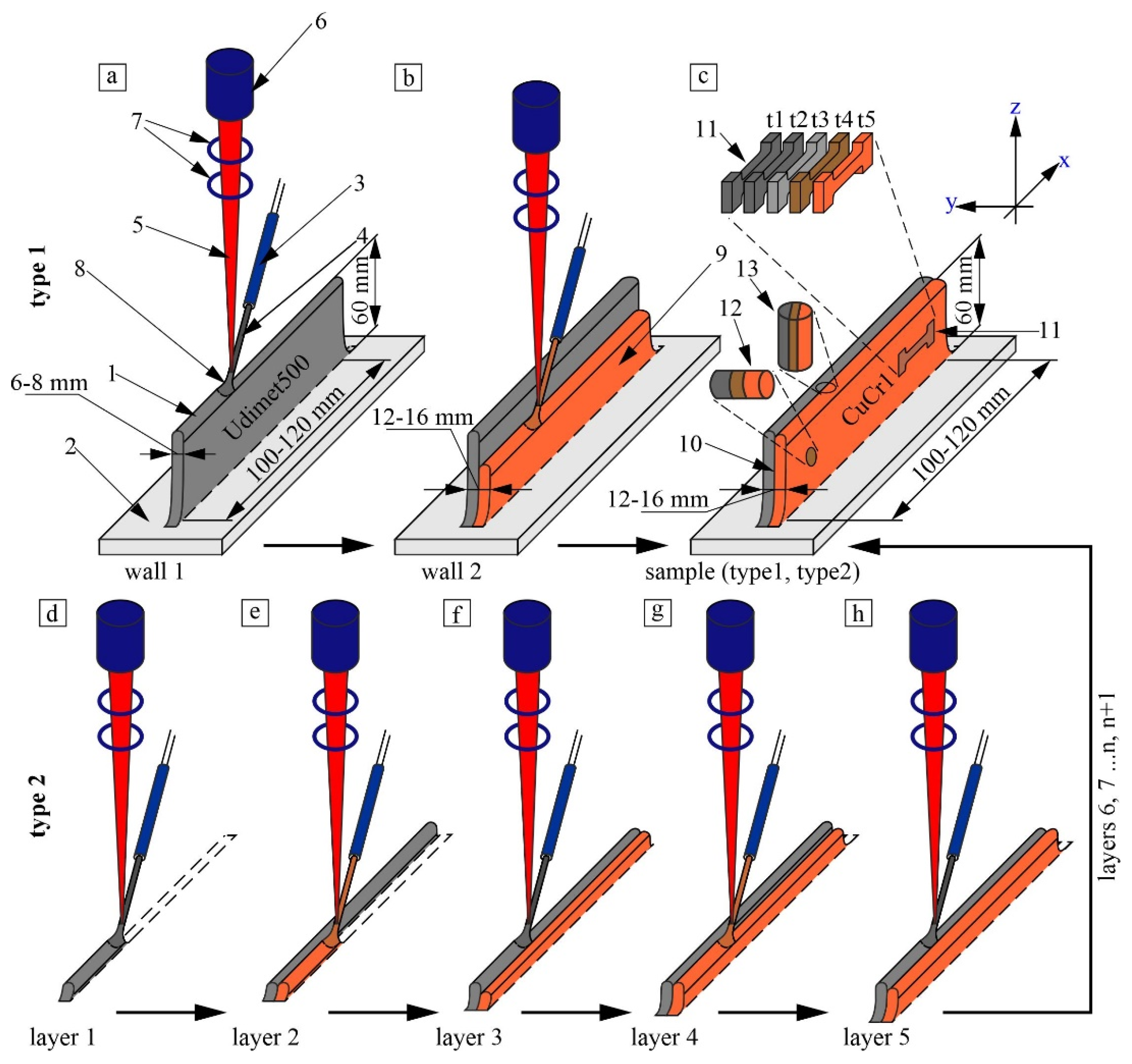
The printing strategies of bimetallic composite samples are schematically represented in
Figure 2. Sample 1 was grown on the surface of steel substrate 2 using wire 4 fed through nozzle 3 and melted by electron beam 5. The beam was emitted from source 6 and focused in the printing area by magnetic focusing system 7 to form melt pool 8. Two parts 1 and 9 formed bimetallic wall 10. Various specimens were cut from the wall for metallographic studies and for determining the mechanical properties in tensile tests 11 and compression tests 12, 13.
Type I samples were obtained by sequential formation of two parts of nickel alloy (
Figure 2a) and copper alloy (
Figure 2b) with an interface between them (
Figure 2c). Type II samples were formed on the steel substrate by alternately deposited nickel and copper alloy layers (
Figure 2d–h): the first nickel layer (
Figure 2d) and copper layer (
Figure 2e), the second nickel layer (
Figure 2f) and copper layer (
Figure 2h), and so on. The cycle was repeated (
Figure 2h) until the required height of the bimetallic wall was reached (
Figure 2c). Type II sample also consisted of two separate parts of nickel and copper alloys, but with a wider interfacial transition zone between them.
Test specimens for macro- and microstructural studies were cut from the grown vertical walls using a DK7750 electrical discharge machine. Specimens for macrostructural studies were cut from the bimetal cross section. They were ground and polished by a standard method and then surface etched in a solution of 8 gr CuSO4 + 40 mL C2H5OH + 40 mL HCl. Macroscopic images of the specimens were taken with a Pentax K-3 camera with a lens focal length of 100 mm. Optical studies were carried out on an Altami MET-1C metallographic microscope (Altami, St. Petersburg, Russia) and an OLYMPUS LEXT confocal microscope (Olympus NDT, Inc., Waltham, MA, USA). The elemental composition of the specimens was determined using a LEO EVO 50 scanning electron microscope (Zeiss, Germany) and a Thermo Fisher Scientific Apreo S LoVac scanning electron microscope with an analytical EDS system (Thermo Fisher Scientific, Waltham, MA, USA). X-ray structural analysis was performed on an X-ray diffractometer (DRON-7) using CoKα radiation at 0.05° increments and an exposure time of 10 s per step. Microhardness measurements were carried out by the Vickers method on an Affri DM8 microhardness tester (Affri, Italy). Tensile specimens with the gauge dimensions 12 × 1.5 × 2.7 mm3 and compression specimens in the form of cylinders 5 mm in diameter and 10 mm in length were used to investigate mechanical characteristics. Tests were performed on a UTS 110M universal testing machine. The strain rate was 1.4 × 10⁻³ s−1. The mechanical properties were investigated along and across the bimetallic interface.
3. Results
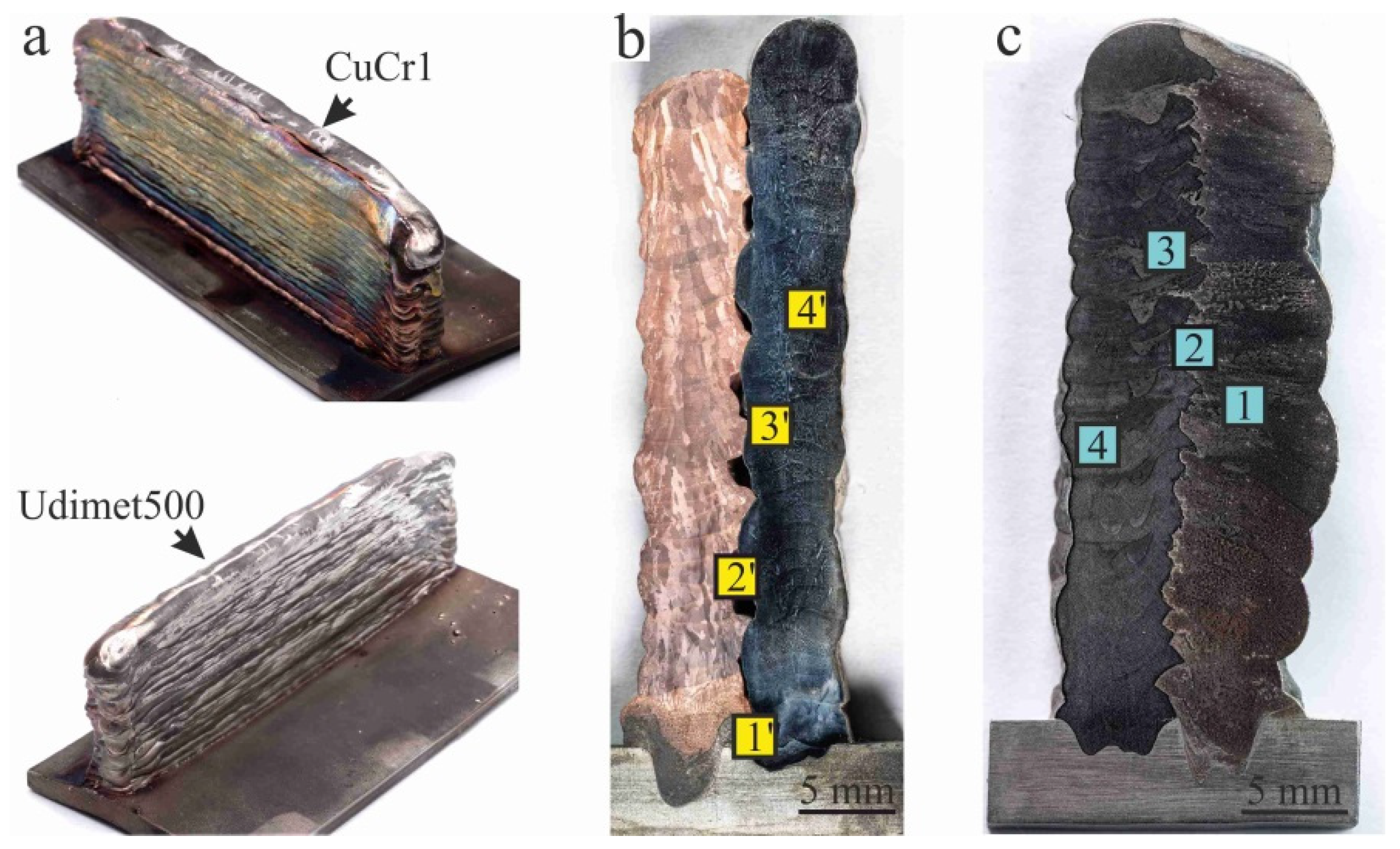
The general view of the vertical walls produced by electron beam additive manufacturing using wires of heterogeneous heat-resistant nickel-based superalloy Udimet 500 and copper alloy CuCr1, is shown in
Figure 3a. A visually observed characteristic of this manufacturing technology is the interlayer boundaries in the samples [
37]. Printing the vertical wall by strategy I leads to the formation of macrodefects (
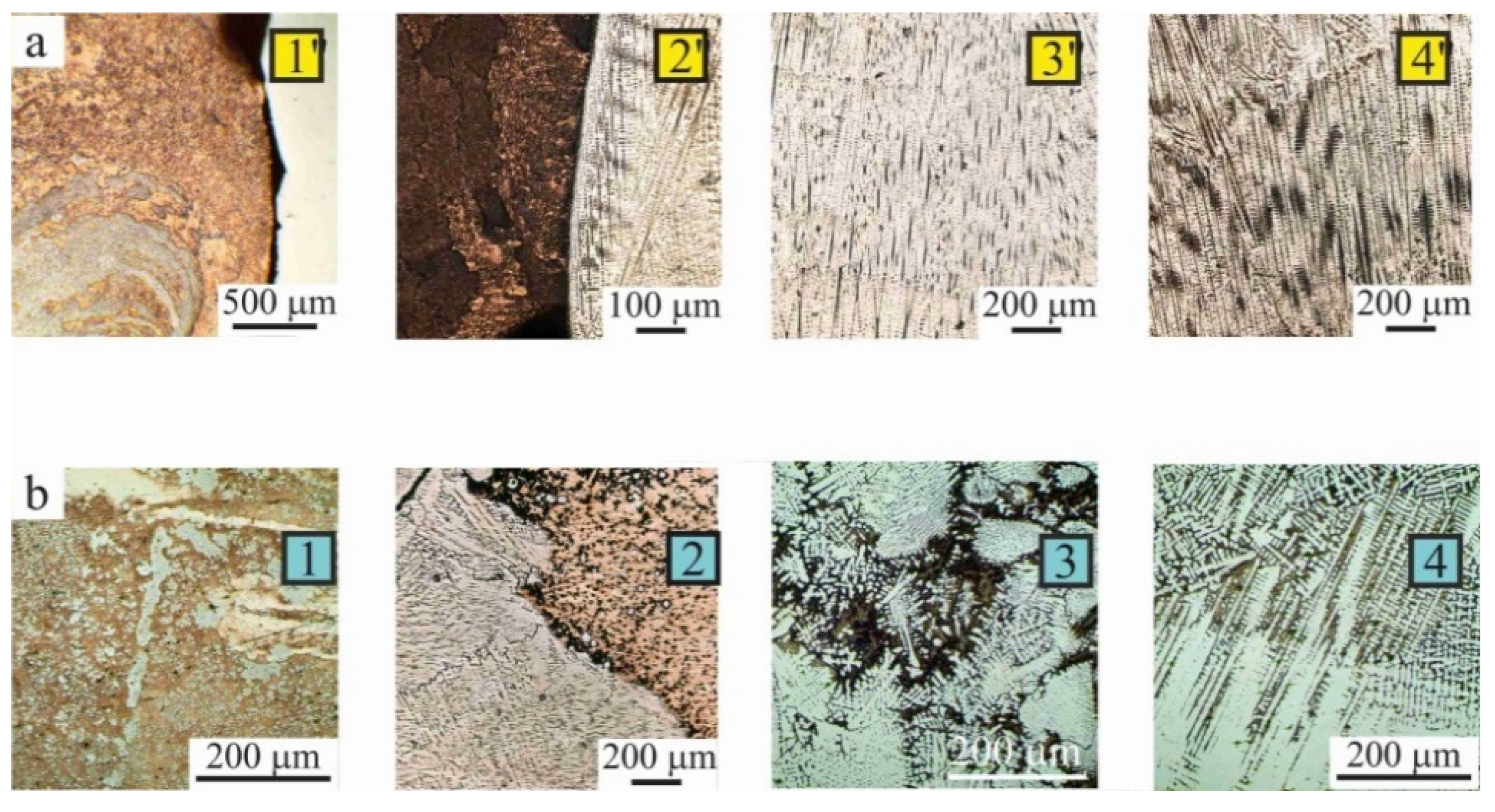
Figure 3b). This is due to insufficient heating of the solidified nickel wall during copper wire deposition; copper alloy flows away from the nickel wall, which causes a difference in the height of the copper wall. This is affected by a 1.5-fold difference in the melting temperature and a 17-fold difference in the thermal conductivity of the materials used. Therefore, the temperature is not sufficient to melt the deposited Udimet 500 layers. In addition, printing imposes high heat transfer conditions during the deposition of CuCr1 layers; the nickel alloy layers do not have time to melt under such thermal conditions. This leads to the formation of voids up to 1.5 mm in width and up to 3 mm in length at the Udimet 500/CuCr1 interface (
Figure 3b and
Figure 4a, region 1′). Despite the presence of voids, there are junction zones between the dissimilar materials with a sharp interface (
Figure 4a, region 2′). As the electron beam current increases, allowing Udimet 500 to melt and spreading of copper. This leads to uneven layers, distortion of sample geometry, and formation of internal void-like defects. In the initial stages of copper alloy deposition, the copper alloy mixes with the substrate material, and equiaxed grains of size 50 μm are formed. As the vertical wall grows, the grains are slightly elongated to an average length of 200 μm and width of 80 μm. Nickel alloy shows the morphology of a grain-dendritic structure. This morphology includes both equiaxed (
Figure 4, region 3′) and columnar grains (
Figure 4, region 4′). According to Hunt’s theory of crystallization [
37], a dendritic structure is formed during the deposition of Udimet 500 layers.
The vertical wall printed by strategy II has a defect-free interface (
Figure 3c). This is due to the fact that near to the already solidified copper alloy the layers from the nickel alloy Udimet 500 (the melting temperature of which is higher) were deposited.
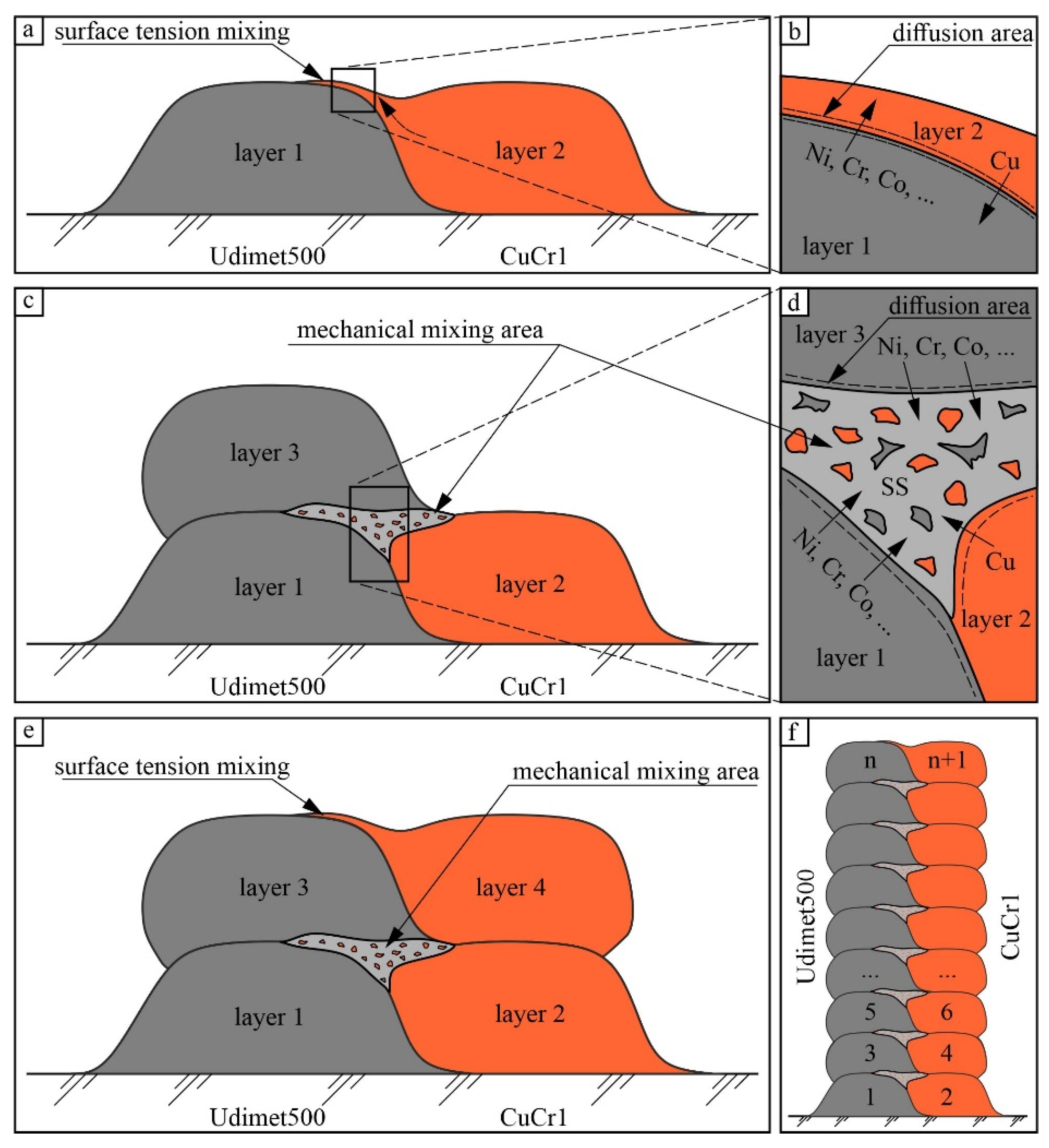
Strategy II results in nonuniform mixing of nickel and copper alloys due to differences in the material densities and Marangoni convection (
Figure 3b). Copper regions exhibit randomly shaped inclusions of heat-resistant nickel alloy (
Figure 4b, region 1). One can see interfacial interaction between the copper and nickel parts (
Figure 4b, region 2). The mixing of nickel and copper alloys is observed when considering copper inclusions in the nickel matrix (
Figure 4b, region 3). A mesh structure with uniform copper distribution is formed in the nickel alloy area. The interphase boundaries of inclusions are sharp, without transition regions. The number of nickel alloy dendrites increases away from the transition zone and, as a consequence, the concentration of copper decreases (
Figure 4b, region 4). During filament printing, copper inclusions are distributed along the boundaries of the grain structure. As the operating temperature increases, copper alloy melts, while the nickel matrix remains a solid solution. At the same time, there is stirring in the liquid state. The structure develops based on primary crystallization of austenite dendrites, followed by solidification of copper between the dendrites. Copper conglomerates are observed in the interdendritic area near the nickel matrix interface. These accumulations increase the effective heat dissipation from the crystallizing nickel matrix, thereby increasing the temperature gradient, which in turn can suppress the growth of secondary dendrite arms, or prevent the formation of dendritic morphology at all (
Figure 4b).
Two types of interfaces can be detected on the cross-section surface of the samples: a sharp interface extending up to 2.5 mm (
Figure 3b), and a smooth interface extending to 10 mm (
Figure 3c). This is a specific feature of bimetal formation in the present work.
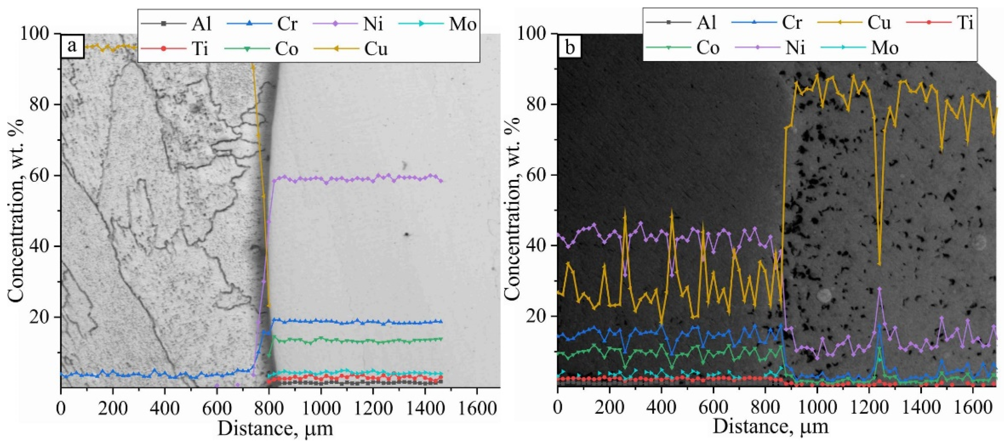
Figure 3c shows that the interface is distinct, with no defects such as cracking or delamination, confirming a strong adhesion between the materials. Nickel-based superalloy exhibits a narrow layer of thin dendritic structure near the interface. The sharp interface is characterized by a low degree of mutual dissolution of the components (
Figure 5a). Away from the interface, the nickel matrix shows a concentration of elements comparable to the raw material composition (
Figure 5a). This structure of the transition zone is optimal in terms of preserving the high strength of nickel alloy and the thermal conductivity of copper alloy.
The mutual dissolution of nickel and copper alloys was most intense in type II samples due to the chosen printing strategy II (
Figure 5b). The components diffused more readily during deposition of copper layer next to nickel layer at a sufficiently high temperature of the latter. The subsequent nickel layer partially melted the underlying nickel layer and a small part of its interface with the copper layer, leading to mechanical mixing of the components. This led to a 25% decrease of Cu content in the nickel region and a 20% decrease of Ni content in the copper region. As a result, an extended interface zone was formed, as shown in
Figure 5b.
X-ray diffraction analysis was performed in areas at different distances from the Udimet 500/CuCr1 interfaces (
Figure 6a).
Figure 6a shows three characteristic X-ray diffraction patterns used to determine the qualitative phase composition. XRD patterns of Ni matrix, Cu matrix, and interface were taken in the areas of nickel alloy, copper alloy, and Udimet 500/CuCr1 interface, respectively. It was found that the bimetallic sample consists of nickel matrix, copper matrix, and their combination at the Udimet 500/CuCr1 interface, i.e., crystallization occurs without the formation of additional phases. However, the corresponding angular positions of the Ni and Cu reflections differ depending on the distance of the analyzed region. It is known [
38] that the dissolution of alloying elements in the matrix induces a change in its lattice parameter. In our case, the matrix materials are nickel and copper, and the alloying elements mostly affecting the matrix lattice parameter are Cr and Mo. The dissolution of alloying elements in the zone bordering the Udimet 500/CuCr1 interface can be traced by plotting the dependence of the matrix lattice parameter (Ni and Cu) on the distance from the interface (
Figure 6b). To do this, five samples were taken: two samples cut from the nickel alloy area, two samples cut from the copper alloy area, and one sample cut from the Udimet 500/CuCr1 interface. The lattice parameter (a, Å) was estimated by an X-ray extrapolation method. It was found that the nickel lattice parameter in the nickel alloy region was 3.5844 ± 0.0019 Å, and the copper lattice parameter in the copper alloy region was 3.6059 ± 0.0011 Å. In the Udimet 500/CuCr1 interfacial region, the lattice parameter of the copper matrix increased and the lattice parameter of the nickel matrix decreased, as shown in
Figure 6b.
Figure 6b also shows an XRD quantification of the elemental composition in the nickel and copper phases of each sample. By correlating the lattice parameter and elemental composition plots, we can see that Cr and Mo atoms are present in the copper component of the interface. In this case, the Cr and Mo atoms have a larger atomic radius than the Cu atom, which in turn increases the lattice parameter of the copper component [
38]. On the other hand, Cr and Mo atoms diffusing from nickel alloy induce a decrease in the lattice parameter of the nickel component, which can be observed in
Figure 6b. As a result, at the interface we have a homogeneous content of alloying elements in the copper and nickel matrices, but a greater mismatch of their crystal lattices. This can cause stress fields at the phase boundaries or, vice versa, create incoherent boundaries between the copper and nickel phases. This plays a key role in the design of parts for cyclic thermal operating conditions.
Microhardness and compression measurements were performed and the results obtained were compared with the structural data.
Figure 7a shows the results of microhardness measurements performed on the sample cross sections from
Figure 3b,c.
As can be seen from
Figure 7a, there is a difference between the samples obtained by printing strategies I and II. Type I sample showed no mutual penetration of alloying components. The red curve in
Figure 7a displays the microhardness values of copper and nickel alloys without mutual penetration. The situation is different for type II sample. As shown above, the chemical elements of nickel and copper alloys in type II sample penetrated the interface. As follows from the microhardness distribution curve (
Figure 7a), the presence of copper in the nickel alloy area decreases its microhardness, and the presence of nickel alloy chemical elements in the copper region increases the copper alloy hardness. An analysis of micromechanical properties revealed jumps in microhardness above the average values for the copper and nickel regions. This is confirmed by the change in the size of the indentations made by a diamond pyramid indenter (
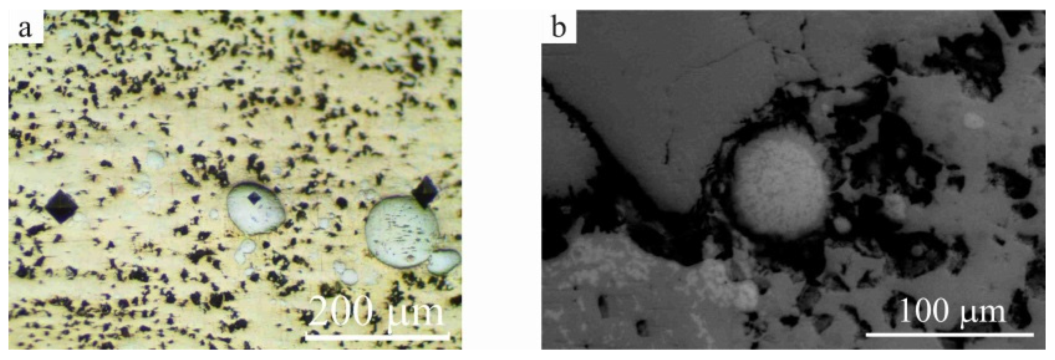
Figure 8a). The copper alloy region exhibits inclusions with an average size of 50 μm formed on the basis of alloying elements of heat-resistant nickel alloy 29.5Mo + 27.8Cr + 18.8Ni + 16.3Co + 6.3Cu + 1.3Ti. The interphase boundaries of the inclusions are sharp, without transition regions (
Figure 8b). These particles have an increased microhardness value of 790 HV (
Figure 8).
Compression tests were conducted only on type II samples. This decision was motivated by the presence of numerous defects in type I samples, which caused sample failure.
Figure 7b shows the compression test results for type II samples loaded in mutually perpendicular directions. Only two loading curves corresponding to the highest and lowest stresses are shown. As can be seen from the curves, sample deformation occurs at much lower stresses under a load applied normally to the interface as compared to loading parallel to the interface.
Despite the heterogeneous structure of type II samples, their strength properties are sufficiently high (
Figure 7c). The strength in the nickel alloy region is up to 1073 MPa and that in the copper alloy region is up to 279 MPa. The average ultimate strength in the transition zone is up to 754 MPa, but the relative elongation to failure in this zone is the lowest.

