Article

Effects of Bismuth on the Microstructure, Properties, and Interfacial Reaction Layers of Sn-9Zn-xBi Solders

1
Faculty of Materials Science and Engineering, Kunming University of Science and Technology, Kunming 650093, China
2
Research and Development Center, Yunnan Tin Group (Holding) Company Limited, Kunming 650106, China
*
Authors to whom correspondence should be addressed.
Metals 2021, 11(4), 538; https://doi.org/10.3390/met11040538
Submission received: 8 March 2021 / Revised: 22 March 2021 / Accepted: 24 March 2021 / Published: 26 March 2021

Abstract

:
In electronic packaging, Sn-Zn lead-free solder has great application prospects. Sn-9Zn-xBi alloys were obtained by smelting. This paper details a systematic study of the effect of Bi on the microstructure, melting behavior, wettability, mechanical behavior, antioxidant properties, and electrical conductivity of Sn-9Zn-xBi alloy, as well as the interfacial reaction in Sn-9Zn-xBi/Cu joints. The coarse Zn-rich phase became larger with an increase in the addition of Bi, which is harmful to the oxidation resistance of the solders. The melting temperature, solidus temperature, and liquidus temperature decreased with the increase in the addition of Bi, but the melting range increased. Adding a proper amount of Bi could substantially improve the spreading rate of Sn-9Zn, but reduce its oxidation resistance. Because of the solid solution effect of Bi element, the tensile strength of the Sn-9Zn solders could be enhanced, but the plastic and electrical conductivity was decreased. The IMC layer of the Sn-9Zn and Cu joints consisted of the ε-CuZn5 phase and the γ-Cu5Zn8 phase. With an increase in the Bi element, the thickness of the interfacial reaction layer was firstly increased. When the Bi element content exceeded 3 wt.%, the inhibitory effect of the aggregated Bi elements on the formation of IMC was greater than the positive effect of the longer reaction time, and the thickness of the IMC decreased.

Graphical Abstract

1. Introduction

Solder plays a various crucial roles in electronic packaging, such as in electrical connections and mechanical connections. Because of its advantages of low melting point, excellent wettability, good weldability, and low price, Sn-Pb alloy become the most popular solder in electronic packaging industries [1]. However, because Pb and its compounds are toxic, it would cause adverse effects on the natural environment and human body, thus the use of Pb and Pb-containing products are banned in most countries [2]. Currently, the lead-free solders that are studied mainly include Sn-Ag-Cu (SAC), Sn-Zn, and Sn-Cu alloys [3,4]. Sn-Ag-Cu alloy shows a good performance, which has made it a mainstream lead-free solder [5,6]. However, the melting point of SAC alloy is high due to the addition of Cu and Ag, and electronic components are sensitive to high temperatures, which limits the broad application of these solders. In addition, with the development of the electronics industry, such as mobile phones and other handheld devices, the problems of the high cost and poor anti-drop properties of SAC solder are prominent.
Sn-Zn solder has great application prospects due to its advantages, such as the low cost of raw materials and low melting point. The melting point of Sn-9Zn solder is only 198 °C, close to that of the Sn-Pb alloy [7]. However, Zn is a more active, liquid Sn-Zn alloy that has a high surface tension, and zinc oxide is inclined to agglomerate on the liquid surface; this is the reason for the poor oxidation resistance and wettability of the Sn-Zn alloy [8]. Studies have shown that adding Bi, Nd, Ag, and Ga can improve the wettability and tensile strength of Sn-Zn solder [9,10,11,12]. Mahdavifard et al. [13] investigated the effect of adding Bi on the properties of Sn-1.0Ag-0.5Cu-Fe solder; the results showed that Bi will increase the strength of the solder and reduce the total elongation by reducing the Cu6Sn5 phase. Meanwhile, Eid et al. [14] reported that adding Sb to Sn-6.5Zn-0.3Cu alloy will enhance the tensile properties as a result of the solid solution and Sb2ZnSn IMC formation. As reported by Hu et al. [15], Bi element can lower the melting point and improve the mechanical properties and welding performance of the Sn-0.7Cu alloy. El-Daly et al. [16] reported that the 1.0 wt.% Bi element addition in the Sn-6.5Zn alloy can decrease the size of the α-Zn and refine and modify its microstructure. Zhao et al. [17] reported that during the high-temperature aging process, the rapid solidification process significantly inhibited the growth of the interface intermetallic compound layer of the Sn-8Zn-3Bi/Cu joint and improved the high-temperature stability. However, excessive Bi element is prone to segregation at the junction of solder and Cu, resulting in a sharp drop in the creep strength and shear strength of the solder joint [9]. There have been many studies on the effect of the addition of Bi element on solder alloys, but they mainly focus on the melting characteristics, wettability, and mechanical strength of the alloy. However, there are few studies on the oxidation resistance and electrical conductivity of solder with Bi element.
Based on the above research results, Bi as a potential alloying element was chosen to promote the comprehensive properties of Sn-9Zn alloy in this paper. Various properties of Sn-9Zn-xBi solder were tested, such as its mechanical properties, thermal properties, oxidation resistance, wetting properties, and electrical conductivity, which were investigated systematically. In the context of the interfacial reliability of solder joints, the interfacial IMC thickness is expected to influence the joints’ strength and subsequent mechanical properties. The interfacial reaction in the Sn-9Zn-xBi/Cu joints has been studied.

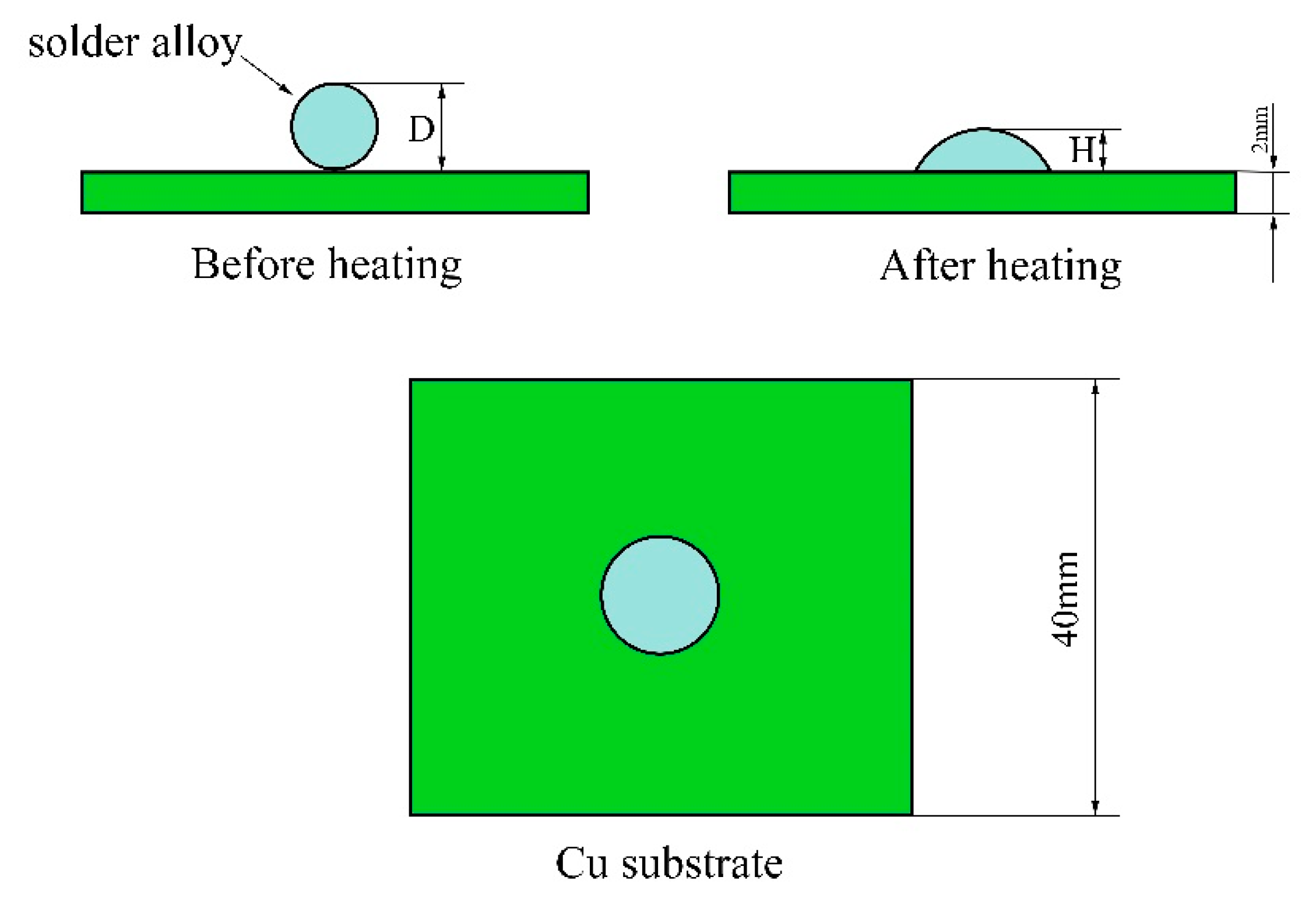
2. Materials and Methods

The Sn-9Zn-xBi alloys were obtained by smelting. First of all, we put KCl/LiCl salt in the corundum crucible and heated the KCl/LiCl salt to 500 °C in a muffle furnace to obtain melting salt. Secondly, pure Sn, Zn, and Bi were placed into a corundum crucible. The alloys were heated at 500 °C for 1 h to promote melting. The alloys were stirred 1 min every 10 min during the heating process. The actual chemical composition of the Sn-Zn-xBi alloys was measured by inductively coupled plasma (ICP) analysis. The results are shown in Table 1.
To observe the microstructure of the solder alloys, samples with a size of 10 mm × 5 mm × 5 mm were cut from the solder ingots. After grinding and polishing, the samples were corroded with 5% HCl and 95% (vol.%) C2H5OH solution for 5–10 s. The microstructure was observed using scanning electron microscopy (SEM, Tescan-vega3, TESCAN, Brno, Czech Republic). The melting characteristics of the Sn-9Zn-xBi solder alloys were analyzed using a differential scanning calorimeter (DSC, TA 25, TA, New Castle, DE, USA). The weight of the solder specimen used in the test was 5 mg, and the experiment was performed under a high-purity nitrogen atmosphere. The spreading rate was used to characterize the wettability of the solders. The spreading experiment was carried out according to the China National Standard GB11364-2008. Copper substrates (40 mm × 40 mm × 2 mm) were ground with sandpaper and polished to achieve a relatively smooth surface. The solder spheres (0.3 g) were placed on Cu substrates with SP-05 active flux, and they were heated to 250 °C and kept for 90 s in an air atmosphere. The schematic diagram of the wetting test process is shown in Figure 1. The spreading rate can be calculated by the following formula:
K = (D-H)/D × 100%,
where K is the spread rate; H is the height of the solder spread on the Cu substrate surface, in millimeters (mm); D is the diameter of the solder sphere, in millimeters (mm). The wetting angle of the Sn-9Zn-xBi solder alloy was observed by SEM and the wetting angle was measured. The microstructure and chemical composition of the interface of Sn-9Zn-xBi/Cu joints was determined by electron probe microprobe analysis (EPMA). Thermal gravimetric analysis was used to characterize the oxidation resistance of the solders. The sample was heated to 240 °C at the rate of 10 °C/min and kept there for 120 min. The mechanical behavior of the solder was evaluated by a tensile test, which were performed at an ambient temperature on a universal testing machine (Autograph AG-X, Shimadzu, Kyoto, Japan); the stretching rate was 1 mm/min. The tensile test was carried out according to the China National Standard GB6397-88. The electrical resistivity of the Sn-9Zn-xBi solder alloy was measured by a four-point prober. The dimension of the specimen was 0.08 mm high, 1 cm wide, and 2 cm long, with a probe spacing of 1 mm, while the corresponding voltage that had dropped across the solder alloy was measured with a 2A current. The sample’s electrical resistivity can be calculated by the following formula:
ρ = CV/I,
where ρ is electrical resistivity; C is the probe correction factor, determined by the probe spacing and specimen size; V is voltage; and I is current. For the above properties of the solders, at least three specimens were tested for each alloy and the average values are reported.

3. Results and Discussion
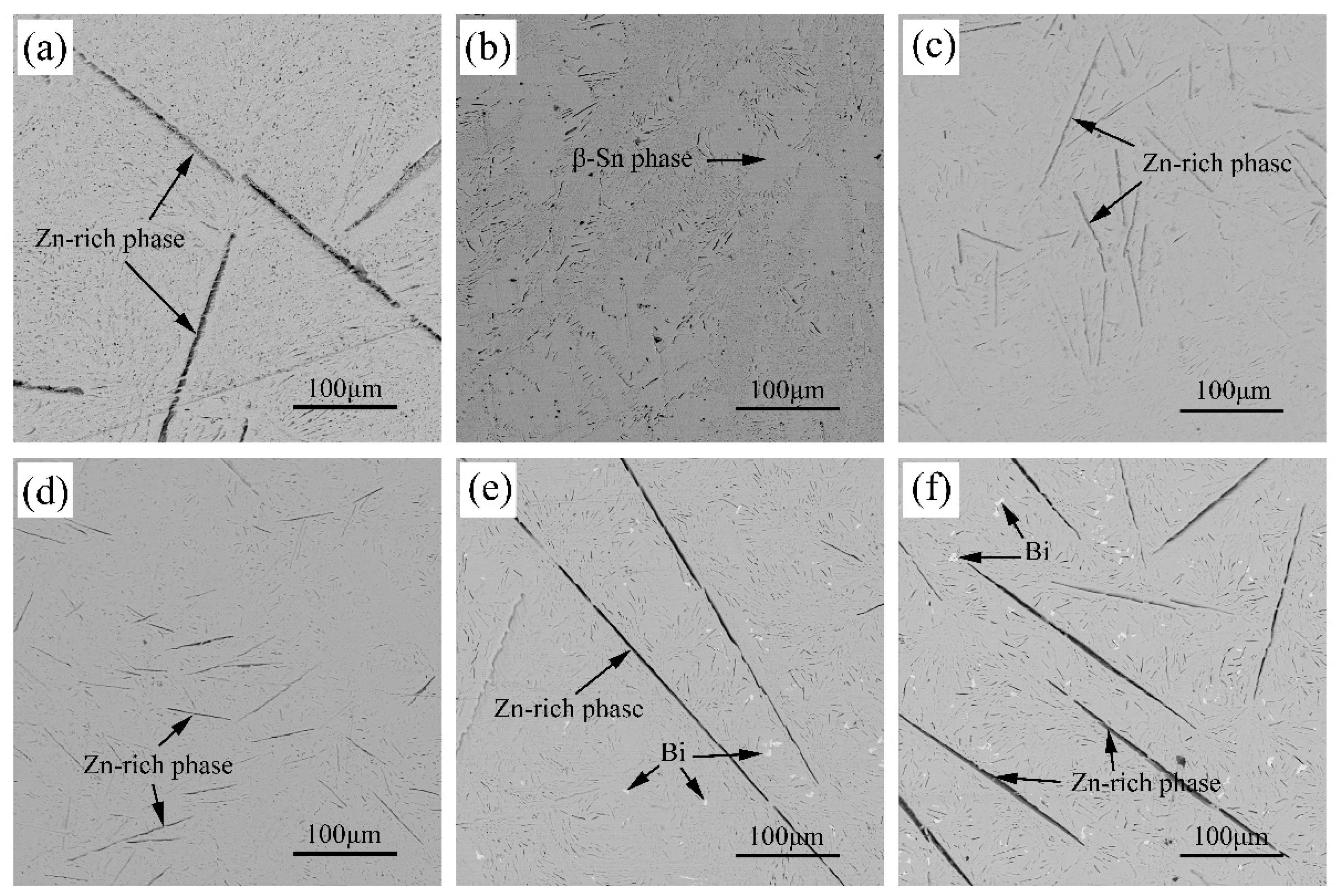
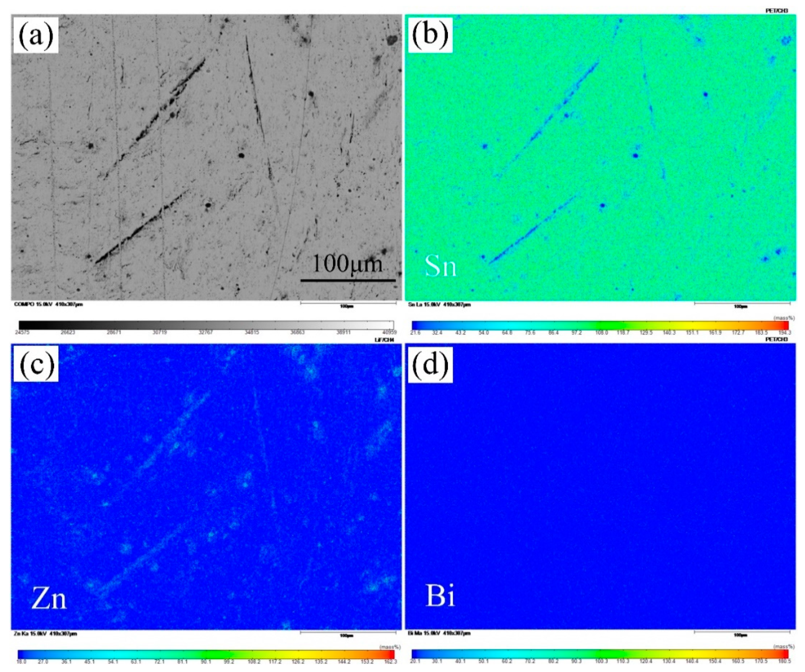
3.1. Microstructure

Figure 2 shows back-scattered electron (BSE) images of the Sn-9Zn-xBi (x = 0, 1, 2, 3, 4 and 5) alloys. EPMA element mapping analysis was carried out for the Sn-9Zn-3Bi and Sn-9Zn-5Bi alloys to clarify the composition of the matrix phase, white phase, and black phase. Sn-9Zn-3Bi and Sn-9Zn-5Bi alloys map analyses are shown in Figure 3 and Figure 4. The microstructure of Sn-9Zn solder is mainly composed of a light gray β-Sn phase, Sn-Zn eutectic mixture, and coarse black acicular Zn-rich phase. The Sn-Zn eutectic mixture is in the form of an alternate distribution of the Sn phase and the fine acicular Zn-rich phase. When Bi was added, compared to the microstructure of the Sn-9Zn alloy, the microstructure was greatly changed in terms of the size, morphology, and distribution of the β-Sn phase, Zn-rich phase, and Sn-Zn eutectic. When the amount of Bi element was less than 3 wt.%, Bi particles could not be observed in the structure, and Bi was uniformly distributed in the Sn base. Bi atoms could endorse the solidification process of the solder promptly through the heterogeneous nucleation at Bi particles, which results in the fine microstructure and random distribution of eutectic colonies. After adding 1 wt.% of Bi element, the coarse acicular Zn phase in the matrix disappeared and transformed into a finer acicular precipitated phase distributed on the β-Sn matrix. After adding 2 wt.% of Bi element, it was found that part of the Zn had a tendency to transform into a coarse Zn-rich phase. Adding 4 wt.% of Bi, the coarse Zn-rich phase appeared and white granular Bi precipitated from the Sn matrix, which suggested that the solubility limit of Bi element in the Sn matrix is more than 3 wt.%. Adding 5 wt.% of Bi, the number of coarse Zn-rich phases and white Bi particles increased.

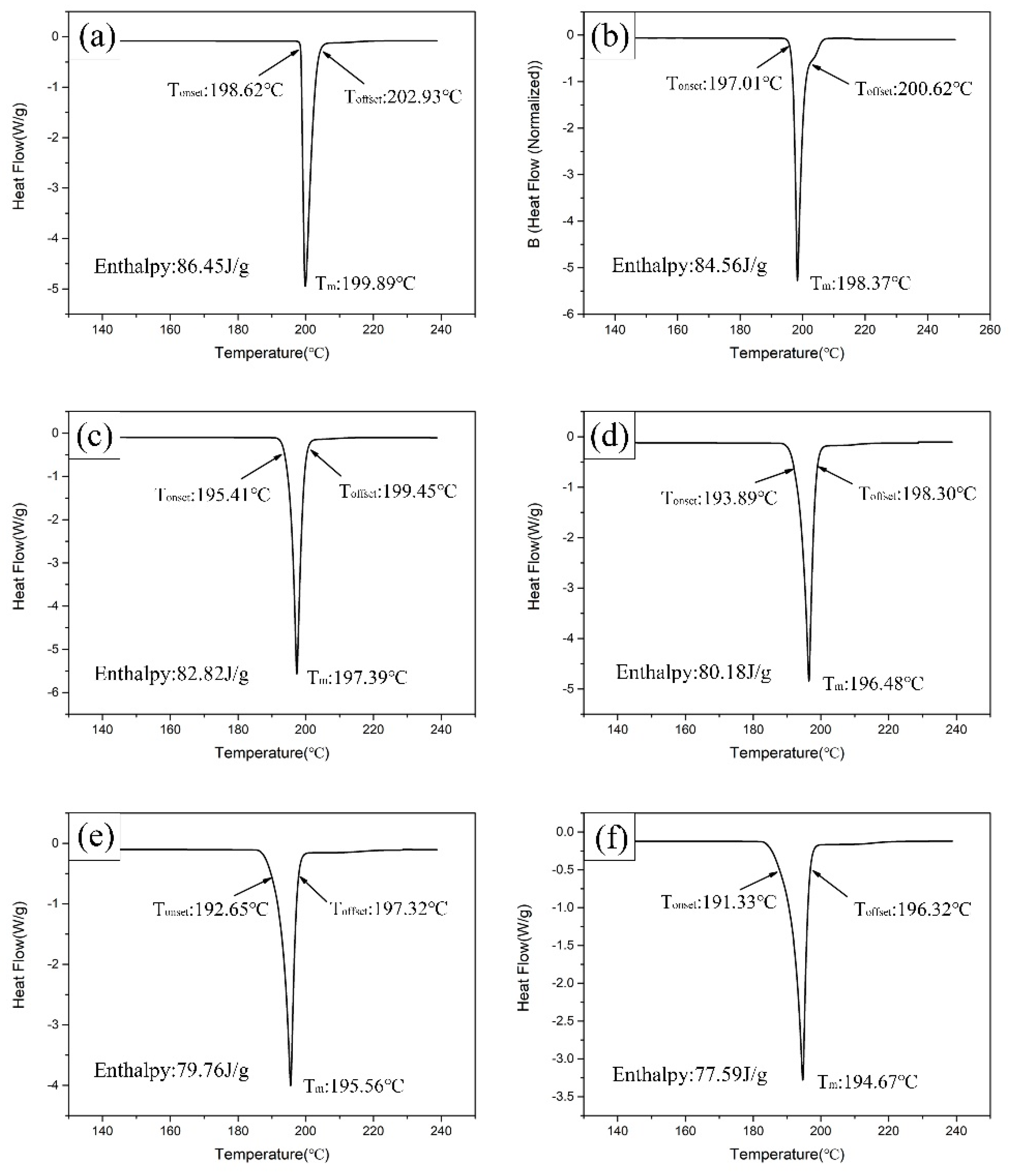
3.2. Melting Properties
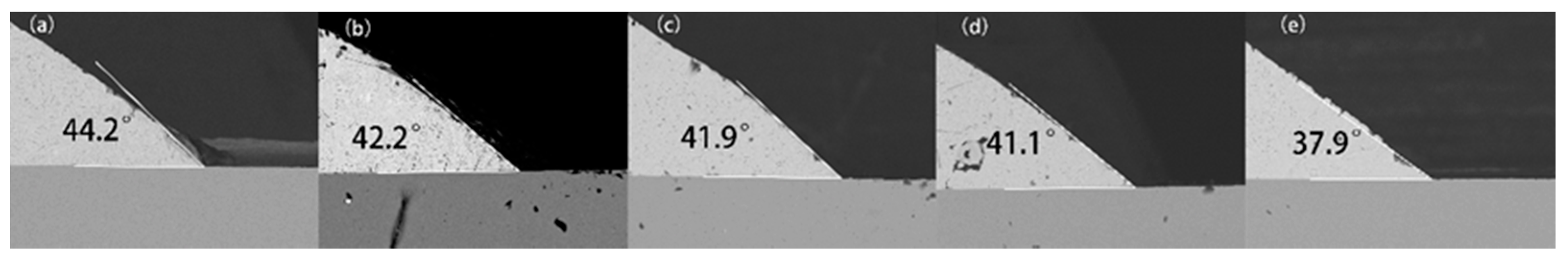
For electronic packaging solder, the melting point and pasty range are important technical indicators to measure the soldering performance of solder. The solder with a high melting temperature requires a high soldering temperature, may cause failure of electronic components. Figure 5 shows the results of the DSC analysis. The DSC results are noted and compared in Table 2. Only one endothermic peak in each DSC curve was observed (i.e., the chemical compositions of the investigated solder alloys are near eutectic). Addition of Bi would dropping the melting point, solidus temperature, liquidus temperature. The melting temperature of Sn-9Zn is 199.89 °C. As Bi content increased to 5 wt.%, the melting temperature of alloy dropped to 194.67 °C. Tm is the melting point. Tonset is the solidus temperature, Toffset is the liquidus temperature. The temperature range of the pasty(Toffset-Tonset) slightly expands with the addition of Bi. In the nearly eutectic composition, the pasty range is small and a homogeneous phase is obtained through reflow process which inhibited an occurrence of segregation during solidification. The pasty range of Sn-9Zn-1Bi is 3.61 °C; whereas, the addition of 5 wt.% Bi increased the pasty range to 4.99 °C. A smaller melting range could reduce the porosity of the solder joints and improve the reliability of the solder joints. A large melting range increases the tendency towards porosity and hot tearing due to the effect of alloy shrinkage and differential thermal contraction during solidification. In practical applications, a larger pasty range would increase the susceptibility of the solder to vibration during welding process [18]. Bi addition may form solid solution with Sn. Besides this, the eutectic temperature of Sn-Bi alloys is 139 °C, which could lower the melting point of the Sn-9Zn-xBi alloy.
The data as listed in Table 2. The decrease in enthalpy showed that Sn-Zn-xBi solder alloys (x = 0, 1, 2, 3, 4, and 5) can be melted with less energy.

3.3. Wettability

Good wettability is the key for the solder to complete welding. The solderability inspection of a solder mainly includes indexes such as spreading area, spreading rate, wetting angle, wetting time, and wetting power. In this study, the spreading rate was mainly used to investigate the wettability of each solder. The spreading rate is shown in Figure 6. The spreading rate of Sn-9Zn lead-free alloy is 58.76%. Adding Bi element, the spreading rate of solders gradually increases. When the addition of Bi was 5 wt.%, the spreading rate reached to 69.95%. It is indicated that the Bi element can improve the wettability of the Sn-9Zn solder.
The increase in the spreading rate can be attributed to the Bi element reduces the surface tension of the molten solder alloy. Erer et al. [19] also put forward similar conclusions. Their research shows that adding Bi to the SAC305 solder can improve the wettability of the solder.
The wetting angle of the solder alloy on the Cu substrate is shown in Figure 7. The contact angle of the Sn-9Zn-1Bi solder alloy is 44.2°. When the addition of Bi was 5 wt.%, the contact angle was reduced to 37.9°. It is indicated that the Bi element can improve the wetting performance of the Sn-9Zn alloy. The decrease in the contact angle can be attributed to the surface tension of the liquid solder alloy, where the spread of the liquid is influenced by the higher molecule force of attraction from a lower liquid surface tension. The Bi is a surface active element, which can significantly reduce the free energy of the molten Sn-9Zn alloy and the Cu substrate composition system, so that the activation energy of the wetting reaction is reduced. The decrease in activation energy allows the molten Sn-9Zn-xBi alloy to spread better on the Cu plate.

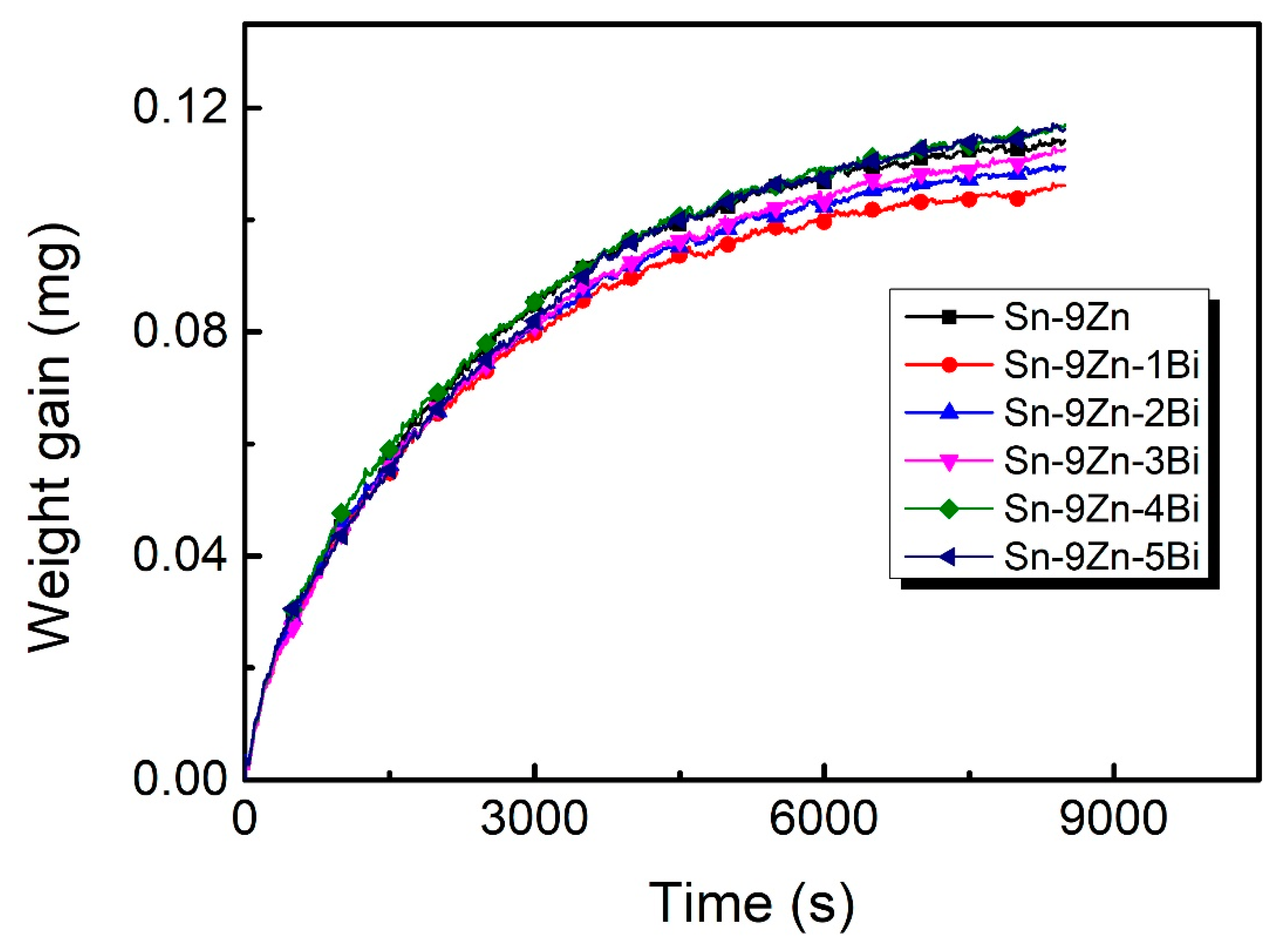
3.4. Oxidation Resistance

In order to test the antioxidant properties of Sn-9Zn-xBi alloy, thermal gravimetric analysis was used and the results are shown in Figure 8. We can find that the thermal gravimetric analysis curve of solder alloy rises faster in the early stage. With the extension of time, the curve tends to be flat, indicating that the weight gain of the alloy was faster in the early stage, and later the rate of the weight gain became slow. This is because Zn is easy to oxidize. When the solders are exposed to a high temperature environment, the zinc on the solders surface will quickly combine with oxygen and form zinc oxide. It is known that the phase transformation from Zn to ZnO is accompanied by a volume expansion. As the oxidation near the free surface progresses, the stress induced by the volume expansion of ZnO, which causes cracks to occur. The oxygen will enter the alloy along these cracks. Meanwhile, Zn will diffuse to the solder surface and continue to form zinc oxides [20]. As a result, the oxidation is exacerbated. In the later stages of the experiment, the oxidation of the alloy is mainly controlled by the diffusion reaction. Due to the increase in the thickness of Zn oxide film on the surface, the transfer of atoms is restricted, the oxidation rate of the Sn-9Zn-xBi alloy decreases. From the figure, it is also be found that the more Bi element is added, the thermal gravimetric analysis curve rises faster. It indicates that the Bi element content increases, the antioxidant performance of the solder become worse. When the content of Bi reaches 4 wt.%, the oxidation resistance is lower than that of the Sn-9Zn alloy. This is because after adding Bi, the alloy microstructure is apparently refined, and the Zn-rich phase is reduced. With the increase in Bi content, the coarse Zn-rich phase reappears, it will reduce the antioxidant performance of the solder. It is concluded that adding Bi can improve the antioxidant performance of the Sn-9Zn solder, but if the content of Bi is more than 3 wt.%, the antioxidant performance of the Sn-9Zn solder will decrease.

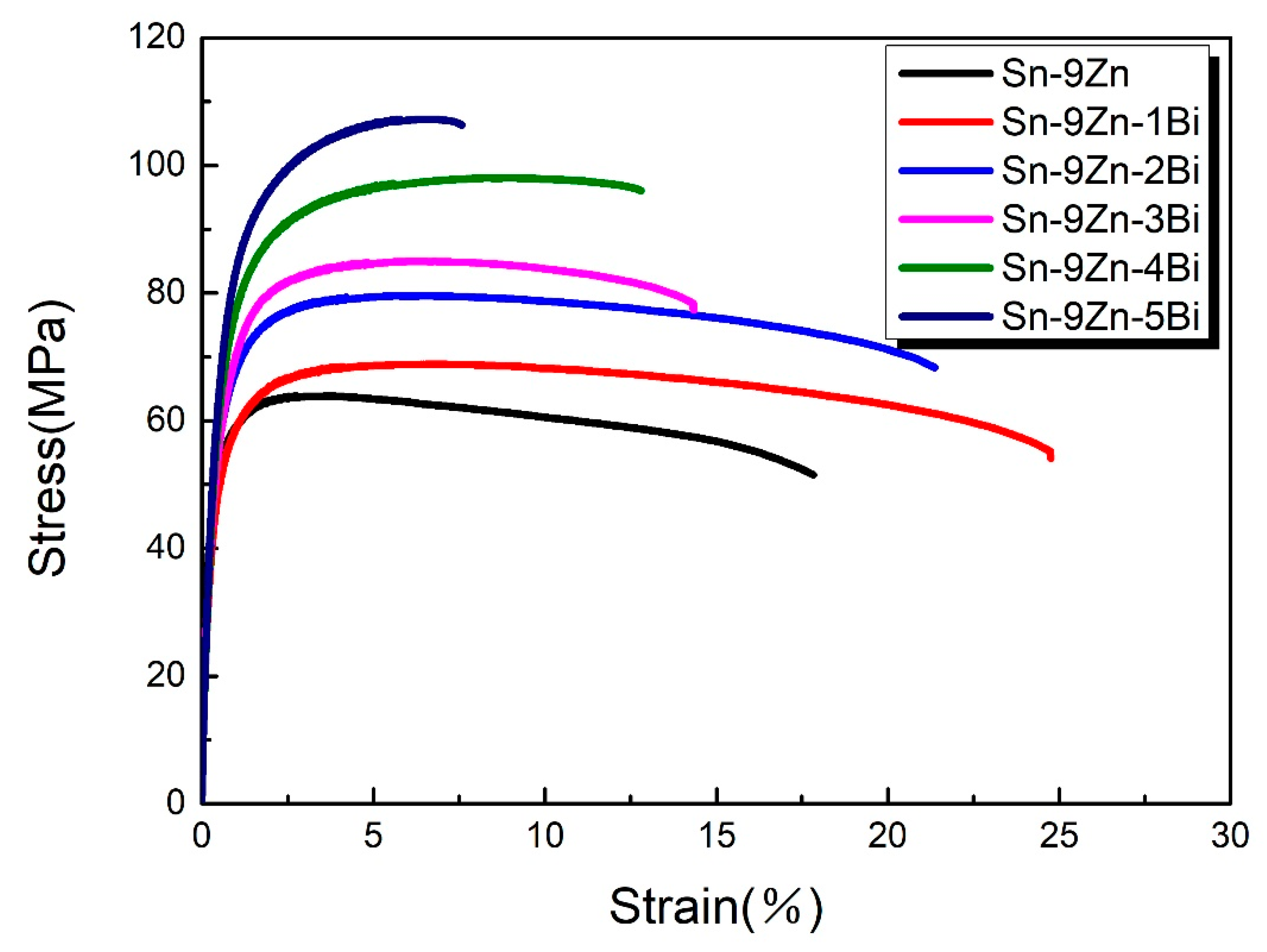
3.5. Mechanical Properties

Figure 9 shows the tensile curves of Sn-9Zn-xBi alloy. The relevant data are listed in Table 3. Bi element has great influence on the strength of Sn-9Zn-xBi alloys. Finding that the addition of Bi can significantly improve the tensile strength of the solder, the results indicate that the tensile strength of the alloys ranges from 61 to 107 MPa. With the addition of Bi, the tensile strength increased by about 43%. Bi element also has an obvious impact on the elongation of Sn-9Zn alloy. Adding Bi would increase the brittleness of the Sn-9Zn alloy. Sn-9Zn-1Bi solder’s elongation is the highest, reaching up to 25%. When the Bi content exceeds 3%, the plasticity of the alloy decreases significantly. Whereas Sn-9Zn-xBi (x = 1, 2 and 3) solders exhibit a higher elongation than the Sn-9Zn alloy, the strength is also increased. However, the alloying of Bi reported in many studies had a negative effect on the elongation of Sn-Zn-based alloys [16]. Referring to the microstructure analysis of Sn-9Zn-xBi alloys, the increase in tensile strength can be attributed to a solid solution hardening mechanism, and the refinement of Sn-9Zn-xBi (x = 1, 2 and 3) alloy microstructure also lead to the improvement of plasticity. Whereas, the increase in tensile strength of the Sn-9Zn-4Bi and Sn-9Zn-5Bi should be attributed to a precipitation hardening mechanism. With an increasing Bi content, Bi atoms would precipitate out from the matrix and produce a lot of brittle particles, which leads to a significant increase in strength and decrease in plasticity. Those massive precipitations in alloys, which are quite brittle, must be avoided because they will possible induce crack in the matrix under low stress or some cyclic stress under service conditions. Therefore, it can be concluded that both the solid solution hardening and precipitation of Bi are the main causes for the considerable change in the tensile strength and elongation of the Sn-Zn-Bi alloys.

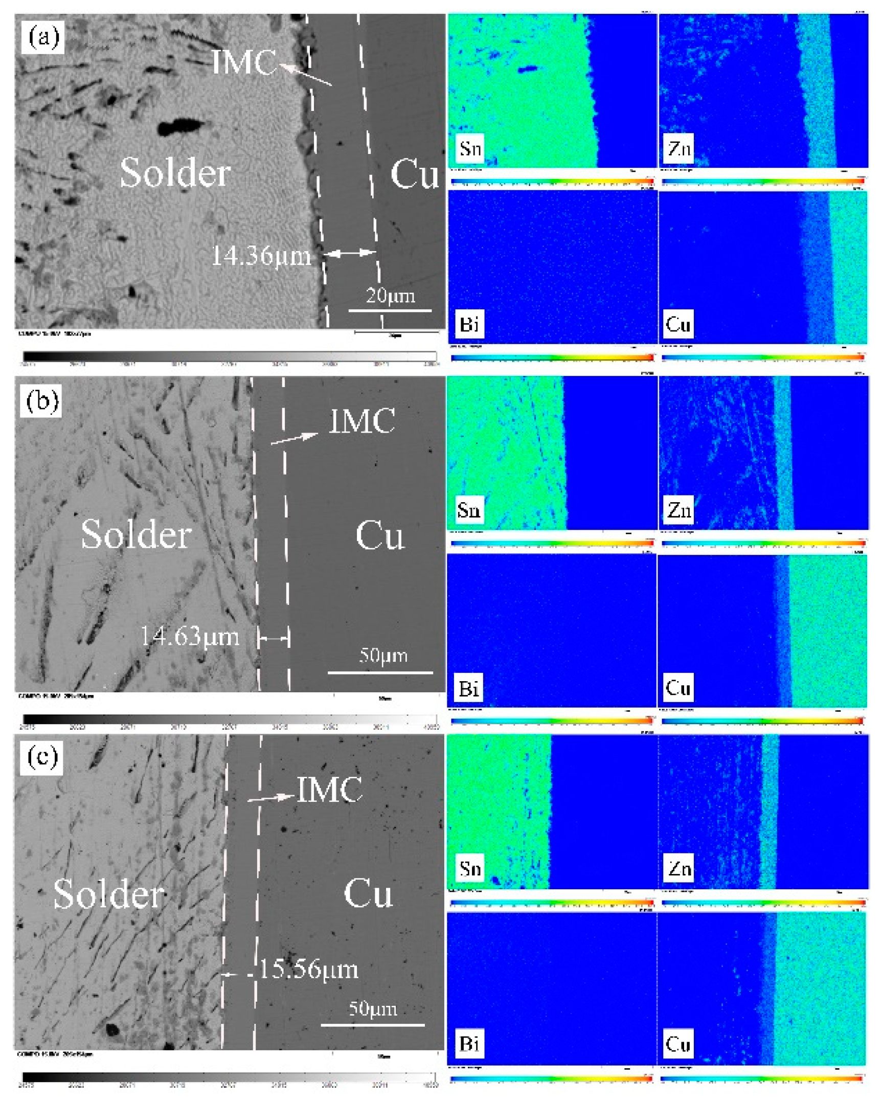
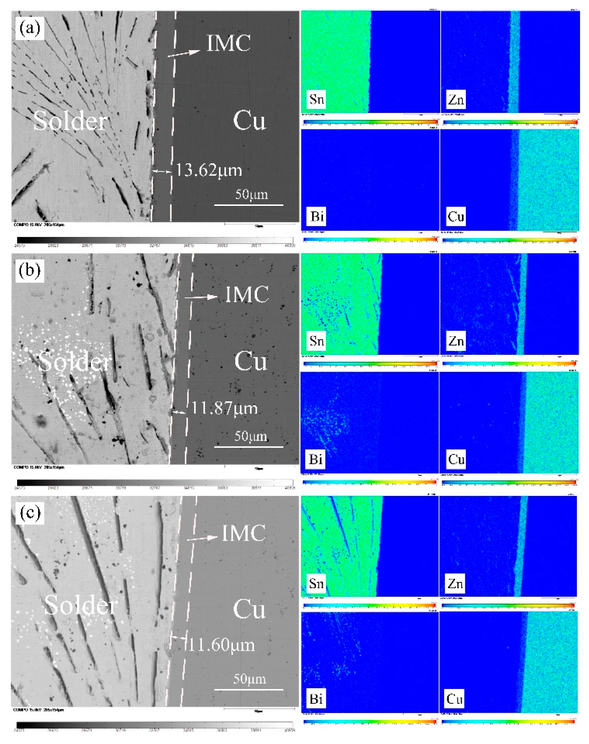
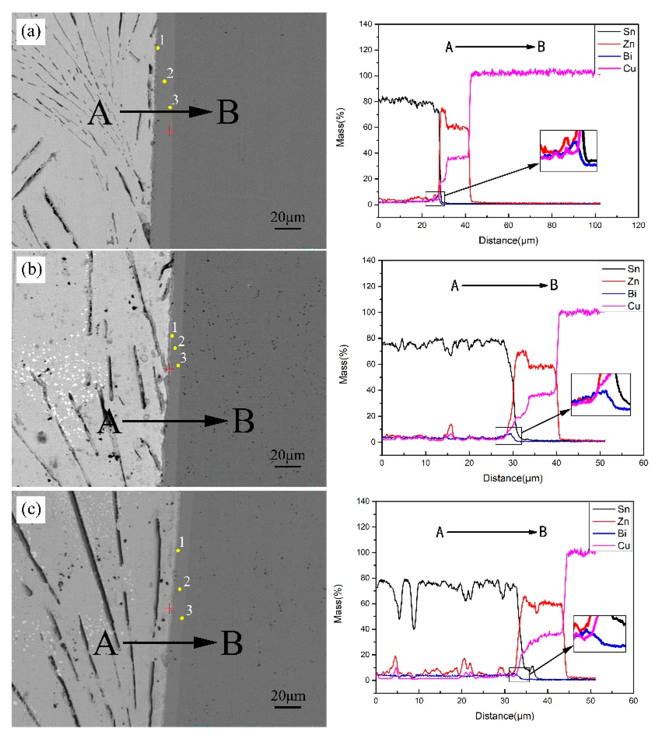
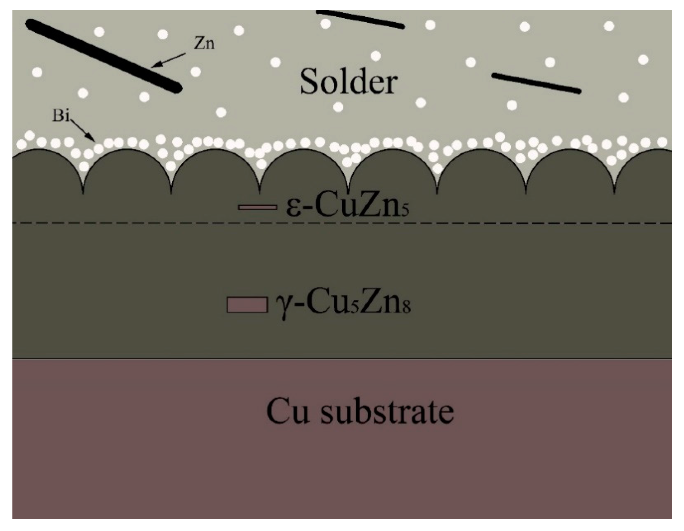
3.6. The Interfacial Reaction in Sn-9Zn-xBi/Cu Joints

Figure 10 and Figure 11 shows the EPMA images and map analyses of the interface of Sn-9Zn-xBi/Cu joints. It can be seen from Figure 10a that small hemisphere-like IMC particles, growing towards the solder matrix, formed at the interface of the Sn-9Zn/Cu solder joint. The elemental distribution maps indicated that the interface in the Sn-9Zn-xBi/Cu solder joint were enriched in Zn and Cu elements. Therefore, it may be confirmed that Cu-Zn IMCs must exist in this IMC layer. When the amount of Bi element is less than 3 wt.%, Bi element cannot be clearly observed on the elemental distribution maps, Bi is uniformly distributed in the solder matrix quite homogeneously. Bi does not react with Sn, Cu, and Zn to form any IMC phases. EPMA point analyses and line analyses across the IMC were also performed and are shown in Figure 12 and Figure 13. From the line scan results of the Sn-9Zn-xBi/Cu joints, It can obviously be found that the concentration of Zn element first increased and then decreased, and the concentration of Cu element gradually increased. Bi element aggregates at the reaction interface, and the IMC showed a serrated morphology. Ladder-shaped line scan curve of the Zn and Cu element shows that the Cu-Zn IMC consisted of two sub-layers. The results of the IMC point analysis (Table 4) also confirmed this prediction. Point analysis location marked as points “1” within the left scallop-like layer, points “2” within the middle layer and points “3” within the right layer. EPMA point analysis showed that the IMC consisted of two layers, and compositions of these two phases are about Zn: Cu = 80:17 and Zn: Cu = 65:35. They are identified to be the ε-CuZn5 closed to the solder and γ-Cu5Zn8 closed to the Cu substrate according to the previous reports. This results are as same as those of Yang’s report [21]. Schematic diagram of IMC layer is showed in Figure 14. From the point analysis and line scan results of Sn-9Zn/Cu joints, the IMC just consisted of γ-Cu5Zn8 layer, indicating that Bi has an impact on the composition of IMC layer. As a small amount of Sn diffused into scallop-like layer and formed an unidentified Cu-Zn-Sn phase, Sn was detected in the scallop-like layer. It is worth noting that during soldering, the Cu-Zn phase was formed instead of Cu-Sn phase. One reason is that Cu-Sn compounds are more difficult to form than Cu-Zn compounds, because Cu-Sn compounds are formed with a higher activation energy [22]. Another reason may be that the Cu-Sn compounds form at a slow rate, so it is not being observed. Therefore, the Cu-Zn compounds is more stable at the IMC layer compared to the Cu-Sn compounds.
Suganuma et al. [23] also conducted related research and reported the existence of three Cu-Zn IMC layers of Sn-9Zn and Cu joints. They are γ-Cu5Zn8 phase, which is close to the solder, and β-CuZn, which is in the middle of the IMC layer, and a thin and unidentified layer close to the Cu substrate. Mayappan et al. [24] reported an IMC layer consisting of ε-CuZn phase and γ-Cu5Zn8 phase. Some studies reported the IMC layer composed of γ-Cu5Zn8 phase [22,25]. The results of these studies are not the same, but they are all Cu-Zn compounds; this is because the composition of the Sn-Zn-based alloy is different, and the reaction temperature is also different.
The whole thickness of the IMC layer was determined by measuring the variation in the distribution of Zn and Cu. The average thicknesses of the IMC layers are listed in Table 5. The thickness of the interfacial reaction layer in Sn-9Zn-2Bi/Cu joints is the maximum, 15.56 μm. When the Bi element content exceeds 3 wt.%, the thickness of the IMC layers decreased. Regarding this phenomenon, the reason is that the Sn-9Zn-xBi solder alloys have lower solidus temperatures. Compared with Sn-9Zn alloy, Sn-9Zn-xBi solder will react with the Cu substrate first, which means that it may experience longer molten periods during the soldering process, leading the thickness of the IMCs to increase. When the IMC was formed, Bi is excluded by the solder, aggregating at the reaction interface, which can be confirmed by the line scan curves. These agminated Bi atoms can reduce the interfacial area of the IMC layer in contact with the molten solder and prevent Zn atoms diffusing into the IMC layer, which causes the formation of the IMC layer to slow down. When the inhibitory effect of aggregated Bi elements on the formation of IMC is greater than the positive effect of a longer reaction time, the thickness of the IMC decreases. The formation of the IMC layer is mainly controlled by a diffusion mechanism.
The thickness of the IMC layers has a direct effect on the joint reliability. An excessively thick IMC may cause micro cracks in the solder joints and decrease the impact ductility. The decreasing of the IMC layer growth can favorably affect the mechanical behavior of the soldered joints. The effect of adding Bi element on the reliability of the joint is expected.

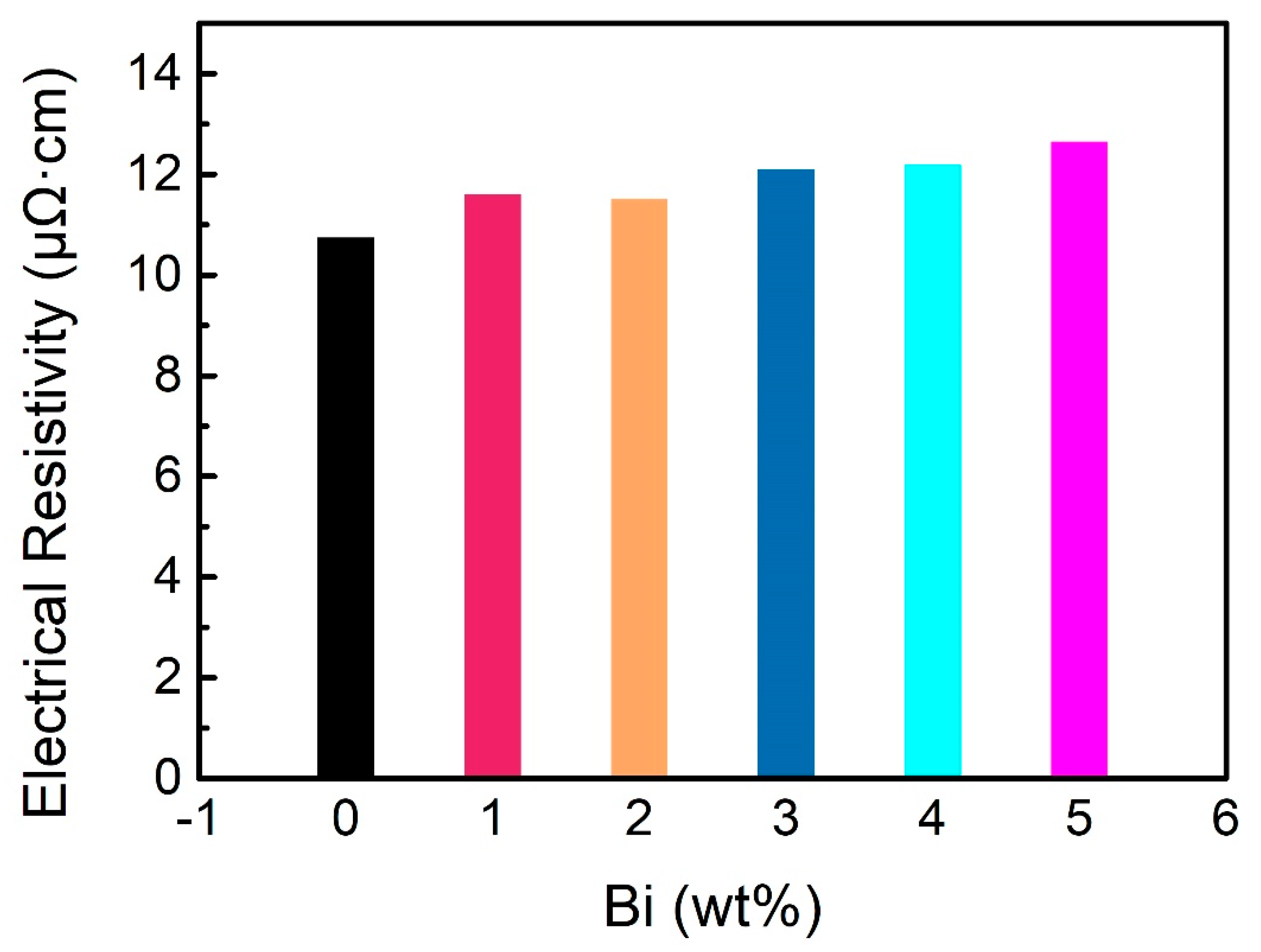
3.7. Electrical Conductivity

The electrical conductivity of the solder is also important because the solder also plays the role of circuit connection on the circuit board. As shown in Figure 15, with the addition of the Bi element the electrical resistivity of Sn-9Zn solders increases, which means the conductivity resistivity decreases. When the addition of Bi increased from 1% to 5%, the electrical resistance increased from 11.627 μΩ·cm to 12.681 μΩ·cm. The formation of a solid solution in solder increases the disorder of the lattice structure. Bi element is dissolved in the alloy, and the original crystal lattice of the solvent is destroyed, which makes the lattice distort and further destroys the periodicity of the lattice potential field. The scattering of electrons increases, leading to an increase in the solder electrical resistivity. When the Bi element content in the solder is over a critical concentration, high-resistivity Bi particles will precipitate from the Sn matrix further. These precipitates act as scattering centers and hinder the motion of electrons, leading to an increase in the solder resistivity. The formation of solid solution and Bi particles in the solder are responsible, mainly, for the increase in the resistivity of the alloy. In addition, the interaction between the alloy components causes a decrease in the number of effective electrons, leading to the increase in the solder resistivity. Moreover, studies have reported that Bi can decrease the number of the Sn4+ state, which results in lesser-charged carriers, leading to an increase in resistivity [26]. The resistivity results shows that there is only a small electrical resistance difference between Sn-9Zn and Sn-9Zn-xBi, therefore the Sn-9Zn-xBi can be taken as a solder joint with an electrical connection role.

4. Conclusions

In this paper, the microstructure, melting behavior, wettability, mechanical behavior, antioxidant properties, and electrical conductivity of Sn-9Zn-xBi alloy, as well as the interfacial reaction in Sn-9Zn-xBi/Cu joints, were investigated. The conclusions garnered from this work are listed below:
(a)
The microstructure of Sn-9Zn-xBi solder alloy consists of a light gray β-Sn matrix, a coarse black acicular Zn-rich phase, and a Sn-Zn eutectic mixture. With the increase in Bi content, the Zn-rich phase disappears at first and then becomes bigger, then white granular Bi precipitates from the Sn matrix.
(b)
The melting temperature, solidus temperature, and liquidus temperature decreased with the increasing Bi addition, but the melting range increased.
(c)
The spreading rate increased and the wetting angle decreased with the increase in Bi content from 1 to 5 wt.%. The addition of Bi obviously improved the wettability of the Sn-9Zn-xBi solder alloy, which can be attributed to the Bi element reducing the surface tension of the molten solder alloy.
(d)
Adding a small amount of Bi can improve the oxidation resistance of the Sn-9Zn solder alloy. However, if the content of Bi is more than 3 wt.%, the oxidation resistance of the Sn-9Zn-xBi alloy will decrease. This is because the Zn-rich phase becomes bigger with an increasing Bi addition, which is harmful to the oxidation resistance.
(e)
Bi atoms would precipitate out from the matrix and produce a lot of brittle particles, which leads to an increase in strength and a significant decrease in plasticity.
(f)
Two reaction layers were formed at the Sn-Zn/Cu interface. They are ε-CuZn5, close to the solder, and γ-Cu5Zn8, closed to the Cu substrate, respectively. The formation of the IMC layer is mainly controlled by a diffusion mechanism.
(g)
The formation of solid solution and Bi particles in the solder alloy, leading to an increase in the scattering of electrons, is mainly responsible for the increase in the resistivity of the alloy.

Author Contributions

Conceptualization, methodology, and writing, Y.Z.P.; original draft preparation, supervision, and resources, C.J.L.; methodology, formal analysis, and investigation, J.J.Y. and J.T.Z.; review and editing, J.B.P., G.J.Z., C.J.P. and J.H.Y. All authors have read and agreed to the published version of the manuscript.

Funding

This work is supported by the Rare and Precious Metal Materials Genome Engineering Project of Yunnan Province (2019ZE001-3, 202002AB080001), the National Natural Science Foundation of China (52061021), and the Young and middle-aged academic and technical leaders reserve talent project (202005AC160039).

Institutional Review Board Statement

Not applicable.

Informed Consent Statement

Not applicable.

Data Availability Statement

Data are available on request.

Conflicts of Interest

The authors declare no conflict of interest.

References

  1. Zhang, L.; Xue, S.-B.; Gao, L.-L.; Sheng, Z.; Ye, H.; Xiao, Z.-X.; Zeng, G.; Chen, Y.; Yu, S.-L. Development of Sn–Zn lead-free solders bearing alloying elements. J. Mater. Sci. Mater. Electron. 2010, 21, 1–15. [Google Scholar] [CrossRef]
  2. Kroupa, A.; Watson, A.; Mucklejohn, S.; Ipser, H.; Dinsdale, A.; Andersson, D. Chapter 5—Lead-free soldering: Environmentally friendly electronics. In Green and Sustainable Manufacturing of Advanced Material; Singh, M., Ohji, T., Asthana, R., Eds.; Elsevier: Oxford, UK, 2016; pp. 101–134. [Google Scholar] [CrossRef]
  3. Cheng, S.; Huang, C.-M.; Pecht, M. A review of lead-free solders for electronics applications. Microelectron. Reliab. 2017, 75, 77–95. [Google Scholar] [CrossRef]
  4. Kotadia, H.R.; Howes, P.D.; Mannan, S.H. A review: On the development of low melting temperature Pb-free solders. Microelectron. Reliab. 2014, 54, 1253–1273. [Google Scholar] [CrossRef]
  5. Xu, J.; Xue, S.; Xue, P.; Long, W.-M.; Zhang, Q.-K. Study on microstructure and properties of Sn–0.3Ag–0.7Cu solder bearing Nd. J. Mater. Sci. Mater. Electron. 2016, 27, 8771–8777. [Google Scholar] [CrossRef]
  6. Bieler, T.R.; Lee, T.-K. Lead-free solder. In Encyclopedia of Materials: Science and Technology; Buschow, K.H.J., Cahn, R.W., Flemings, M.C., Ilschner, B., Kramer, E.J., Mahajan, S., Veyssière, P., Eds.; Elsevier: Oxford, UK, 2010; pp. 1–12. [Google Scholar] [CrossRef]
  7. Liu, J.-C.; Zhang, G.; Ma, J.-S.; Suganuma, K. Ti addition to enhance corrosion resistance of Sn–Zn solder alloy by tailoring microstructure. J. Alloys Compd. 2015, 644, 113–118. [Google Scholar] [CrossRef]
  8. Islam, R.A.; Chan, Y.C.; Jillek, W.; Islam, S. Comparative study of wetting behavior and mechanical properties (microhardness) of Sn–Zn and Sn–Pb solders. Microelectron. J. 2006, 37, 705–713. [Google Scholar] [CrossRef]
  9. Zhou, J.; Sun, Y.; Xue, F. Properties of low melting point Sn–Zn–Bi solders. J. Alloys Compd. 2005, 397, 260–264. [Google Scholar] [CrossRef]
  10. Chen, W.X.; Xue, S.B.; Wang, H.; Wang, J.X.; Han, Z.J.; Gao, L.L. Effects of Ag on microstructures, wettabilities of Sn–9Zn–xAg solders as well as mechanical properties of soldered joints. J. Mater. Sci. Mater. Electron. 2010, 21, 461–467. [Google Scholar] [CrossRef]
  11. Xue, P.; Xue, S.-B.; Shen, Y.-F.; Zhu, H.; Gao, L.L. Study on properties of Sn-9Zn-Ga solder bearing Nd. J. Mater. Sci. Mater. Electron. 2012, 23, 1272–1278. [Google Scholar] [CrossRef]
  12. Zhou, J.; Huang, D.; Fang, Y.-L.; Xue, F. Investigation on properties of Sn-8Zn-3Bi lead-free solder by Nd addition. J. Alloys Compd. 2009, 480, 903–907. [Google Scholar] [CrossRef]
  13. Mahdavifard, M.H.; Sabri, M.F.M.; Shnawah, D.A.; Said, S.M.; Badruddin, I.A.; Rozali, S. The effect of iron and bismuth addition on the microstructural, mechanical, and thermal properties of Sn-1Ag-0.5Cu solder alloy. Microelectron. Reliab. 2015, 55, 1886–1890. [Google Scholar] [CrossRef]
  14. Eid, E.A.; El-Khawas, E.H.; Abd-Elrahman, A.S. Impact of Sb additives on solidification performance, microstructure enhancement and tensile characteristics of Sn-6.5Zn-0.3Cu Pb-free solder alloy. J. Mater. Sci. Mater. Electron. 2019, 30, 6507–6518. [Google Scholar] [CrossRef]
  15. Hu, X.; Li, Y.; Liu, Y.; Min, Z. Developments of high strength Bi-containing Sn0.7Cu lead-free solder alloys prepared by directional solidification. J. Alloys Compd. 2015, 625, 241–250. [Google Scholar] [CrossRef]
  16. El-Daly, A.A.; Hashem, H.A.; Radwan, N.; El-Tantawy, F.; Dalloul, T.R.; Mansour, N.A.; Abd-Elmoniem, H.M.; Lotfy, E.H. Robust effects of Bi doping on microstructure development and mechanical properties of hypoeutectic Sn–6.5Zn solder alloy. J. Mater. Sci. Mater. Electron. 2016, 27, 2950–2962. [Google Scholar] [CrossRef]
  17. Zhao, G.-J.; Wen, G.-H.; Sheng, G.-M. Influence of rapid solidification on Sn-8Zn-3Bi alloy characteristics and microstructural evolution of solder/Cu joints during elevated temperature aging. Trans. Nonferrous Met. Soc. China 2017, 27, 234–240. [Google Scholar] [CrossRef]
  18. Moon, K.-W.; Boettinger, W.J.; Kattner, U.R.; Handwerker, C.A.; Lee, D.-J. The effect of Pb contamination on the solidification behavior of Sn-Bi solders. J. Electron. Mater. 2001, 30, 45–52. [Google Scholar] [CrossRef]
  19. Erer, A.M.; Oguz, S.; Türen, Y. Influence of bismuth (Bi) addition on wetting characteristics of Sn-3Ag-0.5Cu solder alloy on Cu substrate. Eng. Sci. Technol. Int. J. 2018, 21, 1159–1163. [Google Scholar] [CrossRef]
  20. Jiang, J.; Lee, J.-E.; Kim, K.-S.; Suganuma, K. Oxidation behavior of Sn–Zn solders under high-temperature and high-humidity conditions. J. Alloys Compd. 2008, 462, 244–251. [Google Scholar] [CrossRef]
  21. Yang, C.-F.; Chen, S.-W.; Wu, K.-H.; Chin, T.-S. Interfacial reactions of Sn-8wt.%Zn-3wt.%Bi solder with Cu, Ag, and Ni substrates. J. Electron. Mater. 2007, 36, 1524–1530. [Google Scholar] [CrossRef]
  22. Liu, J.; Zhou, W.; Liu, L.; Wu, P. Cu5Zn8 growth reversion in Cu/Sn-8Zn-3Bi/Cu during discontinuous electromigration. J. Electron. Mater. 2012, 41, 2045–2050. [Google Scholar] [CrossRef]
  23. Suganuma, K.; Niihara, K.; Shoutoku, T.; Nakamura, Y. Wetting and interface microstructure between Sn–Zn binary alloys and Cu. J. Mater. Res. 1998, 13, 2859–2865. [Google Scholar] [CrossRef]
  24. Mayappan, R.; Ismail, A.B.; Ahmad, Z.A.; Ariga, T.; Hussain, L.B. The effect of crosshead speed on the joint strength between Sn-Zn-Bi lead-free solders and Cu substrate. J. Alloys Compd. 2007, 436, 112–117. [Google Scholar] [CrossRef]
  25. Kim, D.-G.; Jang, H.-S.; Jung, S.-B. Solid state intermetallic compound layer growth between Sn-8Zn-3Bi solder and bare copper substrate. J. Mater. Sci. Mater. Electron. 2005, 16, 523–528. [Google Scholar] [CrossRef]
  26. Jaffery, H.A.; Mohd Sabri, M.F.; Rozali, S.; Mahdavifard, M.H.; Shnawah, D.A. Effect of temperature and alloying elements (Fe and Bi) on the electrical resistivity of Sn-0.7Cu solder alloy. RSC Adv. 2016, 6, 58010–58019. [Google Scholar] [CrossRef]
Figure 1. Schematic diagram of the wetting test process.
Metals 11 00538 g001
Figure 2. Back-scattered electron (BSE) images of Sn-9Zn-xBi solder alloys: (a) Sn-9Zn; (b) S n-9Zn-1Bi; (c) Sn-9Zn-2Bi; (d) Sn-9Zn-3Bi; (e) Sn-9Zn-4Bi; (f) Sn-9Zn-5Bi.
Metals 11 00538 g002
Figure 3. EPMA images and map analyses of the interface of Sn-9Zn-3Bi: (a) BSE images; (b) Sn element; (c) Zn element; (d) Bi element.
Metals 11 00538 g003
Figure 4. EPMA images and map analyses of the interface of Sn-9Zn-5Bi: (a) BSE images; (b) Sn element; (c) Zn element; (d) Bi element.
Metals 11 00538 g004
Figure 5. DSC curves of the solder alloys: (a) Sn-9Zn; (b) S n-9Zn-1Bi; (c) Sn-9Zn-2Bi; (d) Sn-9Zn-3Bi; (e) Sn-9Zn-4Bi; (f) Sn-9Zn-5Bi.
Metals 11 00538 g005
Figure 6. Spreading rate of the Sn-9Zn-xBi solder alloys on the Cu substrate.
Metals 11 00538 g006
Figure 7. Contact angle image of Sn-9Zn-xBi alloy: (a) x = 1; (b) x = 2; (c) x = 3; (d) x = 4; (e) x = 5.
Metals 11 00538 g007
Figure 8. The thermal gravimetric analysis curve of Sn-9Zn-xBi alloys.
Metals 11 00538 g008
Figure 9. Engineering stress–strain curves of Sn-9Zn-xBi alloys.
Metals 11 00538 g009
Figure 10. EPMA images and map analyses of the interface of Sn-9Zn-xBi/Cu joints: (a) x = 0; (b) x = 1; (c) x = 2.
Metals 11 00538 g010
Figure 11. EPMA images and map analyses of the interface of Sn-9Zn-xBi/Cu joints: (a) x = 3; (b) x = 4; (c) x = 5.
Metals 11 00538 g011
Figure 12. EPMA images and line analyses of the interface of Sn-9Zn-xBi/Cu joints: (a) x = 0; (b) x = 1; (c) x = 2.
Metals 11 00538 g012
Figure 13. EPMA images and line analyses of the interface of Sn-9Zn-xBi/Cu joints: (a) x = 3; (b) x = 4; (c) x = 5.
Metals 11 00538 g013
Figure 14. Schematic diagram of cross-sections of IMC layer formed in Sn-9Zn-xBi/Cu solder joint.
Metals 11 00538 g014
Figure 15. Electrical resistivity of the Sn-9Zn-xBi solder alloys.
Metals 11 00538 g015
Table 1. Chemical composition of the Sn-Zn-xBi alloys analyzed by inductively coupled plasma (ICP) analysis.
AlloyZn(wt.%)Bi(wt.%)Sn(wt.%)
Sn-9Zn9.03090.97
Sn-9Zn-1Bi9.141.0189.85
Sn-9Zn-2Bi8.882.0289.10
Sn-9Zn-3Bi8.763.0188.23
Sn-9Zn-4Bi8.913.9887.11
Sn-9Zn-5Bi8.854.8786.28
Table 2. DSC results for various solder alloys.
AlloyTonset (°C)Toffset (°C)Tm (°C)Pasty Range (°C)Enthalpy (J/g)
Sn-9Zn198.62202.93199.894.3186.45
Sn-9Zn-1Bi197.01200.62198.373.6184.56
Sn-9Zn-2Bi195.41199.45197.394.0482.82
Sn-9Zn-3Bi193.89198.30196.484.4180.18
Sn-9Zn-4Bi192.65197.32195.564.6779.76
Sn-9Zn-5Bi191.33196.32194.674.9977.59
Table 3. Tensile strength and elongation of Sn-9Zn-xBi alloys.
Alloyσ/MPaδ/%
Sn-9Zn6117.5
Sn-9Zn-1Bi6825.0
Sn-9Zn-2Bi7922.5
Sn-9Zn-3Bi8420.0
Sn-9Zn-4Bi9812.5
Sn-9Zn-5Bi1077.5
Table 4. Point analysis results of the IMCs, as shown in Figure 10.
AlloyLocationComposition (Mol%)
ZnCuSnBi
Sn-9Zn164.3932.52.110
264.0735.5600
363.0136.640.350
Sn-9Zn-1Bi180.5517.282.140.03
264.9834.640.360.02
363.8035.880.310.01
Sn-9Zn-2Bi178.5017.224.240.04
265.0134.340.650
363.7135.780.460.05
Sn-9Zn-3Bi180.9317.941.120.01
264.4335.070.480.01
363.6035.980.420
Sn-9Zn-4Bi179.0318.432.500.05
263.4935.481.030
362.4136.700.860.03
Sn-9Zn-5Bi177.2218.574.170.03
265.8633.600.540
364.3535.190.430.03
Table 5. Average thickness of the IMC layer after soldering.
AlloysSn-9ZnSn-9Zn-1BiSn-9Zn-2BiSn-9Zn-3BiSn-9Zn-4BiSn-9Zn-5Bi
thickness (μm)14.0314.8815.9013.3711.8511.61
14.7615.1415.3913.6211.6011.59
14.3013.8815.3913.8712.1511.61
Average (μm)14.3614.6315.5613.6211.8711.60
Publisher’s Note: MDPI stays neutral with regard to jurisdictional claims in published maps and institutional affiliations.

