Article

Plasmonic Gold Nanorod Size-Controlled: Optical, Morphological, and Electrical Properties of Efficiency Improved Tin Disulfide Vacuum-Free Hybrid Solar Cells

School of Chemical Engineering, Yeungnam University, 280 Daehak-Ro, Gyeongsan 38541, Korea
*
Authors to whom correspondence should be addressed.
Metals 2021, 11(12), 1911; https://doi.org/10.3390/met11121911
Submission received: 26 October 2021 / Revised: 22 November 2021 / Accepted: 24 November 2021 / Published: 26 November 2021

Abstract

:
The different size of plasmonic gold nanorods (NRs) were synthesized by the overgrown seeds method and applied to vacuum-free hybrid solar cells (VFHSCs). Tin disulfide (SnS2) quantum dots were synthesized and used as an n-type material of the device. The synthesized materials were characterized by different techniques such as transmission electron microscopy (TEM), UV-Vis spectroscopy, and atomic force microscopy (AFM). The Au (NRs) had a different of size of NR1 (Width: 4 nm; Length: 12 nm), NR2 (Width: 5 nm; Length: 16 nm), NR3 (Width: 6 nm; Length: 22 nm) which were measured using a TEM technique. The Au NR particles were incorporated into the PEDOT:PSS as a hole transport layer (HTL) of solar cells device. The effects of Au NRs size on the device performance were investigated. A thin film of Zin oxide (ZnO) was used as a buffer layer of the device. The influence of buffer layer thickness on the device’s active layer surface morphology was also studied. At the optimized condition, the highest power conversion efficiency was obtained at about ~3.7%.

1. Introduction

Quantum dots (Qdots) solar cells have garnered great interest in the field of inorganic solar cells in the last decade because of their nontoxic, simple processing, low-temperature fabrication, low cost, and abundant materials in the earth [1,2]. Tin disulfide (SnS2) quantum dots are a semiconductor with a bandgap energy of about ~2.2 eV [3]. Many research groups have studied of SnS2 as n-type material blending with an organic polymer for hybrid solar cells [4,5]. However, the power conversion efficiency (PCE) was still low because of many effects, including that SnS2 particles are not well dispersed, as well as their particle size. The dispersion and high crystalline SnS2 Q-dots particle are the most important factors to form an interpenetrating electron pathway in the hybrid solar cells (HSCs).
There are many ideas to enhance the power conversion efficiency of SnS2 devices, such as the optimization of active layer surface morphology, controlling the size of SnS2 nanoparticles, and improving of the slight absorption using a different narrow bandgap polymer as a donor material [6,7,8]. A large number of low bandgap polymers were applied as light absorption materials, including Alternating poly fluorine copolymer (APFO-3), Benzodipyrrolidone-benzene (PBDPDP-B), benzodipyrrolidione-thiophene (PBDPD-T), and Poly[[4,8-bis[(2-ethylhexyl)oxy]benzo[1,2-b:4,5-b’]dithiophene-2,6-diyl][3-fluoro-2-[(2-ethylhexyl)carbonyl]thieno[3,4b]thiophenediyl]] (PTB7).
There are a lot of improvements in device structure and material that have been investigated so far, but the PCE of VFHSCs remains low compared with the organic solar cells. The thickness of the photoactive film in an VFHSCs device is limited to a few hundred nanometers because of the short electron interpenetration pathway and the exciton diffusion length of inorganic materials. The light absorption limitation led to the lowing of device efficiency.
For this reason, the enhancement of light absorption is an important research activity in the solar cells field. Therefore, the optical properties such as absorption and scattering depend on the electromagnetic field strength and optical path length. The total light absorption might be increased without increasing the photoactive layer thickness by incorporating the plasmonic nanostructure. Several researcher groups have investigated the use of metallic plasmonic nanostructures to improve the performance of the solar cells [9,10,11,12], by adding of metal nanoparticles into the photoactive layer or hole transport layer, or both.
In this paper, gold plasmonic nanorods with different sizes were synthesized and added to the hole transporting layer of the VFHSC device. The effects of Au NR on the optical, morphological, and electrical properties of the device were investigated. With Au NR2 (W: 5 nm; L: 16 nm), a maximum efficiency increased from 1.5% to 2.8%) was demonstrated. To improve the device performance, the photoactive layer’s surface morphology was well controlled by depositing a thin layer of zin oxide (ZnO). Henceforth, at the optimized condition, the device performance was improved.

2. Materials and Methods

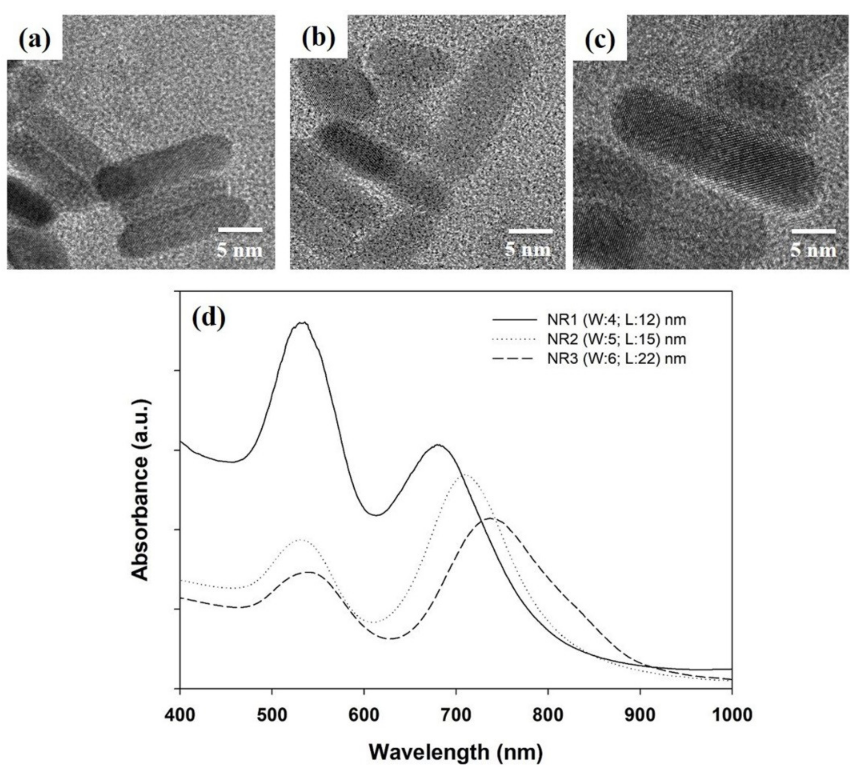
2.1. Preparation of Au Nanorods

The plasmonic Au NRs were prepared by modifying the seed-mediated methods [13,14]. The solution of CTAB (9.75 mL, 0.01 M) was injected to the solution of 0.01 M AgNO3 at 27 °C. Then, 0.5 mL of 0.01 M HAuCl4 was injected. After that, 80 μL of 0.1 M ascorbic acid was then added into the solution. Finally, 20 μL of seed solution of CTAB (9.75 mL, 0.1 M) was injected and kept stirred for more than 10 h at a temperature of 30 °C. The impurities were removed using the centrifugation technique with different speeds, and then the Au NRs were dispersed in DI water.

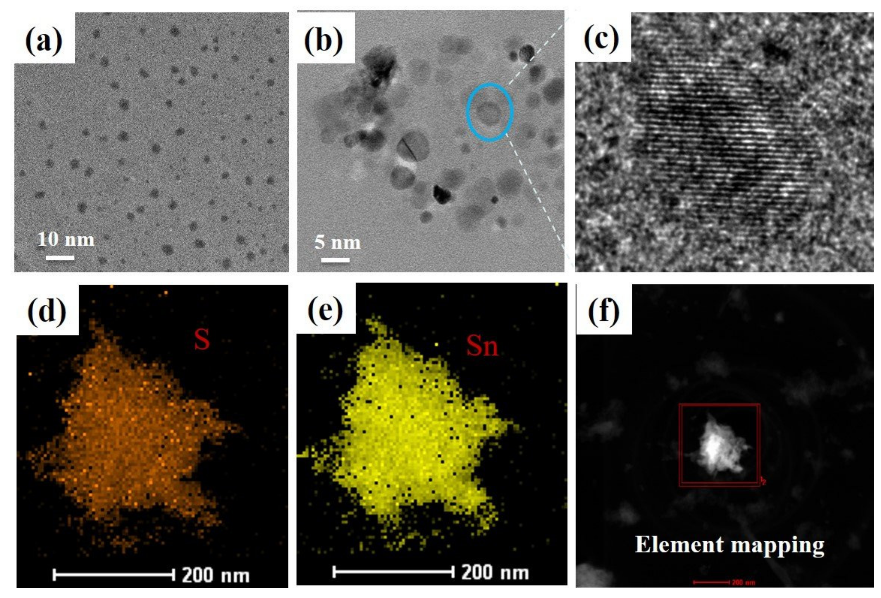
2.2. Preparation of SnS2 Quantum Dots Nanoparticles

SnS2 quantum dots were prepared by using a modified wet synthesis method [15]. In detail, the mixture of anhydrous tin (IV) chloride (0.1 mL) with oleylamine (20 mL) was heated at 120 °C for 30 min, and then the solution was heated up to 200 °C. The mixture of oleyamine (3 mL) and thioacetamide (0.22 mg) was added at this temperature and kept at 200 °C for 12 h under a nitrogen environment. Then, the solution was cooled down to room temperature. The final solution was washed several times with ethanol using the centrifuge technique. The final product was dried at 90 °C for more than 24 h in a dry box.

2.3. Preparation of (PEDOT:PSS + Au Nrods) Thin Film

The (PEDOT:PSS + Au NRs) solution was prepared by mixing of 5 mL Au nanorods solutions and 100 mL of PEDOT:PSS and stirred more than 24 h. Before coating on the cleaned-glass/ITO, the solution was sonicated for 1 h at room temperature.

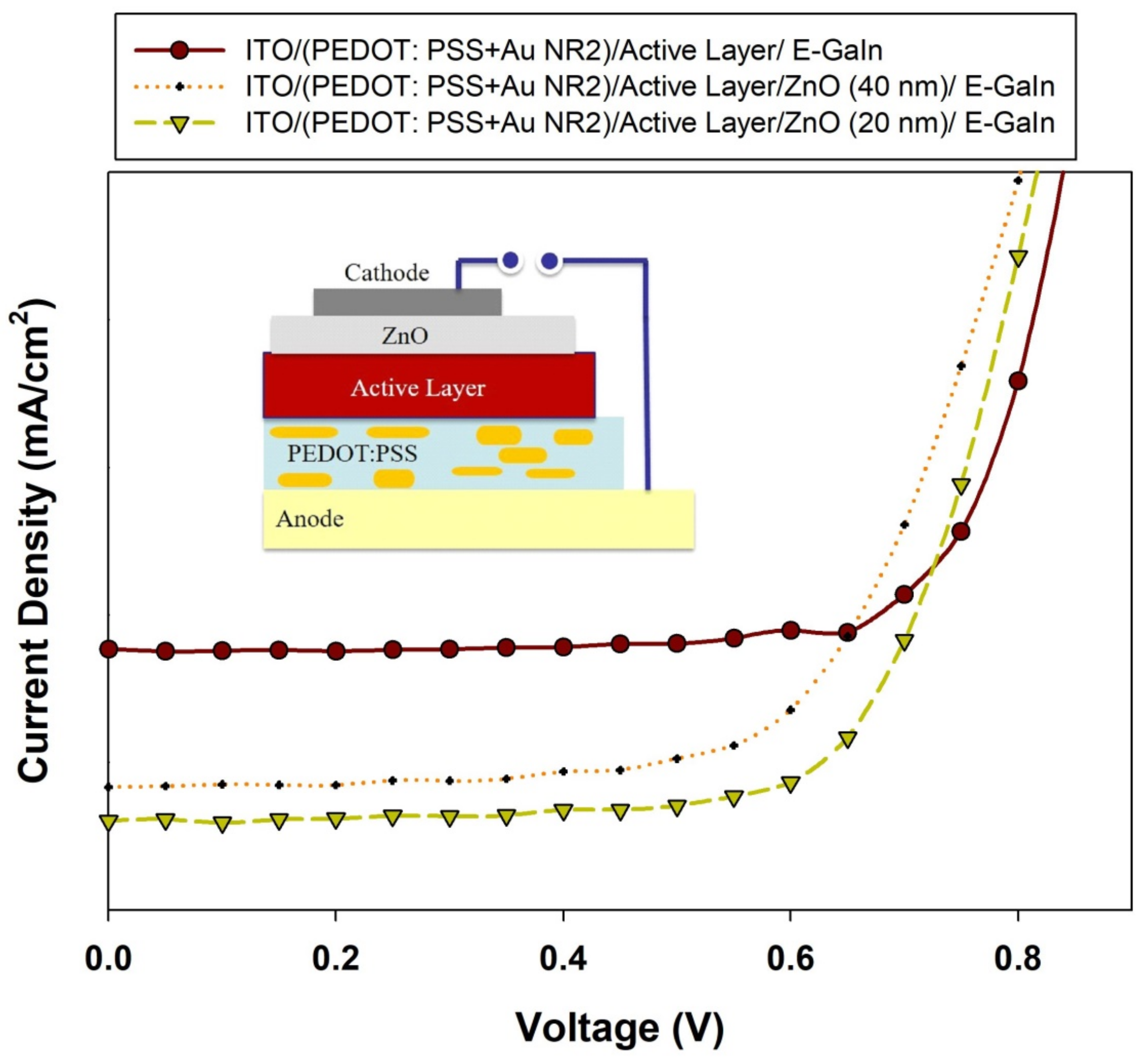
2.4. Device Fabrication

ITO coated glass substrate was cleaned with methanol and acetone using ultrasonic for 20 min of each. Then the solution of (Au NRs+ PEDOT:PSS) was spin-coated on the Glass/ITO at a speed of 4000 rounds per minute (rpm) for 60 s and dried at 100 °C for 1 h under nitrogen environment by vacuum oven. A solution of (SnS2 + PBT7) in binary solvent as chlorobenzene/chloroform was prepared and stirred overnight to form a composite solution. This solution was deposited on the Glass/ITO/(Au NRs+ PEDOT:PSS) at 3000 rpm for 60 s and dried at 140 °C for 20 min. After that, the ZnO layer was deposited with different of speed for 40 s and dried at 120 °C for 20 min. Finally, the cathode layer of E-GaIn was coated to complete the device structure of the Glass/ITO/(Au NRs+ PEDOT:PSS)/(SnS2 + PTB7)/ZnO/E-GaIn.

2.5. Characterization

The morphology and absorption properties of (SnS2, Au NRs) were analyzed using a transmission electron microscope (TEM), high-resolution TEM (HR-TEM), and ultraviolet-visible (UV-vis). The surface morphology and topography morphology (RMS) were measured using scanning electron microscope (SEM), video contact angle (VCA), and the atomic force microscopy (AFM) technique. The device’s parameters such as (FF) Fill factor (%), (Jsc) short circuit current density (mA/cm2), (Voc) open circuit voltaic (V), and (PCE) power conversion efficiency (%) were measured using solar simulator (Keithley 69911, Beaverton, OR, USA) under AM 1.5 illumination at 100 mW/cm2.

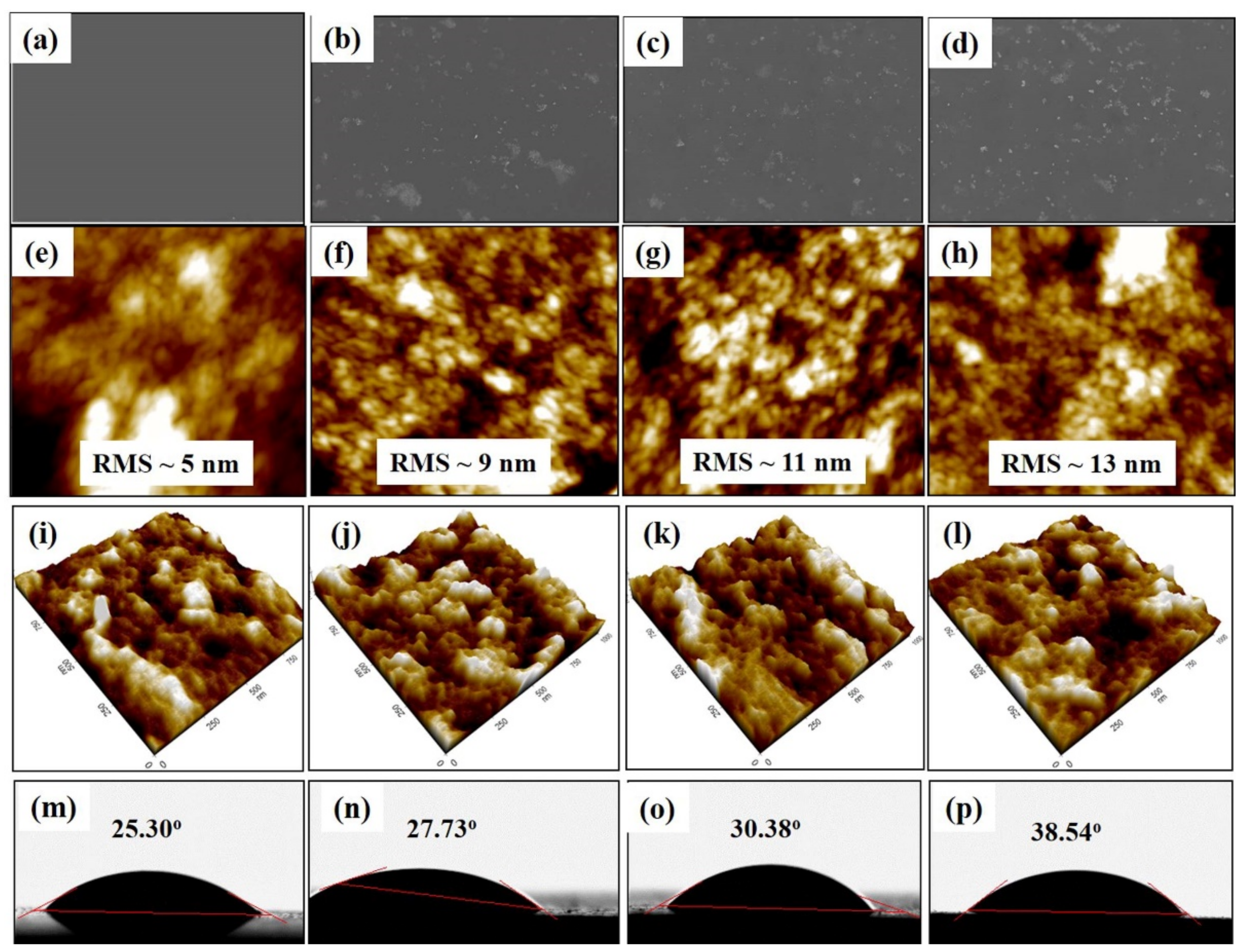
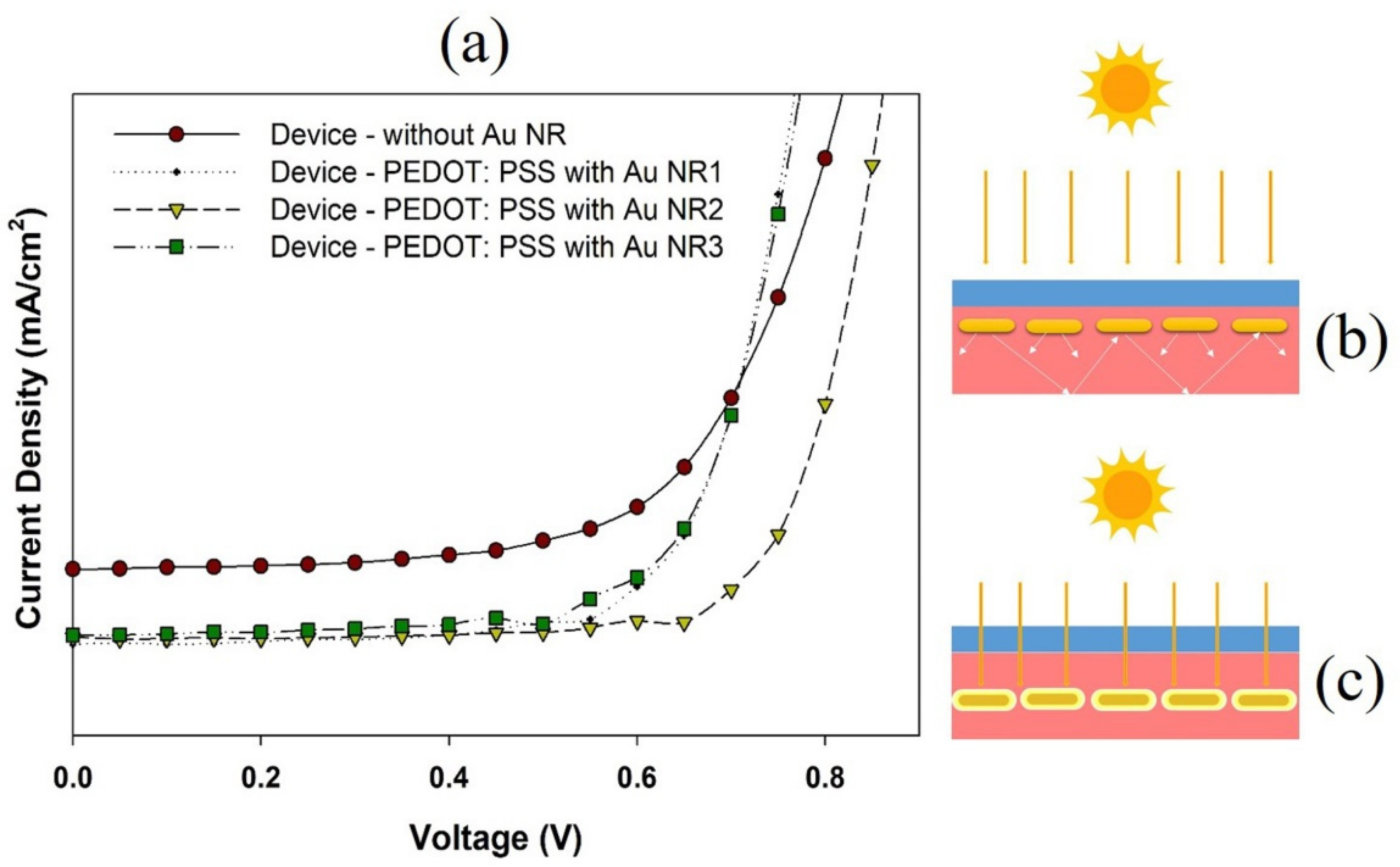
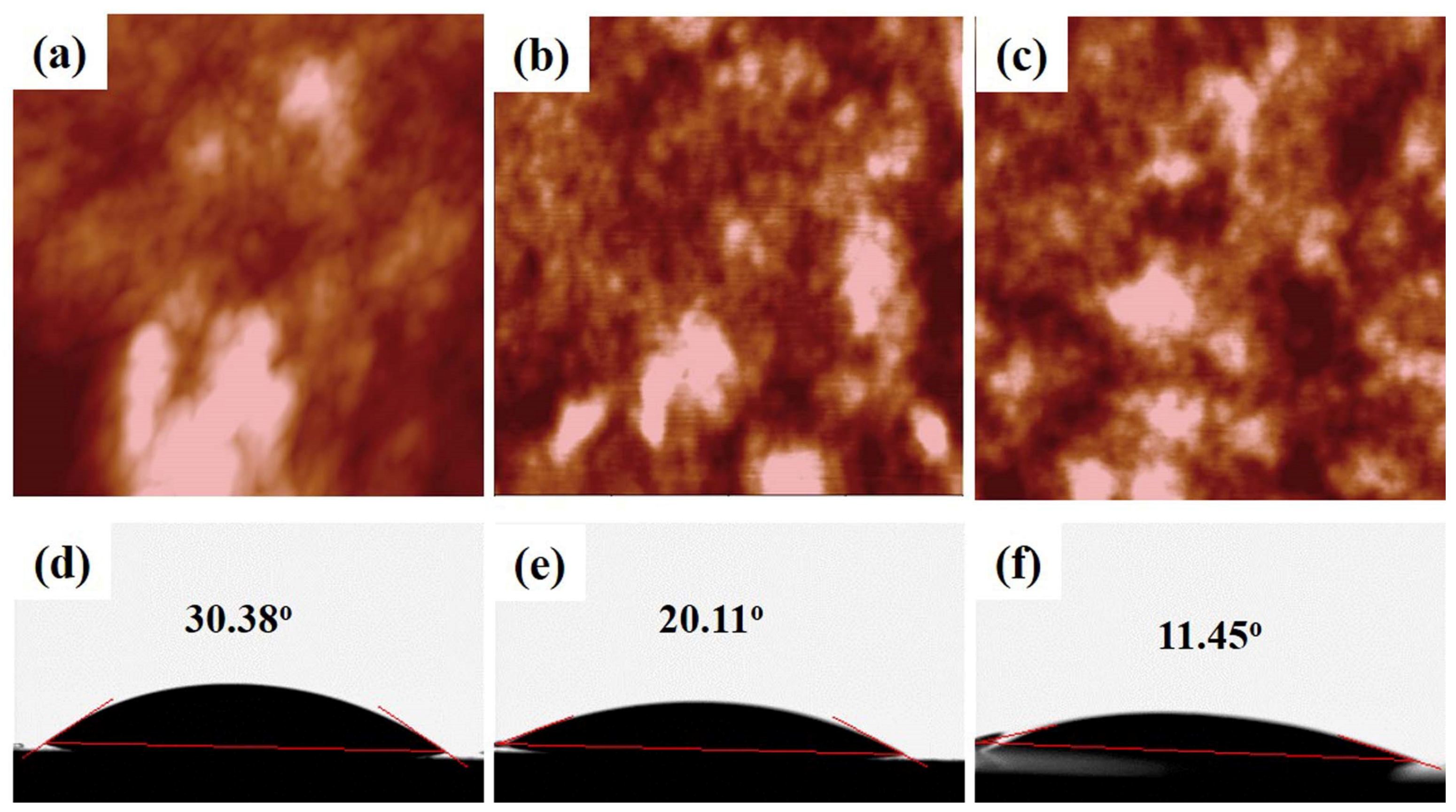
3. Results and Discussion

Figure 1a,b shows TEM images of the SnS2 NPs, which have a size in the range of 3–10 nm. Figure 1c presents the HR-TEM image in which the lattice fringes are very clearly visible, confirming that the SnS2 NPs obtained in this study are very highly crystalline [6]. Figure 1d–f further shows the elemental mapping of nanostructures reveals well uniform of SnS2 nanocrystals structure. The optical and structural properties were also investigated [15]. The absorption spectrum in the wavelength range of 350–450 nm and the crystal structure of SnS2 NPs was investigated using the X-ray diffraction (XRD) technique, which showed that the SnS2 NPs had a hexagonal structure with crystal planes of (002) (100) (110) and (200) corresponding to the peaks of 17, 30, 51, and 60° in the previous work [15]. The high-resolution TEM images and XRD crystal planes clearly show that the phase of SnS2 NPs was very highly crystalline with hexagonal phase structure.
Figure 2 shows the morphology and absorption spectrum of gold nanorods with different size. Figure 2a–c shows the Au NRs with different sizes, which was measured by TEM technique. There are three types of gold NR particles with the size of NR1 (W:4; L:12) nm, NR2 (W:5; L:15) nm, and NR3 (W:4; L:12) nm. Figure 2d shows the absorption spectrums of Au nanorods with different sizes, which presents two absorption bands in the range of 500–700 nm. Two absorption peaks confirmed two characteristic peaks of Au NRs. When the size of Au NRs is increased, the absorption band is shifted to a longer wavelength.
The surface roughness of PEDOT:PSS layer without and with Au NRs with different of size were investigated, as shown in Figure 3. Figure 3a–d presents the SEM images of surface morphology, which shows that the PEDOT:PSS film without Au NRs (Figure 3a) presents high uniformity of morphology. However, the PEDOT:PSS film with Au NRs (Figure 3b–d) depicts that the morphology of the film became rougher with some pinholes appearing. The surface roughness of all samples was studied using the AFM technique, as shown in Figure 3e–l. The without Au NRs film shows that the surface roughness is about ~5 nm, while the sample with Au NR1, Au NR2, and Au NR3 have a roughness of 9.2 nm, 11.4 nm, and 13.2 nm, respectively. Figure 3m–p presents the contact angle images of the PEDOT:PSS with and without Au NRs. Without Au NRs, the thin film shows that the contact angle is about ~25.30°, while the films with Au NR1, Au NR2, and Au NR3 have a contact angle of 27.73, 30.38, and 38.54°, respectively. When the size of Au increases, the surface roughness also increases.
The effects of Au nanorods on the electrical properties of the device were studied with the sample cell’s structure of ITO/(Au NRs + PEDOT:PSS)/(PTB7 + SnS2)/E-GaIn. The I-V curves from Figure 4a and Table 1 depict the device’s parameters. The device without Au shows the lowest efficiency of about ~1.5% (Jsc: 3.4 mA/cm2), while the devices with Au NR1, Au NR2, and Au NR3 show an efficiency of ~2.3% (Jsc: 4.4 mA/cm2), 2.8% (Jsc: 4.47 mA/cm2), and 2.1% (Jsc: 4.3 mA/cm2), respectively. The obtained result shows that, by adding the Au nanorods with different sizes into the buffer layer, the device’s efficiencies are increased.
When plasmon Au NRs are incorporated into the buffer layer of the HVFSC solar cell device, the improvement of absorption may be achieved by two mechanisms. The first mechanism is the scattering effect, which strengthens the metal nanoparticles. Improving the scattering at the front surface of a solar cell device reduces the Fresnel reflection, leading to an optical path length much longer than the thickness of the absorption film [16], as shown in Figure 4b. The second mechanism is the local field enhancement effect of surface plasmons, which are highly effective in concentrating electric field at the interface of the Au NRs and the dielectric material. A resonance might be obtained while tuning the excitation light when the frequency of the incident light is equal to the collective oscillation frequency of the free electron of the Au NRs [17], as shown in Figure 4c. Both mechanisms strongly depend on the size and sharpness of Au NRs. Since the Au NRs incorporated in the PEDOT:PSS film are not in contact directly with the photoactive layer. The main reason for improving light-harvesting might be by the forward scattering of the income sunlight and this is the main mechanism of the power conversion efficiency enhancement when the Au NRs are incorporated in PEDOT:PSS. The absorption and scattering property of the metal nanoparticles is strongly dependent on their size and sharpness, which have been well investigated [18,19]. Researchers have reported the same wavelength dependence for the extinction (including absorption and scattering) of small the size Au nanoparticles. In the case of big-size Au nanoparticles, the scattering is enhanced, relative to the increase of the absorption in the longer wavelength visible region of the spectrum. Enhancing the scattering and absorption leads to the increase of charge transport in the photoactive layer, which leads to an increase in the hole collection efficiency at the back contact, and thus improves the short circuit current and efficiency.
To improve the device’s efficiency, the Au NR2 incorporated device’s active layer morphology should be controlled to improve the morphology of the interface between the active layer and cathode. The ZnO film was deposited at the interface between the active layer and cathode. The ZnO film was used as an electron transport layer to help electron transport from the p-n junction interface to the electrode and also was used to improve the surface morphology of the device active layer. In Figure 5a–c, the surface roughness of the photoactive layer with different the thickness of ZnO film was confirmed. In the case without ZnO film, the photoactive layer surface roughness was about ~11 nm, while in the case of the sample with ZnO (T ~ 40 nm) and ZnO (T ~ 20 nm), the photoactive layer surface roughness showed ~7 nm and ~5 nm, respectively.
A small droplet of water was placed on the thin film’ surface and the contact angle between the water droplet edge and the film was measured. A smaller contact angle signifies higher film energy and that the surface of film is hydrophilic, and it becomes more hydrophilic when the surface roughness is smoother.
Figure 5d–f presents the contact angle of the photoactive layer morphology with and without ZnO layer coating. Without the ZnO layer shows a contact angle of about ~32.51°, while the films with ZnO (T ~ 40 nm) and ZnO (T ~ 20 nm) show a contact angle of 20.21 and 11.45°, respectively. The obtained result shows that adding the ZnO leading to the photoactive surface morphology was improved, causing the enhancement of the device performance.
The effects of the ZnO layer on the electrical property of device performance were studied by fabricating solar cells with the structure of ITO/(PEDOT:PSS + Au NR2)/(PTB7 + SnS2)/ZnO/E-GaIn, as shown in Figure 6 and Table 2. The I-V curve of the device without Au shows an efficiency of about ~2.8% (Jsc: 4.47 mA/cm2), while the devices with ZnO (T ~ 40 nm) and ZnO (T ~ 20 nm) show an efficiency of ~3.1% (Jsc: 6.3 mA/cm2) and 3.7% (Jsc: 6.8 mA/cm2), respectively. The improvement of device efficiency is possible to explain by enhancement of the surface roughness and morphology of the photoactive layer, which led to improvement in the interface between the photoactive layer and the back contact of E-GaIn.

4. Conclusions

Gold nanoparticles with different sizes were controlled and incorporated into the PEDOT:PSS layer of the tin disulfide/polymer vacuum-free hybrid solar cells. The scattering effect of Au NRs with different sizes was investigated to enhance the optical properties of the device such as light scattering, light-harvesting, and the charge carrier’s transport in the device structure which leads to the enhancement in the device performance. The device efficiency was increased by coating of ZnO (~20 nm) film to enhance the active layer surface morphology, which led to enhancing the contact between (SnS2 + PTB7) and E-GaIn back contact. The highest cells efficiency is about ~3.7% (Jsc = 6.8 mA/cm2; Voc = 0.75 (V); FF = 70) for the cell with structure of Glass/ITO/(Au NR2 + PEDOT:PSS)/(SnS2 + PTB7)/ZnO (20 nm)/E-GaIn.

Author Contributions

Writing—original draft, Conceptualization, Methodology, Data interpretation, M.K. and N.T.N.T.; Data curation Validation, Resources N.H.L. and N.L.; Visualization, Formal analysis, A.M.T. Writing—review & editing, M.S.T.; Supervision, Project administration. Funding acquisition, J.H.J. All authors have read and agreed to the published version of the manuscript.

Funding

This work was supported by the 2016 Yeungnam University Research Grant.

Institutional Review Board Statement

Not applicable.

Informed Consent Statement

Not applicable.

Data Availability Statement

Not applicable.

Conflicts of Interest

The authors declare that they have no known competing financial interest or personal relationships that could appear to influence the work reported in this paper.

References

  1. Watt, A.A.; Blake, D.; Warner, J.H.; Thomsen, E.A.; Tavenner, E.L.; Dunlop, H.R.; Meredith, P. Lead sulfide nanocrystal: Conducting polymer solar cells. J. Phys. D 2005, 38, 2006. [Google Scholar] [CrossRef] [Green Version]
  2. Zeng, T.W.; Lin, Y.Y.; Lo, H.H.; Chen, C.W.; Liu, S.C.; Huang, H.Y.; Su, W.F. A large interconnecting network within hybrid MEH-PPV/TiO2 nanorod photovoltaic devices. Nanotechnology 2006, 17, 5387. [Google Scholar] [CrossRef] [Green Version]
  3. Dayal, S.; Kopidakis, N.; Olson, D.C.; Ginley, D.S.; Rumbles, G. Photovoltaic devices with a low band gap polymer and CdSe nanostructures exceeding 3% efficiency. Nano Lett. 2010, 10, 239. [Google Scholar] [CrossRef] [PubMed]
  4. Tan, F.; Qu, S.; Wu, J.; Liu, K.; Zhou, S.; Wang, Z. Preparation of SnS2 colloidal quantum dots and their application in organic/inorganic hybrid solar cells. Nanoscale Res. Lett. 2011, 6, 298. [Google Scholar] [CrossRef] [PubMed] [Green Version]
  5. Truong, N.T.N.; Trinh, T.K.; Pham, V.T.H.; Smith, R.P.; Park, C. Overcoming the efficiency limitations of SnS2 nanoparticle-based bulk heterojunction solar cells. Jpn. J. Appl. Phys. 2018, 57, 045002. [Google Scholar] [CrossRef]
  6. Tan, F.; Qu, S.; Zeng, X.; Zhang, C.; Shi, M.; Wang, Z.; Jin, L.; Bi, Y.; Cao, J.; Wang, Z.; et al. Photovoltaic effect of tin disulfide with nanocrystalline/amorphous blended phases. Solid State Commun. 2010, 150, 58. [Google Scholar] [CrossRef]
  7. Han, L.; Qin, D.; Jiang, X.; Liu, Y.; Wang, L.; Chen, J.; Cao, Y. Synthesis of high quality zinc-blende CdSe nanocrystals and their application in hybrid solar cells. Nanotechnology 2006, 17, 4736. [Google Scholar] [CrossRef] [PubMed]
  8. Zhou, Y.; Li, Y.; Zhong, H.; Hou, J.; Ding, Y.; Yang, C.; Li, Y. Hybrid nanocrystal/polymer solar cells based on tetrapod-shaped CdSexTe1−x nanocrystals. Nanotechnology 2006, 17, 4041. [Google Scholar] [CrossRef] [PubMed]
  9. Hamdan, K.S.; Abdullah, S.M.; Sulaiman, K.; Zakaria, R. Effects of silver nanoparticles towards the efficiency of organic solar cells. Appl. Phys. A 2014, 115, 63–68. [Google Scholar] [CrossRef]
  10. Kim, S.S.; Na, S.I.; Jo, J.; Kim, D.Y.; Nah, Y.C. Plasmon enhanced performance of organic solar cells using electrodeposited Ag nanoparticles. Appl. Phys. Lett. 2008, 93, 305. [Google Scholar] [CrossRef]
  11. Qiao, L.; Wang, D.; Zuo, L.; Ye, Y.; Qian, J.; Chen, H.; He, S. Localized surface plasmon resonance enhanced organic solar cell with gold nanospheres. Appl. Energy 2011, 88, 848–852. [Google Scholar] [CrossRef]
  12. Xie, F.X.; Choy, W.C.; Wang, C.C.; Sha, W.E.; Fung, D.D. Improving the efficiency of polymer solar cells by incorporating gold nanoparticles into all polymer layers. Appl. Phys. Lett. 2011, 99, 219. [Google Scholar] [CrossRef] [Green Version]
  13. Frens, G. Controlled nucleation for the regulation of the particle size in monodisperse gold suspensions. Nat. Phys. Sci. 1973, 24, 20–22. [Google Scholar] [CrossRef]
  14. Guillermo, G.R.; Vished, K.; Pablo, L.; Pablo, D.N.; Eva, B.; Thomas, A.; Sara, B.; Ovidio, P.R.; Eva, G.N.; Luis, G.M.; et al. Disconnecting symmetry breaking from seeded growth for the reproducible synthesis of high quality gold nanorods. ACS Nano 2019, 13, 4424. [Google Scholar]
  15. Truong, N.T.N.; Park, C. Synthesis and characterization of tin disulfide nanocrystals for hybrid bulk hetero-junction solar cell applications. Electron. Mater. Lett. 2016, 12, 308. [Google Scholar] [CrossRef]
  16. Atwater, H.A.; Polman, A. Plasmonics for improved photovoltaic devices. Nat. Mater. 2010, 9, 1–11. [Google Scholar]
  17. Chang, S.H. Modeling and design of Ag, Au, and Cu nanoplasmonic structures for enhancing the absorption of P3HT: PCBM-based photovoltaics. IEEE Photonics J. 2013, 5, 4800509. [Google Scholar] [CrossRef]
  18. El-Sayed, M.A. Some interesting properties of metals confined in time and nanometer space of different shapes. Acc. Chem. Res. 2001, 34, 257–264. [Google Scholar] [CrossRef] [PubMed]
  19. Orendorff, C.J.; Sau, T.K.; Murphy, C.J. Shape-Dependent Plasmon-Resonant Gold Nanoparticles. Small 2006, 2, 636–639. [Google Scholar] [CrossRef] [PubMed]
Figure 1. Morphology of SnS2 nanoparticles quantum dots measured by transmission electron scope (TEM) (a,b), high resolution TEM (c), and element mapping (df).
Metals 11 01911 g001
Figure 2. (ac) Morphology of Au nanorods with different of size measured by transmission electron scope (TEM), (d) its UV-vis spectrum.
Metals 11 01911 g002
Figure 3. (ad) Surface morphology of PEDOT:PSS layer without and with Au nanorods incorporation measured using SEM; (el) Surface roughness morphology (RMS) of PEDOT:PSS layer without and with Au nanorods incorporated, measured using AFM; (mp) Video contact angle images of PEDOT:PSS layer without and with Au nanorods.
Metals 11 01911 g003
Figure 4. (a) The current density–voltage (J-V) curves of the device without and with Au NPs-incorporated PEDOT:PSS with different of size; (b,c) Schematic of the scattering when Au nanorods are incorporated in PEDOT:PSS layers.
Metals 11 01911 g004
Figure 5. (ac) Topography AFM images of ITO/(PEDOT:PSS + Au NR2)/(PTB7 + SnS2) layer without and with ZnO layer; (df) Its video contact angle images.
Metals 11 01911 g005
Figure 6. The current density–voltage (J-V) curves of the device without and with ZnO layer; (Inset) Complete device with structure of ITO/(PEDOT:PSS + Au NR2)/(PTB7 + SnS2)/ZnO/E-GaIn.
Metals 11 01911 g006
Table 1. Device parameters of cells as open circuit voltage (Voc), short circuit current density (Isc), fill factor (FF), and power conversion efficiency (PCE) without and with Au NRs incorporated in the PEDOT:PSS layers under A.M 1.5G illumination at 100 mW/cm2.
Voc
(V)
Jsc
(mA/cm2)
FF
(%)
PCE
(%)
Cell without Au NR0.72 ± 0.023.42 ± 0.0161 ± 21.5 ± 0.04
Cell with Au NR10.72 ± 0.044.47 ± 0.0370 ± 42.3 ± 0.05
Cell with Au NR20.77 ± 0.034.47 ± 0.0276 ± 22.8 ± 0.05
Cell with Au NR30.70 ± 0.044.33 ± 0.0369 ± 22.1 ± 0.01
Table 2. Device parameters of cells without and with ZnO thin layer as electron transport layer under A.M 1.5G illumination at 100 mW/cm2.
Voc
(V)
Jsc
(mA/cm2)
FF
(%)
PCE
(%)
Cell-without ZnO 0.77 ± 0.034.47 ± 0.0276 ± 22.8 ± 0.05
Cell-with ZnO (T ~ 40 nm)0.75 ± 0.006.30 ± 0.0365 ± 33.1 ± 0.07
Cell-with ZnO (T ~ 20 nm)0.77 ± 0.036.80 ± 0.0270 ± 23.7 ± 0.03
Publisher’s Note: MDPI stays neutral with regard to jurisdictional claims in published maps and institutional affiliations.

