Article

Relation between Crystal Structure and Transition Temperature of Superconducting Metals and Alloys

by
Michael Rudolf Koblischka
1,2,*,
Susanne Roth
3,
Anjela Koblischka-Veneva
1,2,
Thomas Karwoth
1,
Alex Wiederhold
1,
Xian Lin Zeng
1,
Stefanos Fasoulas
3 and
Masato Murakami
2
1
Experimental Physics, Saarland University, P. O. Box 151150, D-66044 Saarbrücken, Germany
2
Superconducting Materials Laboratory, Department of Materials Science and Engineering, Shibaura Institute of Technology, Tokyo 135-8548, Japan
3
Institute of Space Systems, University of Stuttgart, Pfaffenwaldring 29, 70569 Stuttgart, Germany
*
Author to whom correspondence should be addressed.
Metals 2020, 10(2), 158; https://doi.org/10.3390/met10020158
Submission received: 13 December 2019 / Revised: 9 January 2020 / Accepted: 14 January 2020 / Published: 21 January 2020
(This article belongs to the Special Issue Metallic Superconductors - The Workhorses of Superconductivity)

Abstract

:
Using the Roeser–Huber equation, which was originally developed for high temperature superconductors (HTSc) (H. Roeser et al., Acta Astronautica 62 (2008) 733), we present a calculation of the superconducting transition temperatures, T c , of some elements with fcc unit cells (Pb, Al), some elements with bcc unit cells (Nb, V), Sn with a tetragonal unit cell and several simple metallic alloys (NbN, NbTi, the A15 compounds and MgB 2 ). All calculations used only the crystallographic information and available data of the electronic configuration of the constituents. The model itself is based on viewing superconductivity as a resonance effect, and the superconducting charge carriers moving through the crystal interact with a typical crystal distance, x. It is found that all calculated T c -data fall within a narrow error margin on a straight line when plotting ( 2 x ) 2 vs. 1 / T c like in the case for HTSc. Furthermore, we discuss the problems when obtaining data for T c from the literature or from experiments, which are needed for comparison with the calculated data. The T c -data presented here agree reasonably well with the literature data.

1. Introduction

In 1908, Dutch physicist Heike Kamerlingh Onnes succeeded in liquefying helium 4 He, which extended the lowest temperature achievable in a laboratory from 14 K [1] to slightly below 1 K [2]. This made it possible to investigate the low temperature behavior of solids. One of the first properties studied was the resistivity of pure metals. In 1911, Onnes and his team found that the resistivity of mercury dropped abruptly to zero at 4.2 K [3]. They also discovered the same kind of transition with lead at 7 K and tin at 3.7 K. This phenomenon became known as superconductivity and the temperature at which the transition occurs as the critical temperature of the material ( T c ).
In the following years, more and more superconductors have been found, first in pure metals and later in alloys and compounds. With 9.2 K, the highest critical temperature observed in a natural element belongs to niobium (Nb). Before 1950, this critical temperature was also the highest of all superconducting materials until the alloy NbN 0.96 was found to superconduct at 15.2 K, and in 1954, the A15-structured compound Nb 3 Sn broke the record with 18.1 K [4]. The highest critical temperature for a “conventional” superconductor, i.e, a superconductor described by the Bardeen-Cooper-Schrieffer (BCS) theory, is 39 K [5] and belongs to MgB 2 , which was found as late as 2001. However, it became clear that practical applications would require the discovery of materials that will become superconducting at significantly higher temperatures.
The breakthrough came with the discovery of superconductivity in a ceramic material containing lanthanum (La), barium (Ba), copper (Cu) and oxygen (O) with the full formula La 2 x Ba x CuO 4 (LBCO), with a critical temperature around 30 K by Bednorz and Müller in 1986 [6]. It was the first high temperature superconductor (HTSc) or cuprate superconductor. The following year, Chu et al. studied the superconductivity of LBCO under pressure and found that T c increased to over 40 K [7]. With the reduction of the lattice parameter with increasing pressure, the question came up if it would be possible to reduce the lattice parameter of the LBCO compound through chemical means. Wu et al. accomplished this reduction of the lattice parameter by replacing La with the smaller yttrium Y, discovering the compound YBa 2 Cu 3 O 7 δ (YBCO) with T c near 90 K [8]. This was crucial since it was the first superconducting material with a T c above the boiling point of nitrogen (77 K), thus making research of the superconducting state much easier and superconductivity commercially viable as well.
High pressure experiments are an important factor for these systematic studies because they provide the only available means to reduce the lattice parameter significantly without changing the chemical composition. This enables tests of superconductivity to be carried out in a controlled manner. As of November 2014, the record holder for the highest superconducting critical temperature was T c = 164 K in a mercury based cuprate under a pressure of 31 GPa [9]. The newest studies of hydrogen sulfide H 3 S claim a critical temperature near 190 K at 150 GPa [10], and very recently, superconductivity was observed in LaH 10 under high pressure above 250–260 K [11,12].
To this day, there is still no general theory able to predict the superconducting transition temperature of a given material or even to answer the question if a given material will become superconducting or not [13]. Despite nearly a century of research and five decades since the development of a complete microscopic theory of superconductivity (BCS theory), systematic studies and the comparison to already existing superconductors continue to be the primary method for the discovery of new superconductors [14]. The best example for this are the empirical rules of Matthias to find new superconducting alloys [15,16]. With high T c superconductivity, these rules seemed to be obsolete, but recently, there was a revival with the new intermetallic superconductor LaBi 3 [17,18]. Various theoretical calculations of T c were published in the literature using band structure calculations [19,20,21,22,23,24]. These methods were recently reviewed in [25] with the emphasis of obtaining the T c of the hydrogen sulfide under pressure. These calculations are extensive and time consuming, but brought out important insights into the nature of superconductivity. However, the discoveries of new superconductors were mostly accidental and not following theoretical predictions.
In the present contribution, we employ the Roeser–Huber equation developed for various types of HTSc [26,27,28,29] to calculate the superconducting transition temperatures of several metallic superconductors (elements and simple alloys) using only the data of the crystal structure and the electronic configuration, which offers a much simpler approach to calculate T c . We discuss the required changes to the formalism and present the calculation steps for several metals and simple alloys, including Pb, Al (fcc structure), Nb, V (bcc), Sn (tetragonal), NbN, NbTi, the A15 compounds and MgB 2 . Furthermore, the results obtained are compared to experimental data from the literature or from our own measurements.

2. Outline of the Model

The basic assumption for the following calculations is that superconductivity is a resonance effect between the crystal lattice and the moving charge carriers within the crystal. Thus, the half wavelength, λ c c / 2 , of the material wave formed by the moving charge carriers must correspond to the distance of two participating atoms in the crystal lattice. The resonance effect can be visualized regarding the superconducting transition as an integrated resonance curve; see Figure 2a,b for an illustration. As superconductivity implies that there is no electric resistance, there will be no scattering of the charge carriers. Thus, the charge carriers must move with the same speed, direction and in phase with each other. This statement will be important for the development of selection criteria, which will appear when discussing the real crystal structures.
The calculations of the superconducting transition temperatures, T c , using this approach were started on high T c superconductors (HTSc), realizing that the distance x between the doping centers (e.g., oxygen vacancies) in the Cu-O planes may play an important role for the resulting superconducting properties of the material. In [26,27,28], such calculations were performed on YBa 2 Cu 3 O 7 δ (YBCO), the the Bi based HTSc family (Bi-2201, Bi-2212 and Bi-2223), the Tl based HTSc family (Tl-2201, Tl-2212, Tl-2223, Tl-1234), the Hg based HTSc family (Hg-1201, Hg-1212, Hg-1223) and some iron based HTSc of the so-called 1111 family [29]. The striking result was that all data fall on a straight line when plotting the optimum doping distance, x, for the maximum T c as ( 2 x ) 2 N eff versus the inverse of T c . The resulting straight line follows the equation of a particle in a box [30] with the energy h 2 / ( 8 M eff x 2 ) = π k B T c for n = 1, where n is the number of Cu-O planes per chemical formula [28].
A first investigation on the metallic superconductors niobium, vanadium, tantalum and mercury has demonstrated that a calculation of the superconducting transition temperatures is possible using the approach that the bond length (x) represents the shortest atomic separation in a crystal unit cell [31]. Using the particle-in-box (PiB) concept [30], the energy level estimate for electronic excitation in an atom is given by E = h 2 / ( 8 m e d A 2 ) , which leads to a typical value of ≈4 eV (with atomic distance d A = 0.3 nm). In case the crystal structure offers straight lines or arrays of equidistant atoms with separation length (x) throughout the unit cell, one could relate the energy of the unit cell to the ground state E 1 of a one-dimensional PiB, which scales with the size of the unit cell. In [31], the slope of the straight line that was fitted to the graph ( 2 x ) 2 N eff = m 2 · 1 / T c was determined to be m 2 3.0 × 10 18 m 2 K. This clearly demonstrated that the approach was valid also for conventional superconductors, but many related questions remained unanswered. Especially, the more complex crystal structures of lead or aluminum (fcc) did not give satisfying results.
Therefore, in a subsequent investigation [32], the calculation procedure was refined to consider all possible crystallographic directions, and some correction factors to the original equation were worked out. The same principles were subsequently applied also to several two component superconductors like NbN, Nb 3 Sn and MgB 2 [33]. The final model is outlined below.
The main equation obtained for high T c superconductors is:
( 2 x ) 2 2 M L n 2 / 3 π k B T c = h 2 ,
where h is the Planck constant, k B the Boltzmann constant, x the atomic distance, T c the superconducting transition temperature, M L the mass of the charge carriers and n is a correction factor describing the number of Cu-O planes in the unit cell. Of course, it is evident that this equation needs to be modified to count for the specific properties of the metallic superconductors. The parameter n, which describes the number of superconducting Cu-O planes per elementary cell, has here no meaning anymore for the metallic superconductors, and therefore, n is set equal to one.
The second part of Equation (1) can be considered as an energy:
Δ ( 0 ) = π k B T c ,
which may correspond to the pairing energy. Therefore, one can write:
( 2 x ) 2 · 2 M L Δ ( 0 ) = h 2 .
Regrouping and using Equation (2) lead finally to:
Δ ( 0 ) = h 2 2 · 1 M L 1 ( 2 x ) 2 = π k B T c
Following the works of Moritz [32] and Stepper [33], there are in total four significant changes necessary to deal successfully with the metallic superconductors:
(i)
The distance x is no longer related to the doping distance as in the case of HTSc, but corresponds to an atomic distance similar to the PiB approach applied in [31].
(ii)
In all calculations of the various HTSc materials, M L was set equal to 2 m e ( m e = electron mass). In the case of metallic superconductors, M L turns out to be much higher. As the charge carriers in the metallic superconductors are always Cooper pairs formed by electrons or by holes, we introduce here the abbreviation, M L , not to be confused with M eff used in the band structure calculations. In a first approximation, M L is found to correspond closely to the mass of a proton ( m p ). A justification for this is given in the diagrams of Figures 9 and 10 below, where such a high mass is needed to unify the data of the HTSc and the metallic superconductors. Thus, the charge carrier mass M L is then expressed in terms of m p in all further calculations.
(iii)
There are more correction factors required besides setting n = 1 as described before. This is required to account for the more complex crystal structures. Atoms close to a superconducting direction may have an influence on the moving charge carriers via the phonon interaction. Therefore, the number of atoms passed within a unit cell is counted. This correction is added to the charge carrier mass via:
M L = N L N atoms · m p ,
with N L giving the number of charge carriers, N atoms the number of near, passed atoms and m p is the proton mass. One can introduce then a new first correction factor n 1 via M L = n 1 · m p , so n 1 = N L / N atoms . In case there are no (near) passed atoms, then n 1 = 1. As the symmetry plays an important role for our considerations, the passed atoms must be symmetrically arranged, otherwise the charge carriers would be not in phase due to the unsymmetric forces. In turn, this implies that superconductivity cannot exist in directions with unsymmetrically arranged passed atoms. To test the influence of the passed atoms, we define a relation l / x (see Figure 1). l is the perpendicular distance to the direction of the moving charge carriers. If l / x 0.5, we assume that the passed atoms have an influence on the superconductivity. This relation is, therefore, very important in the following calculations of T c , ( 0 ) .
(iv)
Another correction is necessary for anisotropic superconductivity, which can even lead to so-called multimode superconductivity as in the case of MgB 2 . This correction factor will be named n 2 , giving a relation between the specific directions, R. Here, it is important to note that it becomes possible to calculate a transition temperature for each direction separately, which does not need to be equal to the “total” transition temperature of the entire system. In this way, there will be an equation system to be solved. Further details of this will be presented when discussing the calculation of the A15 superconductors and MgB 2 .
When all the corrections mentioned are implemented in Equation (4), we have the final equation (Roeser–Huber equation), which is valid for HTSc, single element superconductors and superconducting two component alloys:
Δ ( 0 ) ges = h 2 2 M L · R i = R 1 R i 1 ( 2 x R i ) 2 · n 2 / 3 · n 2 R i n 1 R i = π k B T c ( 0 ) ,
with M L denoting the mass of the charge carriers. The interatomic distance x now depends on the crystallographic direction R i and also the new correction factors, n 1 and n 2 . From the total energy, Δ ( 0 ) ges , the superconducting transition temperature, T c ( 0 ) , can be calculated.
Now, it is possible to formulate the questions, which need to be answered in order to calculate the superconducting transition temperature(s) of metallic superconductors:
(1)
Which crystal directions are able to carry the charge carrier wave, and how many of them exist for a given crystal structure?
(2)
How large is the interatomic distance in such an atomic chain?
(3)
How many symmetric passages are possible, or formulated differently, how many partners for the phonon interaction exist for the charge carriers?
(4)
How large is the distance of the passed atoms to have an influence on the charge carrier mass?
(5)
Which atom is the main carrier of superconductivity, or does superconductivity only exist in a combination?
(6)
How many electrons are involved in superconductivity?
Questions (1)–(4) can be obtained from a thorough analysis of the given crystal structure, so a study of the respective databases [34,35] gives the required information. Question (5) can be treated by checking the superconducting elements and their transition temperatures. Question (6) can, however, not be answered intuitively, as for most alloys, this is unknown. More information can be obtained via the Hall coefficient, which enables deciding if electron or hole conductivity is present. Furthermore, the oxidation numbers give a base to count the electrons, and the electric conductivity is another important measure to be considered, as we will see in Section 4.2 below.

3. Experimental Procedures

To obtain data input for the calculation procedure, data for the superconducting transition temperature, T c , and the transition width, Δ T c , were required. Such data could be obtained from a thorough literature search, but also from direct measurements. The analysis of the experimental data gave valuable information of how to interpret the literature data. Therefore, we discuss here some problems when using the literature data and some important details of the experimental determination of these parameters.
There are various possible ways to determine the superconducting transition temperature, T c , from experimental data as illustrated in Figure 2a–c. Figure 2a,b show the superconducting transition measured in a resistivity measurement. The superconducting transition (a) can be viewed as an integral of a resonance curve (b), showing the derivative, d ρ / d T . The peak position in (b) gives T c , midpoint . Figure 2c shows the problems (arrows) when trying to define the onset of superconductivity from resistance data. The figure further shows another possibility to determine T c using two linear fits, one to the data above T c and one to the data in the transition regime. All these different approaches make an analysis of existing literature somehow challenging, as often only T c is mentioned by the authors, but not the more correct terms like T c , onset , T c , midpoint , etc., which would allow knowing the exact way how T c was determined. As consequence, one must use the literature data with some care. The same statement is also valid for the superconducting transition width, where often, Δ T c is determined from the top and bottom of a transition measurement, that is Δ T c = T c , onset T foot / bottom . Another approach used in the literature is to take the values at 10% and 90% of the transition as the transition width, Δ T c , 90 % 10 % .
Here, we have to note that the three most common techniques (DC susceptibility, AC susceptibility, resistance) give different information on the superconducting transition [36,37]; see Figure 2d. For the magnetic data, it is sufficient that a single grain enters in the superconducting state to produce a deviation from the behavior found at higher temperatures. To reduce the resistance measured between the two voltage contacts, an entire superconducting path must exist. In a single crystalline sample, these two situations may be reached at the same time, but in polycrystalline samples, there may be a clear difference between the two techniques. From the resistance data, a discussion of the flux pinning properties can be performed using a scaling approach from pinning theory [38], and the field dependence of the resistivity data gives information on the upper critical field, H c 2 . Detailed AC susceptibility measurements on polycrystalline YBCO HTSc samples were performed by Chen [39] and Skumryev et al. [40], which revealed the differences of the inter- and intra-granular current densities using the temperature and field behavior of the loss peak ( χ ). This information is especially valid for polycrystalline samples. The DC magnetic susceptibility provides another interesting temperature, T irr , where the irreversibility (=flux pinning) sets in. Any reasonable transport current can only flow in a sample below this temperature. This temperature plays an important role in the case of HTSc.
In the case of the hype around the highest possible T c in the literature, e.g., the quest for the highest T c of the A15 compounds around 1970 or the high T c race after 1987, one can directly observe a tendency to use the T c , onset for the claim. This was especially visible concerning the highest T c of the A15 compounds, where even an improvement by 0.2 K was claimed as a success. A fairer way of determining T c would be the method indicated in Figure 2c using two linear fits to the data. The calculation of the derivative, d ρ / d T , yields T c , midpoint as the derivative is largest in the center of the superconducting transition. An example of these T c determinations is given in Figure 2d. Regarding the view of superconductivity as a resonance effect, the T c , midpoint determined from the resistance measurements is the important input to the calculations.
Several transport measurements on various metallic and ceramic superconductors (HTSc and iron based superconductors (IBS)) were performed using an Oxford Instruments Teslatron 8 T cryostat, as well as a 10/12 T Teslatron cryostat system equipped with a λ plate in the temperature range ∼2 K–300 K. The temperature was controlled in both systems using Oxford Instruments ITC4 temperature controllers, operating with three calibrated temperature sensors (ruthenium oxide, Cernox CX-1050, Pt-100). Temperature steps of 0.25 K were applied, with a steady temperature sweep controlled by the ITC4 controller. The current to the sample was regulated by a stabilized current source (Keithley 2400 source meter) delivering currents from 50 pA to 1 A with a compliance voltage of up to 200 V. A Keithley 2001 multimeter recorded the voltage proportional to the sample four probe resistance. The measurements were controlled by a MATLAB program [41,42]. The resistance was measured in a four probe configuration. From most metallic samples, commercial wires with insulation were employed for the measurements. To achieve a proper resistance value, wire pieces with a length of 10 cm were wound up into small coils. The end sections of the wires (∼1 cm) were thoroughly cleaned from the insulation. The current was fed into the wire at the ends, leaving a long wire section (9 cm–9.5 cm) between the voltage contacts. In the case of a thin film (NbN), a 5 × 5 mm 2 sample was employed, having the electric contacts at the four sample edges. Thin copper wires of 100 μ m in diameter were used as leads for low resistance contacts placed onto the samples either by soldering (lead-free solder) or by means of silver paste.
Figure 3 presents several resistance measurements on superconducting elements Pb, Nb and Ta and alloys NbN, NbTi and MgB 2 measured up to ∼270 K. In (a), the results for a Pb wire with a length of l = 95 mm and a diameter of 0.5 mm are presented. T c , onset was determined as 7.12 K, the residual resistance ρ 0 = 1.2 μ Ω cm, and the normal state resistivity ρ (300 K) = 229 μ Ω cm. Graph (b) gives the resistance of a Nb wire with a length l = 90 mm and diameter of 0.25 mm. The normal state resistivity, ρ (300 K), of Nb was ρ 0.5 μ Ω cm, as in [43]. The measurement revealed a T c of 9.15 K and a residual resistivity of ρ 0 = 0.045 μ Ω cm extrapolated from the data towards 0 K. It is interesting to compare this T c value obtained by resistance measurements with the very precise SQUID data obtained in [44,45,46], yielding a T c , onset of 9.21 K at a 0 mT applied field and the variation down to T c = 8 K in a 150 mT applied magnetic field. Panel (c) presents the resistance of a Ta wire with l = 90 mm and diameter 0.5 mm. The T c , midpoint determined was 4 K ( T c , onset = 4.2 K, and the normal state resistivity was 16.5 μ Ω cm and ρ 0 = 1.27 μ Ω cm, being quite similar to the data of [47]. Graph (d) shows the resistance measurement on a NbN thin film, thickness 150 nm, patterned into a bridge shape [48]. The experimentally determined T c was 16.2 K. Panel (e) presents the data obtained on a NbTi wire. A commercial NbTi wire (EAS Superconductors, Hanau) with several filaments was employed here. The data of the wire measured were close to the values found in the literature [49]; the residual resistance was ρ 0 = 35 μ Ω cm and T c , onset = 9.8 K. Finally, Panel (f) shows a resistance measurement on a MgB 2 bulk sample, prepared from powder material at a reaction temperature of 805 C. This sample was polycrystalline with an average grain size of d 300 nm and a connectivity of the grains, K = 17%. The resistance data determined were ρ (300 K)= 52 μ Ω cm, ρ (40 K)= 15 μ Ω cm [50,51]. For the T c -determination, we show here all data possible: T c , onset = 38.818 K (first deviation) determined from the linear behavior above T c , T c , onset = 38.53 K (cross point) and T c , midpoint = 38.30 K determined from the peak of the derivative.
The experiments performed showed the problems the experimentalists were facing: The wires employed were polycrystalline, and the resistivity depended on the treatments applied to make the wires and at a second level on impurities. These data were normally specified in data sheets as the residual resistance ρ 0 (for superconductors extrapolated to 0 K) and the residual resistance ratio (RRR) (defined as ρ (300 K)/ ρ 0 ). For the polycrystalline samples, the information about the grain connectivity K = Δ ρ g / Δ ρ , where Δ ρ g is a constant depending on the dimensionality and grain orientation and Δ ρ = ρ ( 300 K ) ρ ( T * ) with T * chosen just above the superconducting transition, was very useful to compare the sample quality [52]. The thin film samples were affected by the presence of the substrate, which may induce strain, and in many experiments, a clear dependence of T c on the film thickness was observed. This was recently reviewed by Ivry et al. [53]. Bulk polycrystalline samples may have grains in the nanometer range, so again, many grain boundaries were present, which increased the residual resistivity. Therefore, in the ideal case, such measurements should be done on single crystals. However, this was impossible in many cases (e.g., NbN, NbTi, Nb 3 Ge), and the results of such experiments are extremely rare in the literature.
This implies that one has to inspect the literature data carefully, which are often measured on wire-type samples. Due to the strong influence of the substrate on T c , the data of thin film samples were excluded from the analysis in the investigations performed by Moritz [32] and Stepper [33].
To summarize this part, one has to keep in mind that the ideally suited data were T c values from resistance measurements of bulk-type samples, giving T c . midpoint or at least T c , onset and the transition width Δ T c .

4. Results of the Calculations and Discussion

4.1. Lead

The first material considered was lead (Pb) with the fcc crystal structure. As mentioned before, the simple search for the shortest interatomic distance, x, did not give proper results. Figure 4 presents the first attempts of the calculations together with the data (Nb, Hg, V and Ta) from [31]. The fit obtained in [31] is given as the blue line. The situation was even worse when also regarding Al, which had the same fcc crystal structure as Pb. The corrections required for Pb and Al even went in the opposite direction: the data for Pb were too high as compared to the result of Roeser, and the data for Al were too low (indicated by arrows in Figure 4). This clearly indicated that the calculation approach using the shortest interatomic distance (=shortest bond length) as a measure needed a refinement.
For the fcc structure, one can recognize four different directions, along which the charge carriers can move. All these directions have to be considered in the calculation process:
  • Direction (1) is the diagonal in one crystal face. This length is a · 2 . However, the next atom is located in the center of the diagonal, so x 1 fcc = a / 2 · 2 .
  • Direction (2) along the edge of the unit cell. This length corresponds directly to the lattice constant, so x 2 f c c = a .
  • Direction (3). There is a highly periodic connection between an atom at the edge of the unit cell with an atom located in the middle of a not directly neighboring face. This can be calculated as x 3 fcc = a 2 + ( a / 2 ) 2 + ( a / 2 ) 2 = a · 1 . 5 .
  • Direction (4) is given by the diagonal in space. This length can be calculated as x 4 fcc = a 2 + b 2 + c 2 = 3 a 2 = a · 3 .
In the next step, we have to answer Questions (3) and (4), i.e., the number of passed atoms, which may influence the phonon interaction. Thus, we have to look at Figure 5a. In Direction (1), there are two atoms at the unit cell edges, and the central atom is the one sitting in the face center. There are four atoms being the next ones. Now, the distance of these atoms in the main direction is important. As a result, this distance turns out to be larger than 0.5, so these atoms do not need to be considered. Therefore, N atom = 1 for Direction (1).
For Direction (2), see Figure 5b. Again, there are four close atoms. This time, however, their distance in the main direction is equal to x / 2 , so they must play a role. Therefore, N atom is taken as four.
Direction (3) is depicted in Figure 5c. N atom is taken as two.
For Direction (4), see Figure 5d. Here, there are six atoms close to the main direction, which have to be considered. Therefore, N atom = 6 .
With this, we have all the ingredients for the calculation. The electron configuration of lead is [Xe] 4f 14 5d 10 6s 2 6p 2 , and the lattice parameter a = 4.95 × 10 10 m. The 2s- and the 2p-electrons take part in the superconductivity, so N L = 4 . The results of the calculations for all directions (1)–(4) are given in Table 1.
With these data, one can now calculate the superconducting transition temperature. Following Equation (6), all four energies have to be added. This implies that already here, the multi-mode situation appears. This finally yields:
Δ ( 0 ) = n = 1 4 Δ ( n ) = 3.124 × 10 22 J .
Correspondingly, the calculated T c of Pb is 7.201 K, which is very close to the measured value, as well as the literature data.

4.2. Aluminum

Aluminum, Al, has the same fcc structure as Pb. The electron configuration of Al is [Ne] 3s 2 3p 1 . This implies that all electrons have a much closer distance to the nucleus as in the case of Pb. Following the calculation of Pb, one should use the three outer electrons for the calculation. This, however, is not the case here. The possible reason for this is the high electric conductivity of Al, which suggests that more electrons take part in the conduction band. The ionization energies of Al would allow 6, 9, 11 or 13 electrons, where 9 or 11 electrons are most likely. For the present calculation, all 13 electrons enter in the calculation as shown below. This may seem unusual, but it was shown in [32] that this applies to other elements as well (e.g., Zn, Zr, Hf, Ru, Mo). All these materials are characterized by their T c being lower than 1.5 K. A theoretical explanation of this behavior is still lacking. All other relations that are related to the fcc structure are the same as for Pb, so we can summarize the results in Table 2.
If we now calculate Δ ( 0 ) in the same way as before (Equation (6)), we obtain Δ ( 0 ) Al = 1.437 × 10 22 J . From this, one obtains T c = 3.312 K, which is clearly much higher than the literature value for bulk Al of 1.181 K. The multimode situation has, however, some restrictions: The charge carriers must be in resonance with the crystal lattice in each direction. In the case that the maximum velocity of the charge carriers is not high enough to sustain a wave with such a small wavelength, then the resonance cannot occur in this direction. This statement still needs a theoretical foundation. From the data, one can conclude that the two shorter directions fall in this situation, so the two directions have to be omitted from the calculation of T c . Doing so, we obtain:
Δ ( 0 ) = n = 3 4 Δ ( n ) = 5.130 × 10 23 J .
From this, we can determine T c = 1.183 K, which agrees very well with the experiments. Here, we have to note that Al is indeed a special case as for Al thin films, a much higher T c can be obtained experimentally. Very recently, Ivry et al. [53] summarized the T c change of thin films depending on the film thickness. Al is the only superconducting material where T c is increasing when decreasing the film thickness. When now comparing the values for T c calculated here with the experimental data, one can find that the maximum T c of the thinnest film reported in the literature is strikingly close to 3.3 K. One may conclude that the presence of the substrate may allow superconductivity in the two directions excluded in the calculation before. The analysis of all such thin film data could indeed be an interesting addition to the model presented here.

4.3. Sn

Tin ( β -Sn) with the electron configuration [Kr] 4d 10 5s 2 5p 2 is a metal (conductor) with a tetragonal crystal lattice (space group I41/amd, Number 141). Sn becomes superconducting at T c = 3.74 K. The lattice parameters are a = b = 0.583 nm and c = 0.318 nm. The electronic structure enables four valence electrons. There are two possible directions in the crystal structure:
  • Direction (1) along the edge of the unit cell with x = c = 0.318 nm. There are no near atoms to be considered.
  • Direction (2) along the spatial diagonal with x = c 2 / 4 + a 2 / 2 = 0.442 nm. Again, no near atoms have to be taken into account.
Following Equation (6), we obtain T c ( 0 ) ( 1 ) = 3.78 K and T c ( 0 ) ( 2 ) = 3.74 K. The higher T c is obtained when adding both Directions (1) and (2) and using three charge carriers, whereas the lower T c is obtained using Direction (1) only, but two charge carriers [32]. Both values are, however, close to the experimentally determined value of T c = 3.74 K.

4.4. Nb and V

The elements Nb and V were already included in [31], so we give here only a short summary of the findings as these two elements are very important for other superconductor classes. Both elements have a bcc crystal structure (Im-3m).
Nb has the lattice parameter a = 0.33 nm, α = β = γ = 90 . This allows identifying three distinct directions:
  • Direction (1) along the edge of the unit cell with x = a = 0.33 nm,
  • Direction (2) along the face diagonal with x = 2 · a = 0.4667 nm and
  • Direction (3) along the space diagonal with x = 3 · a / 2 = 0.2858 nm.
The electron configuration of Nb is [Kr] 4d 4 5s 1 , so only the one s-electron takes part in the superconductivity, and the charge carrier mass will be 1 m p . When calculating T c ( 0 ) according to Equation (6), one finds for Direction (3) 9.26 K. This implies that the other two directions possible do not function, and superconductivity takes place only via Direction (3). Furthermore, this direction also has the shortest distance x, which enabled the calculation of T c already when using the PiB approach [31].
V has the same bcc crystal structure with the lattice parameter a = 0.303 nm, α = β = γ = 90 . The results for the three possible directions are:
  • Direction (1) x = a = 0.303 nm,
  • Direction (2) x = 2 · a = 0.4285 nm and
  • Direction (3) along the space diagonal with x = 3 · a / 2 = 0.2624 nm.
The electron configuration of V is [Ar] 3d 3 4s 2 , and only the outermost s-electrons take part in the superconductivity. Using Equation (6) to calculate T c ( 0 ) , one finds for Direction (3) 5.49 K, which is very close to the experimentally observed value of 5.46 K.

4.5. NbN

Superconductivity in NbN was found by Aschermann et al. in 1941 [54] and is a Type-II superconductor. There are five phases in this system: β -Nb 2 N, γ -Nb 4 N 3 , δ -NbN, δ -NbN and ϵ -NbN [55]. The δ phase with the NaCl structure was found to exhibit the highest T c 16.4 K. The lattice parameter of this δ phase varies with the Nb/N-relation. Several authors have measured the lattice parameter and the T c as a function of the nitrogen content [56,57,58,59,60,61,62,63,64,65]. When plotting the two relations together, one can realize that the highest T c is not found at the largest a. The highest values of T c 16 K and above are found for the lattice parameters in the range between a = 0.4377 nm and a = 0.4385 nm.
In the NbN compound, Nb is the superconducting material, and the nitrogen atoms are not superconducting. Furthermore, the lattice parameter of NbN depends on the nitrogen concentration as found in several publications. As the substrate can have a strong influence on the resulting superconducting properties, we consider here only bulk samples. In the NaCl-type crystal structure, there are two directions possible, which fulfill the symmetry demands. Both directions are along the diagonal of the planes, one along the A atoms (Direction (1)) and one along the B atoms (Direction (2)). These directions exist in all three space directions. The distance x can then be calculated as x = 2 · a / 2 .
Assuming that the superconductivity is carried only by the Nb atoms on the A-sites (Direction (1)), then the charge carriers face two near N atoms on the B-sites, which can take part in the phonon interaction. Their distance l B to the superconducting direction is l B = 2 · a / 4 = x / 2 . This situation is depicted in Figure 1. For Nb in the NbN compound, there is only one charge carrier like in the case of elemental Nb. Thus, M L = m p , which however, is reduced to 0.5 m p due to the passed atoms. With all this information, it is now possible to calculate T c as a function of the lattice parameters. This is shown in Table 3 below.
From these data, one can see that the calculated T c is close to the experimental values. However, due to possible inhomogeneities of the N concentration, e.g., a spatial variation at the sample surfaces, experimentally higher T c values may have been measured.

4.6. NbTi

The alloy NbTi is the classical workhorse of superconductivity. Since its discovery in 1960, this material proved to be easily produced in wire form, and the superconducting parameters of T c 10 K (9.6 K) and H c 2 ( 0 ) 11.5 T made it the material of choice for MRI applications and most laboratory equipment [66,67,68]. The Ti content in commercial NbTi conductors varies between 30 and 49%, and additions of, e.g., 20% Zr (for Ti) further strengthen the high field properties. The effects of the metallurgical treatments on the flux pinning properties was discussed by Hillmann [69].
The β -NbTi material has a bcc structure [70], which corresponds to that of Nb, whereas Ti has a hexagonal, close packed (hcp) crystal structure (P6 3 /mmc). The size difference of Nb and Ti is only 2%, so a = 0.3285 nm. In contrast to Nb, Ti is not superconducting down to 0.39 K at ambient pressure [71].
There are three martensitic phases ( α , α and ω ), which are formed during the fast cooling of the NbTi material. All these phases may form precipitates in the final product, as well as Ti precipitates with the hcp structure [72]. The residual resistivity, ρ 0 , depends on the Ti content. Ti could donate two electrons (electronic configuration [Ar] 3d 2 4s 2 ), but is considered to be a semi-metal. This implies that for the calculation of T c , we must consider the Nb base lattice with the modifications introduced by the percentage of Ti. This is also manifested by the small range between 30% and 60%, where NbTi shows the best superconducting properties [72]. The problem is that there are not many reports in the literature concerning the crystal parameters of NbTi and the correlation to the superconducting transition temperature [70,72,73]. Thus, we employ here for an estimation the data of a wire manufacturer and the data of [74,75,76], with a = 0.3285 nm.
The calculations, following closely those for Nb, show that the slightly smaller value for a in NbTi is enough to increase the T c , when only regarding Nb as the superconducting material. Therefore, we consider also here superconductivity in the shortest direction (space diagonal) of the bcc lattice, where x = 3 · a / 2 = 0.2845 nm. Again, Nb is assumed to give one electron. This yields a T c ( 0 ) of 9.81 K, which is close to the most common experimental value [72,74,75,76]. One has to note here, however, that the present form of the Roeser–Huber equation does not account for the chemical variation in an alloy: At a Ti-content of 50%, statistically, every second atom in the Nb based bcc lattice is replaced by Ti, which implies a difference in size of the ions, as well a chemical variation (number of electrons). The size difference of the ions is reflected in the change of the lattice parameter, but the chemical variation could be considered with a new correction factor to enable more detailed calculations.

4.7. A15 Superconductors

The A15-type superconductors (V 3 Si and Nb 3 Sn) were found by Hardy and Hulm [77] and Matthias [78] in 1954. The history of these materials, which were since then the materials with the highest T c known until the HTSc era, was recently reviewed by Stewart [79]. There are 69 distinct members of A15 compounds, from which 53 are superconductors, and 15 of them show a superconducting transition temperature of 10 K or higher. All superconductors with the A15 structure are extreme Type-II superconductors and thus very important for the generation of large magnetic fields. The superconducting transition temperatures were steadily increased from 18 K (Nb 3 Sn, 1954) [77,78], 20 K (Nb 3 Al 0.2 Ge 0.8 , 1967) [80], 20.3 K (Nb 3 Ga, 1971) [81] and, finally, Nb 3 Ge with a T c of 22.3 K (1973) and further optimized in thin films to 23.2 K in 1974 [82,83]. Even another compound, Nb 3 Nb, was reported in the literature [84], but requires stabilization by a small amount of Ge. This material has only a T c of 6 K.
The fabrication of wires from A15 superconductors is, however, a complicated procedure as Nb 3 Sn is a brittle intermetallic compound, but with a well defined stoichiometry. The wire form is typically prepared by long term reactive diffusion, using Nb and Sn rods as starting materials. To improve this process and to prepare the required multifilamentary wires, several routes have been developed for this purpose like the bronze route, internal tin and the powder-in-tube technique [66]. The production of the A15 conductors is mainly driven by the large projects on particle accelerators and fusion reactors, demanding high magnetic fields [66]. Therefore, many new developments are reported in this field still today, and the achieved progress concerning the critical current density is remarkable [85,86,87]. These materials are technologically very interesting, not only because of superconductivity, but also because of their metallurgic properties including the appearance of a martensitic phase transition [88]. Another direction is the preparation of thin films of the A15 materials, e.g., to be used in superconducting cavities. It is remarkable that the highest T c of all A15 compounds was reached in the thin film state, where the substrate contributes to stabilizing the metastable Nb 3 Ge compound. In this field also, the research is still ongoing, further optimizing the microstructure and the superconducting properties [89].
The crystal structure of the A15 compounds is the β -tungsten structure. The prototype material is Cr 3 Si (or abbreviated A 3 B). The B-component occupies a bcc lattice, and on each crystal face, there are two atoms of the A-component. The crystal structure is depicted in Figure 6a. The lattice parameters are a = b = c and α = β = γ = 90 .
There are three directions where the charge carriers can move in this crystal structure (see Figure 6b–d):
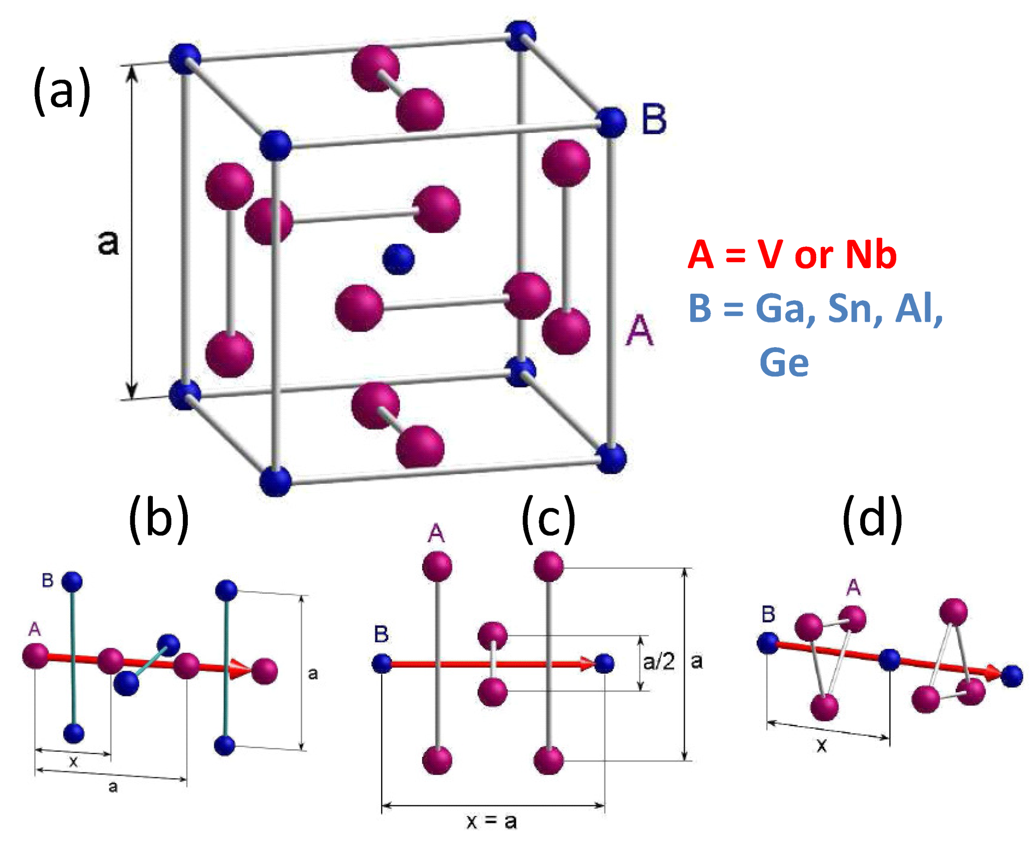
  • Direction (1) along the A-A atoms following the faces of the unit cell (b). The distance between the A atoms is x = a / 2 . In this direction, two B atoms will be passed, which have a distance of l B = a / 2 = x . The relation l B / x = 1, which is much larger than x / 2 , so an influence can be excluded.
  • Direction (2) along the B-B atoms following the faces of the unit cell (c). The distance between the B atoms is x = a . Two A atoms will be passed, which have a distance of l A 1 = a / 4 , so there will be an influence. Further, there are four more atoms at a distance of l A 2 = a / 2 . The relation l A 2 / x = 1/2, but these atoms are not located in the main direction, so that an influence of them can be excluded.
  • Direction (3) along the B-B atoms following the space diagonal in the unit cell (d). The distance between the B atoms is x = 3 / 4 · a . There are three A atoms being passed, which have a distance of l A = 3 a / 16 . The relation is l A / x = 3 / 8 , so that there is certainly an influence of these atoms, which must be taken into account.
The unit cell of the A15 structure is a complicated one, so we have to consider the relations of the directions to each other in the main c direction. Direction (1) appears in one spatial direction twice, but these belong to two elementary cells, so that it follows 2 · 1 / 2 = 1 . Direction (2) exists in one spatial direction four times along the unit cell edges and once along the space centered B atom of one unit cell to the next one. This direction belongs only to this unit cell, while in the former case, each direction belongs to four unit cells, so we have 4 · 1 / 4 + 1 = 2 . Direction (3) seems to appear at first glance only once in a spatial direction, but to obtain a clearer image, we must consider a sectional view of the unit cell, see Figure 7. Here, one can see that the edge of the unit cell is now a rectangle. As a consequence, Direction (3) exists four times along the edges of the unit cell and once in the center. Again, the edges belong to four unit cells each and the center only to one unit cell. Thus, we have a factor of two.
In total, we obtain now the relation:
1 × direction ( 1 ) + 2 × direction ( 2 ) + 2 × direction ( 3 ) ,
which was found to hold for all A15 compounds investigated here.
Table 4 summarizes some of the results obtained for the compounds V 3 Si, Nb 3 Ga, Nb 3 Sn, Nb 3 Al and Nb 3 Ge. For the experimental data, T c (exp), only data for bulk and wire samples were used. However, not in all cases were data for the transition width given in the literature, which would allow deducing the required T c , midpoint properly. Thus, some experimental data were not useful for a comparison. Data for the compounds V 3 Ga, V 3 Ge and V 3 Al were also obtained in [33] with T c , ( 0 ) values close to the reported experimental values. The hypothetical compound Nb 3 Nb (the prepared material requires a small addition of Ge to stabilize the phase [84]) cannot be calculated with the same electron configuration as for the other materials, as it is obvious that any T c obtained in Direction (1) with one electron only would give a T c of ∼10 K. An important piece of information comes from band structure calculations by Ho et al. [90], who explained the decrease of T c by softening the bonding on the Nb chains (which corresponds to Direction (1) here) and coupling of neighboring chains. If we assume two charge carriers of Nb for all directions, we obtain a T c of 6.35 K when summing up all three contributions in a simple fashion. This value comes close to the estimated T c of 6 K [84].
The case of Nb 3 Ge is again an interesting one, as the maximum experimentally observed T c value is obtained in thin films. The result for T c obtained here is 19.13 K, being close to that of bulk materials. If we apply the same idea as for Al that the substrate may enable the superconducting direction to be excluded from the calculation, we would have a contribution from Direction (2) as well, which would give 22.95 K as the maximum achievable T c in this system, which is again close to the experimentally observed values. This is again a hint to investigate the thickness dependence of T c in more detail.
In summary, for the various A15 compounds, the calculations using the Roeser–Huber equation give reasonable results for the superconducting transition temperatures.

4.8. MgB 2

Superconductivity in the MgB 2 system was found by Akimitsu et al. in 2001 [5]. The T c of MgB 2 of 39 K nearly doubled the previous record for the highest T c of an alloy held by Nb 3 Ge with 23.2 K [98,99]. The MgB 2 crystal lattice shows two different atomic bindings, the covalent ones, which are mostly typical for semiconductors, and also metallic binding, being typical for conductive materials. Interestingly, both constituents are not individual superconductors, and both Mg and B are light elements, which do not have d-electrons. Mg can be considered as ionized [100], as the two s-electrons are donated and are now part of the B conduction band [101]. In the B plane, there are the covalent bindings (2D σ ) between the B atoms. These covalent bindings are strong, whereas the coupling between B and Mg between the layers is formed by metallic 3D π bindings, which provide a weak coupling only [102]. Furthermore, the bindings within the Mg plane are much stronger than the Mg-B bindings [98]; thus, cleaving of the crystal can take place at this position [103]. The electronic structure of MgB 2 shows four bands crossing the Fermi level [104]. Two π bands, which result from the p z -orbitals of the B atoms, are weakly coupled with the phonon modes (3D character). The two σ bands result from the p x , y orbitals of the B atoms. These are weakly coupled to the phonon modes (2D character) [102,105,106]. MgB 2 is in the normal conducting state a hole conductor, and the Hall coefficient is positive [98]. There is one 3D electron-type binding and 3D hole conducting binding, where the latter one is mainly in c direction [102]. Calculations by Palecchi et al. [105] also showed that at least one π band shows electron conduction. A two band or even multiband superconductivity is well understood and corroborated by various experiments like point contact spectroscopy or tunneling experiments [106,107,108,109,110]. The consequence from this is that there are several pairing energies in the system [111]. Furthermore, there have been recently speculations that MgB 2 could belong to a new type of superconductor exhibiting similarities between Type-I and Type-II superconductivity, based on observations of the flux-line lattice [112].
The crystal structure of MgB 2 is hexagonal of the the type AlB 2 (space group C32, P6/mmm). The magnesium and boron atoms are arranged in sequent layers (see Figure 8a). The lattice parameters are a = 0.3047 nm and c = 0.3421 nm. The shortest distance between atoms is the B-B-spacing within the B-layer with d = 0.176 nm.
There are four distinct main directions in the crystal lattice, which are are represented in Figure 8b–e. A fifth direction along the space diagonal has unsymmetric passages and is therefore not relevant for our considerations.
  • Direction (1) along the Mg-Mg atoms within the Mg plane (b): The distance between the Mg atoms is x = a = 0.3047 nm. The charge carriers along this direction will pass 4 B atoms, 2 from the layer below and 2 from the layer above. Furthermore, two Mg atoms from the same layer are passed as well. The distances are l B = 0.192 nm (B) with l B / x = 0.630 and l M g = 0.264 nm with the relation l M g / x = 0.866. Thus, the distances to the neighboring atoms are too big to have an influence on the superconductivity.
  • Direction (2) along the Mg-Mg atoms within the Mg layer (c): The distance between the Mg atoms is x = 2 3 · a / 2 = 0.528 nm. The passed atoms are the same as in Direction (1), but the distances are different: l B = c / 2 = 0.171 ( l B / x = 0.324) and l M g = a / 2 = 0.152 nm with l M g / x = 0.288 nm. All distance ratios are smaller than 0.5, so all six atoms have an influence.
  • Direction (3) along the Mg-Mg atoms in the c direction (d): The distance between the Mg atoms is x = c = 0.3421 nm. In this direction, a hexagon of B atoms is passed. The corresponding distance is l B = 0.176 nm, and the relation l B / x = 0.514, which is close to 0.5.
  • Direction (4): along the B-B atoms in the c direction (e). The distance between the boron atoms is x = c = 0.3421 nm. In this direction, three Mg atoms arranged in a triangle are passed, which have the same short distance to the main direction. The distance between the Mg atoms and the charge carrier direction is l M g = 2 / 3 h = 0.176 nm, where h denotes the height of the triangle. The relation l M g / x = 0.514, so an influence on the charge carriers is proposed.
The calculation of T c in the MgB 2 system was shown to be quite complex due to the multimode character of the superconductivity. Thus, we give here only a short summary of the findings [33].
Superconductivity in MgB 2 may take place via three directions along Mg chains and one direction along B with N L = 2 and n 2 R 1 3 = 1. Two distinctly different possibilities exist for the calculation of T c , using (i) one electron for the directions employing Mg atoms and (ii) two electrons. The electronic configuration of Mg (Mg 2 + ) indicates Case (ii). Furthermore, the sum of all experimental facts thus favors the second possibility, which will be presented here.
In the (a,b) plane, we have in Direction (1) N atom = 0, so M L = 2 m p . In Direction (2), we have N atom = 6, so M L = 0.333 m p . Summing up the individual pairing energies (Equation (8)), one obtains Δ a b ( 0 ) = 3.307 meV, and finally, using Equation (6) T c ( 0 ) a b = 12.22 K. This value is clearly too small when compared to the experimental values. This result points to a problem concerning the effective mass employed in the calculations, as at least one band shows electron conductivity. Therefore, this should be further analyzed in future works.
In the c direction, one uses in Direction (3) N atom = 6, which yields M L = 0.333, and in Direction (4) N atom = 3 with M L = 0.666. Using Equations (6) and (8), one obtains Δ c ( 0 ) = 7.875 meV, and finally, T c ( 0 ) c = 38.79 K with n 2 R 3 = 1 and n 2 R 4 = 2.
The obtained value for T c ( 0 ) c = 38.79 K is again very close to the experimentally obtained data and places MgB 2 on the common line with the other superconducting materials investigated.

5. Discussion

To summarize, we presented here a number of calculations of the superconducting transition temperature, based on an approach of Roeser et al. [26]. The more complicated and complex crystal structures of the fcc metals and the superconducting two component superconductors NbN, A15 and MgB 2 required a refinement of the calculation procedure regarding the possible superconducting directions in the crystal lattices. For this purpose, several selection criteria were evaluated and new correction factors were introduced. The final equation, called the Roeser–Huber equation (Equation (6)), combined the calculation processes of the HTSc and the metallic superconductors.
Figure 9 presents the results of all calculations for the simple metallic alloys calculated here and in [33]. All data fall within a small error margin on a straight line, as was already shown in the first analysis on the bcc metals by Roeser et al. [31]. The obtained slope is 2.9813 × 10 18 m 2 K, and the y-axis intersect is 0.0052 × 10 18 m 2 K. The theoretical value would be m = h 2 / ( 2 π k B m p ) = 3.02586 × 10 18 m 2 K. The deviation is 0.10756 × 10 18 m 2 K (3.55%), which is less exact as compared to the results obtained on various HTSc materials [26,27,28]. This may point out that some more refinements may be required to describe all the various crystal structures properly. If we take the quotient of the slope of the HTSc data and that of the present data, we obtain:
5555.17 · 10 18 m 2 K 2.9183 · 10 18 m 2 K = 1903.56 .
The quotient of proton mass and electron mass is:
m p m e = 1836.15 ,
with a deviation of 3.67%. The relation being this close confirms the assumption that a charge carrier mass of the dimension of the proton mass is required to describe the metallic superconductors in the Roeser–Huber equation.
When now taking the charge carrier mass into the diagram, it becomes possible to combine all the results shown here with those of the calculations of T c for a large number of high T c superconductors. The final diagram is presented in Figure 10. All data fall on a common straight line with only a small error margin. From a least squares fit to the data, we obtain a slope m = 4.998 × 10 45 m 2 kg K and an axis intersect of 0.0047 × 10 45 m 2 kg K. The theoretical value, m = h 2 / 2 π k B ) , equals 5.06112 × 10 45 m 2 kg K. The obtained deviation is just 1.23%, which is remarkably small.
A central finding of the present calculations is that the charge carrier mass being approximately equal to the size of the proton mass is common for all metallic superconductors and thus clearly distinct from the HTSc compounds, where the electron mass is employed. This high charge carrier mass, m L , is a result from incorporating all correction factors here. Of course, the charge carriers in the metallic superconductors are electrons or holes forming the Cooper pairs. Thus, we could also write m L = m e · μ instead, and the correction factor μ would contain all the additional information. For the sake of having a unified expression for both HTSC and metallic superconductors, we adopted the first way of presentation. This directly distinguishes the metallic superconductors from the HTSc: in HTSc, the charge carrier wave interacts solely with a characteristic doping distance in the crystal lattice, whereas the charge carrier wave of the metallic superconductors interacts with a characteristic interatomic distance, and the effect of neighboring atoms must be taken into account. It will be interesting to see how this principle will develop in other superconductor systems like heavy fermion superconductors or organic superconductors. The present calculations on MgB 2 already demonstrated that in the c direction, the description of a metallic superconductor worked well, as in the c direction, we had a metallic interaction between the layers, whereas in the (a,b) direction, this principle was not valid due to the strong covalent bindings in the boron layer, where one might need to assume an HTSc behavior in order to find a crystal direction for an electron based charge carrier wave. The complete understanding of the properties of MgB 2 is thus another very interesting topic for future work.
Even though some of the assumptions made in the calculations (e.g., charge carrier mass, number of electrons involved, excluding of some charge carrier directions, etc.) still require a deeper theoretical foundation, the success of obtaining reasonable T c values for various distinctly different materials and crystal lattices by regarding only the details of the respective crystal structure is remarkable and justifies the assumptions made.
Having obtained all these results for the superconducting transition temperatures via the Roeser–Huber equation, one may ask three important questions:
(1)
Will it be possible to analyze also the change of T c when applying pressure to the material?
(2)
Is it possible to find an explanation to the T c dependence on the sample thickness of thin films?
(3)
Can we make predictions concerning new superconductor materials?
Question (1) was answered in a more recent study [113], and the answer is yes, the Roeser–Huber equation can reproduce the pressure dependence of T c , provided that proper crystallographic data are available. For Question (2), there are already some interesting hints (see, e.g., the calculation of T c of Al), but up to now, the analysis of thin films was excluded from the analysis in order to avoid substrate effects. This will be clearly one direction for further work. The most challenging Question (3) is another possible goal. The need to know only the details of the crystal structure and the electronic configuration enables a straightforward calculation of T c in various combinations. However, up to now, we have not attempted to make predictions of possible, new superconductors. One way to go may be the computer aided design of new superconducting materials [114,115,116], which would require the use of databases containing also the crystallographic information.

6. Outlook

As already mentioned, several assumptions made in the calculation process need further theoretical consideration and a proper foundation. Nevertheless, the calculation of the superconducting transition temperature of many metallic superconductors is possible using the Roeser–Huber equation, using several refinements to cover the properties of the complicated crystal structures found for metallic alloys like the A15 compounds or MgB 2 . Furthermore, for metallic alloys and systems with more constituents, one might consider another correction factor describing the chemical environment of a superconducting path including the atoms in the path, as well as the atoms passed, which is presently not the case. The need for such correction is already seen in the calculation of the NbTi alloy and may refine also the calculations of the A15 compounds. This will make the Roeser–Huber equation a useful tool for the computer aided design of new superconducting materials [114,115,116]. Even more superconducting systems have to be analyzed in detail, including the superconductivity in the (a,b) plane of MgB 2 . The consideration of thin films and the dependence of T c on the film thickness and the type of substrate will be the next challenge for the application of the Roeser–Huber equation.

7. Conclusions

To conclude, we showed a calculation method and procedure of the superconducting transition temperature, T c , of several metallic superconductors and simple alloys, based on detailed considerations of the respective crystal structures. For a large number of superconductors, we could show that the data followed a straight line with only small deviations. Thus, the principle of calculating the superconducting transition temperatures using the details of the crystallographic information and the electronic configuration of the constituting elements seemed to be at least empirically a reasonable approach, even though several assumptions still require theoretical foundation.

Author Contributions

Conceptualization, M.R.K.; formal analysis, S.R., A.K.-V. and M.R.K.; investigation, A.W., T.K., X.L.Z., A.K.-V., and M.R.K.; supervision, S.F. and M.M.; writing, original draft preparation, S.R., A.K.-V., and M.R.K.; writing, review and editing, all authors. All authors have read and agreed to the published version of the manuscript.

Acknowledgments

This work is dedicated to H.P. Roeser (Institute of Space Systems, Stuttgart), who started these calculations and supervised most of the master and PhD students working on this topic. The work at Saarbrücken was subsidized by Volkswagen, DFG and ANR-DFG, which is gratefully acknowledged.

Conflicts of Interest

The authors declare no conflict of interest.

References

  1. Gutton, M. Annales de Chimie et de Physique; V. Masson: Paris, France, 1816. [Google Scholar]
  2. Onnes, H.K. Part I.—Laboratory methods of liquefaction. On the lowest temperature yet obtained. Trans. Faraday Soc. 1922, 18, 145–174. [Google Scholar] [CrossRef] [Green Version]
  3. van Delft, D.; Kes, P.H. The discovery of superconductivity. Phys. Today 2010, 63, 38–43. [Google Scholar] [CrossRef] [Green Version]
  4. Matthias, B.T.; Geballe, T.H.; Geller, S.; Corenzwit, E. Superconductivity of Nb3Sn. Phys. Rev. 1954, 95, 1435. [Google Scholar] [CrossRef]
  5. Nagamatsu, J.; Nakagawa, N.; Muranaka, T.; Zenitani, Y.; Akimitsu, J. Superconductivity at 39 K in magnesium diboride. Nature 2001, 410, 63–64. [Google Scholar] [CrossRef] [PubMed]
  6. Bednorz, J.G.; Müller, K.A. Possible high Tc superconductivity in the Ba-La-Cu-O system. Z. Phys. B Condens. Matter 1986, 64, 189–193. [Google Scholar] [CrossRef]
  7. Chu, C.W.; Hor, P.H.; Meng, R.L.; Gao, L.; Huang, Z.J.; Wang, Y.Q. Evidence for superconductivity above 40 K in the La-Ba-Cu-O compound system. Phys. Rev. Lett. 1987, 58, 405–407. [Google Scholar] [CrossRef] [Green Version]
  8. Wu, M.K. Superconductivity at 93 K in a new mixed-phase Y-Ba-Cu-O compound system at ambient pressure. Phys. Rev. Lett. 1987, 58, 908–910. [Google Scholar] [CrossRef] [Green Version]
  9. Gao, L. Superconductivity up to 164 K in HgBa2Cam-1CumO2+2+δ (m= 1, 2, and 3) under quasihydrostatic pressures. Phys. Rev. B 1994, 50, 4260–4263. [Google Scholar] [CrossRef]
  10. Drozdov, A.P.; Eremets, M.I.; Troyan, I.A.; Ksenofontov, V.; Shylin, S.I. Conventional superconductivity at 203 kelvin at high pressures in the sulfur hydride system. Nature 2015, 525, 73–76. [Google Scholar] [CrossRef]
  11. Drozdov, A.P.; Kong, P.P.; Minkov, V.S.; Besedin, S.P.; Kuzovnikov, M.A.; Mozaffari, S.; Balicas, L.; Balakirev, F.F.; Graf, D.E.; Prakapenka, V.B.; et al. Superconductivity at 250 K in lanthanum hydride under high pressures. Nature 2019, 569, 528–533. [Google Scholar] [CrossRef] [Green Version]
  12. Somayazulu, M.; Ahart, M.; Mishra, A.K.; Geballe, Z.M.; Baldini, M.; Meng, Y.; Struzhkin, V.V.; Hemley, R.J. Evidence for Superconductivity above 260 K in Lanthanum Superhydride at Megabar Pressures. Phys. Rev. Lett. 2019, 122, 027001. [Google Scholar] [CrossRef] [Green Version]
  13. Savitskii, E.M.; Baron, V.V.; Efimov, Y.V.; Bychkova, M.I.; Myzenkova, L.F. Superconducting Materials, 1st ed.; Plenum Press: New York, NY, USA; London, UK, 1973. [Google Scholar]
  14. Poole, C.P. (Ed.) Handbook of Superconductivity, 1st ed.; Elsever: Amsterdam, The Netherlands, 1995. [Google Scholar]
  15. Matthias, B.T. Chapter V Superconductivity in the Periodic System. Prog. Low Temp. Phys. 1957, 2, 138–150. [Google Scholar] [CrossRef]
  16. Matthias, B.T.; Geballe, T.H.; Compton, V.B. Superconductivity. Rev. Mod. Phys. 1963, 35, 1. [Google Scholar] [CrossRef]
  17. Conder, K. A second life of the Matthias’ rules. Supercond. Sci. Technol. 2016, 29, 080502. [Google Scholar] [CrossRef]
  18. Kinjo, T.; Kajino, S.; Nishio, T.; Kawashima, K.; Yanagi, Y.; Hase, I.; Yanagisawa, T.; Ishida, S.; Kito, H.; Takeshita, N.; et al. Superconductivity in LaBi3 with AuCu3-type structure. Supercond. Sci. Technol. 2016, 29, 03LT02. [Google Scholar] [CrossRef]
  19. McMillan, W.L. Transition Temperature of Strong-Coupled Superconductors. Phys. Rev. 1968, 167, 331–334. [Google Scholar] [CrossRef]
  20. Seiden, P.E. Calculation of the Superconducting Transition Temperature. Phys. Rev. 1968, 168, 403–408. [Google Scholar] [CrossRef]
  21. Allen, P.B.; Cohen, M.L. Pseudopotential Calculation of the Mass Enhancement and Superconducting Transition Temperature of Simple Metals. Phys. Rev. 1969, 187, 525–538. [Google Scholar] [CrossRef]
  22. Kessel, W. On a general formula for the transition temperature of superconductors. Z. Naturforsch. 1974, 29a, 445–451. [Google Scholar] [CrossRef] [Green Version]
  23. Haufe, U.; Kerker, G.; Bennemann, K.H. Calculation of the superconducting transition temperature Tc for metals with phonon-anomalies. Solid State Commun. 1975, 17, 321–325. [Google Scholar] [CrossRef]
  24. Nowotny, H.; Hittmair, O. Calculation of the transition temperature Tc of superconductors. Phys. Stat. Solidi (B) 1979, 91, 647–656. [Google Scholar] [CrossRef]
  25. Arita, R.; Koretsune, T.; Sakai, S.; Akashi, R.; Nomura, Y.; Sano, W. Nonempirical Calculation of Superconducting Transition Temperatures in Light-Element Superconductors. Adv. Mater. 2017, 29, 1602421. [Google Scholar] [CrossRef] [PubMed]
  26. Roeser, H.P.; Haslam, D.T.; Hetflleisch, F.; Lopez, J.S.; von Schoenermark, M.F.; Stepper, M.; Huber, F.M.; Nikoghosyan, A.S. Electron transport in nanostructures: A key to high temperature superconductivity? Acta Astronaut. 2010, 67, 546–552. [Google Scholar] [CrossRef]
  27. Roeser, H.P.; Hetfleisch, F.; Huber, F.M.; Stepper, M.; von Schoenermark, M.F.; Moritz, A.; Nikoghosyan, A.S. A link between critical transition temperature and the structure of superconducting YBa2Cu3O7-δ. Acta Astronautica 2008, 62, 733–736. [Google Scholar] [CrossRef]
  28. Roeser, H.P.; Haslam, D.T.; Lopez, J.S.; Stepper, M.; von Schoenermark, M.F.; Huber, F.M.; Nikoghosyan, A.S. Electronic energy levels in high temperature superconductors. J. Supercond. Novel Mag. 2011, 24, 1443–1451. [Google Scholar] [CrossRef] [Green Version]
  29. Huber, F.; Roeser, H.P.; von Schoenermark, M.F. A correlation between Tc of Fe based HT Superconductors and the crystal superlattice constants of the doping element positions. J. Phys. Soc. Jpn. 2008, 77 (Suppl. C), 142–144. [Google Scholar] [CrossRef] [Green Version]
  30. Rohlf, J.W. Modern Physics from α to Z0; Wiley: New York, NY, USA, 1994. [Google Scholar]
  31. Roeser, H.P.; Haslam, D.T.; Lopez, J.S.; Stepper, M.; von Schoenermark, M.F.; Huber, F.M.; Nikoghosyan, A.S. Correlation between transition temperature and crystal structure of niobium, vanadium, tantalum and mercury superconductors. Acta Astronaut. 2010, 67, 1333–1336. [Google Scholar] [CrossRef]
  32. Moritz, A. Calculation of the Transition Temperature of One-Component-Superconductors. Master’s Thesis, Institute of Space Systems, University of Stuttgart, Stuttgart, Germany, 2009. (In German). [Google Scholar]
  33. Stepper, M. Calculation of the Transition Temperature of Two-Component-Superconductors. Master’s Thesis, Institute of Space Systems, University of Stuttgart, Stuttgart, Germany, (In German). 2008. [Google Scholar]
  34. ICDD. ICDD PDF Data Base; ICDD: Newtown Square, PA, USA, 2019. [Google Scholar]
  35. Materials Project Database V2019.05. Available online: https://materialsproject.org/ (accessed on 12 December 2019).
  36. Wördenweber, R. Mechanism of vortex motion in high temperature superconductors. Rep. Prog. Phys. 1999, 62, 187–236. [Google Scholar] [CrossRef]
  37. Koblischka, M.R. Magnetic Properties of High-Temperature Superconductors; Alpha Science International Ltd.: Oxford, UK, 2009; ISBN 978-1-84265-149-0. [Google Scholar]
  38. Pradhan, A.K.; Muralidhar, M.; Koblischka, M.R.; Murakami, M.; Nakao, K.; Koshizuka, N. Flux pinning in melt-processed ternary (Nd–Eu–Gd)Ba2Cu3Oy superconductors with Gd2BaCuO5 addition. J. Appl. Phys. 1999, 86, 5705–5711. [Google Scholar] [CrossRef]
  39. Chen, D.X.; Goldfarb, R.B. Kim model for magnetization of type-II superconductors. J. Appl. Phys. 1989, 66, 2489–2500. [Google Scholar] [CrossRef]
  40. Skumryev, V.; Koblischka, M.R.; Kronmüller, H. Sample size dependence of the AC-susceptibility of sintered YBa2Cu3O7-δ superconductors. Phys. C 1991, 184, 332–340. [Google Scholar] [CrossRef]
  41. Karwoth, T.; Furutani, K.; Koblischka, M.R.; Zeng, X.L.; Wiederhold, A.; Muralidhar, M.; Murakami, M.; Hartmann, U. Electrotransport and magnetic measurements on bulk FeSe superconductors. J. Phys. Conf. Ser. 2018, 1054, 012018. [Google Scholar] [CrossRef]
  42. Karwoth, T. Electronic Transport Measurements on Electrospun High-Tc Fibers. Master’s Thesis, Saarland University, Saarbrücken, Germany, 2016. [Google Scholar]
  43. Prozorov, R.; Shantsev, D.V.; Mints, R.G. Collapse of the critical state in superconducting niobium. Phys. Rev. B 2006, 74, 220511. [Google Scholar] [CrossRef] [Green Version]
  44. Pust, L.; Wenger, L.E.; Koblischka, M.R. Detailed investigation of the superconducting transition of niobium disks exhibiting the paramagnetic Meissner effect. Phys. Rev. B 1998, 58, 14191–14194. [Google Scholar] [CrossRef] [Green Version]
  45. Pust, L.; Wenger, L.E.; Koblischka, M.R. Details of the Superconducting Phase Transition in Nb showing the Paramagnetic Meissner Effect. Phys. Stat. Solidi (B) 1999, 212, R13–R14. [Google Scholar] [CrossRef]
  46. Wenger, L.E.; Pust, L.; Koblischka, M.R. Investigation of the paramgnetic Meissner effect on Nb disks. Phys. B 2000, 284–288, 797–798. [Google Scholar] [CrossRef]
  47. Hauser, J.J.; Theuerer, H.C. Superconducting Tantalum films. Rev. Mod. Phys. 1964, 36, 80–83. [Google Scholar] [CrossRef] [Green Version]
  48. Joshi, L.M.; Verma, A.; Gupta, A.; Rout, P.K.; Husale, S.; Budhani, R.C. Superconduting properties of NbN film, bridge and meanders. AIP Adv. 2018, 8, 055305. [Google Scholar] [CrossRef]
  49. Grawatsch, K. Grundlegende Untersuchungen über die Einsatzmöglichkeiten Supraleitender Schalter in der Kryogenen Energietechnik. Ph.D. Thesis, Zentralbibliothek d. Kernforschungsanlage, Jülich, Germany, 1974. [Google Scholar]
  50. Wiederhold, A.; Koblischka, M.R.; Inoue, K.; Muralidhar, M.; Murakami, M.; Hartmann, U. Electric transport measurements on bulk, polycrystalline MgB2 samples prepared at various reaction temperatures. J. Phys. Conf. Ser. 2016, 695, 012004. [Google Scholar] [CrossRef] [Green Version]
  51. Koblischka-Veneva, A.; Koblischka, M.R.; Schmauch, J.; Inoue, K.; Muralidhar, M.; Berger, K.; Noudem, J. EBSD analysis of MgB2 bulk superconductors. Supercond. Sci. Technol. 2016, 29, 044007. [Google Scholar] [CrossRef] [Green Version]
  52. Yamamoto, A.; Shimoyama, J.; Kishio, K.; Matsushita, T. Limiting factors of normal-state conductivity in superconducting MgB2: An application of mean-field theory for a site percolation problem. Supercond. Sci. Technol. 2007, 20, 658–666. [Google Scholar] [CrossRef]
  53. Ivry, Y.; Kim, C.-S.; Dane, A.E.; De Fazio, D.; McCaughan, A.N.; Sunter, K.A.; Zhao, Q.; Berggren, K.K. Universal scaling of the critical temperature for thin films near the superconducting-to-insulating transition. Phys. Rev. B 2014, 90, 214515. [Google Scholar] [CrossRef] [Green Version]
  54. Aschermann, G.; Friedrich, E.; Justi, E.; Kramer, J. Superconductive connections with extremely high cracking temperatures (NbH and NbN). Phys. Z. 1941, 42, 349–360. [Google Scholar]
  55. Guard, R.W.; Savage, J.W.; Swarthout, D.G. Constitution of a portion of the niobium (columbium)-nitrogen system. Trans. Met. Soc. AIME 1967, 239, 643–649. [Google Scholar]
  56. Brauer, G.; Kirner, H. Drucksynthese von Niobnitriden und von δ-NbN. Z. Anorg. Allg. Chem. 1964, 328, 34–43. [Google Scholar] [CrossRef]
  57. Geibel, C.; Rietschel, H.; Junod, A.; Pelizzone, M.; Müller, J. Electronic properties, phono densities of states and superconductivity in Nb1-xNx. J. Phys. F Met. Phys. 1985, 15, 405–416. [Google Scholar] [CrossRef]
  58. Roedhammer, P.; Gmelin, E.; Weber, W.; Remeika, J.P. Observation of phonon anomalies in NbxN1-x alloys. Phys. Rev. B 1977, 15, 711–717. [Google Scholar] [CrossRef]
  59. Meyer, O.; Friedland, E.; Scheerer, B. Superconductivity of niobium nitride single-crystals after implantation of carbon and nitrogen. Solid State Commun. 1981, 39, 1217–1221. [Google Scholar] [CrossRef]
  60. Bauer, H.; Saur, E.J.; Schweitzer, D.G. Effect of thermal-neutron irradiations on superconductivity of B-1 compounds doped with B-10 and U-235. J. Low Temp. Phys. 1975, 19, 189–200. [Google Scholar] [CrossRef]
  61. Pessall, N.; Gold, R.E.; Johansen, H.A. A study of superconductivity in interstitial compounds. J. Hys. Chem. Solids 1968, 29, 19–38. [Google Scholar] [CrossRef]
  62. Geballe, T.H.; Matthias, B.T.; Remeika, J.P.; Clogston, A.M.; Compton, V.B.; Maita, J.P.; Williams, H.J. High temperature SP-band superconductors. Phys. Phys. Fiz. 1966, 2, 293–310. [Google Scholar] [CrossRef] [Green Version]
  63. Horn, G.; Saur, E. Preparation and superconductive properties of niobium nitride and niobium nitride with admixtures of titanium, zirconium and tantalum. Z. Phys. 1968, 210, 70–79. [Google Scholar] [CrossRef]
  64. Rögener, H. Zur Supraleitung des Niobnitrids. Z. Phys. 1952, 132, 446–467. [Google Scholar] [CrossRef]
  65. Hechler, K.; Horn, G.; Otto, G.; Saur, E. Measurements of critical data for some type II superconductors and comparison with theory. J. Low Temp. Phys. 1969, 1, 29–43. [Google Scholar] [CrossRef]
  66. Glowacki, B.A. Development of Nb based conductors. In Frontiers of Superconducting Materials; Narlikar, A.V., Ed.; Springer: Berlin/Heidelberg, Germany, 2005; pp. 697–738. [Google Scholar]
  67. Seeber, B. (Ed.) Handbook of Applied Superconductivity; IOP Publishing: Bristol, UK, 1999. [Google Scholar]
  68. Cardwell, D.A.; Ginley, D.S. (Eds.) Handbook of Superconducting Materials; CRC Press: Boca Raton, FL, USA, 2002. [Google Scholar]
  69. Hillmann, H. Interaction of metallurgical treatment and flux pinning of NbTi superconductors. Supercond. Sci. Technol. 1999, 12, 348–355. [Google Scholar] [CrossRef]
  70. Hutchinson, T.S.; Ocampo, G.; Carpenter, G.J.C. Crystal structure and morphology in commercial NbTi (46.5 wt.-% Ti) superconducing fibers. Scr. Metall. 1985, 19, 635–638. [Google Scholar] [CrossRef]
  71. Steele, M.C.; Hein, R.A. Superconductivity of Titanium. Phys. Rev. 1953, 92, 243–247. [Google Scholar] [CrossRef]
  72. Gajda, D. Analysis Method of High-Field Pinning Centers in NbTi Wires and MgB2 Wires. J. Low Temp. Phys. 2019, 194, 166–182. [Google Scholar] [CrossRef] [Green Version]
  73. Shimizu, J.; Tonooka, K.; Yoshida, Y.; Furuse, M.; Takashima, H. Growth and superconductivity of niobium titanium alloy thin films on strontium titanate (001) single crystal substrates for superconducting joints. Sci. Rep. 2018, 8, 15135. [Google Scholar] [CrossRef] [Green Version]
  74. Lee, P.J. Abridged Metallurgy of Ductile Alloy Superconductors. Wiley Encyclopedia of Electrical and Electronics Engineering. 1999, Volume 24. Available online: http://fs.magnet.fsu.edu/~lee/asc/pdf_papers/589.pdf (accessed on 12 December 2019).
  75. Cooley, L.; Lee, P.J.; Larbalestier, D.C. Processing of Low Tc Conductors. In Handbook of Superconducting Materials; Seeber, B., Ed.; Institute of Physics Publishing: Bristol, UK, 2003; pp. 603–639. [Google Scholar]
  76. Meingast, C.; Larbalestier, D.C. Quantitative description of a very high critical current-density Nb-Ti superconductor during its final optimization strain. 2. Flux pinning mechanism. J. Appl. Phys. 1989, 66, 5971–5983. [Google Scholar] [CrossRef]
  77. Hardy, G.F.; Hulm, J.K. The Superconductivity of Some Transition Metal Compounds. Phys. Rev. 1954, 93, 1004–1016. [Google Scholar] [CrossRef]
  78. Hulm, J.K.; Matthias, B.T. High-field, high-current superconductors. Science 1980, 208, 881–887. [Google Scholar] [CrossRef] [PubMed]
  79. Stewart, G.A. Superconductivity in the A15 structure. Phys. C 2015, 514, 28–35. [Google Scholar] [CrossRef] [Green Version]
  80. Matthias, B.T.; Geballe, T.H.; Longinotti, L.D.; Corenzwit, E.; Hull, G.W.; Willens, R.H.; Maita, J.P. Superconductivity at 20 degrees Kelvin. Science 1967, 156, 645–646. [Google Scholar] [CrossRef] [PubMed]
  81. Webb, G.W.; Vieland, L.J.; Miller, R.E.; Wicklund, A. Superconductivity above 20 degrees K in stoichiometric Nb3Ga. Solid State Commun. 1971, 9, 1769–1773. [Google Scholar] [CrossRef]
  82. Gavaler, J.R.; Janocko, M.A.; Jones, C.K. Preparation and properties of high Tc Nb-Ge thin films. J. Appl. Phys. 1974, 45, 3009–3012. [Google Scholar] [CrossRef]
  83. Testardi, L.R.; Wernick, J.H.; Royer, W.A. Superconductivity with onset above 23 K in Nb-Ge sputtered films. Solid State Commun. 1974, 15, 1–4. [Google Scholar] [CrossRef]
  84. Stewart, G.A.; Newkirk, L.A.; Valencia, F.A. Impurity stabilized A15 Nb3Nb—A new superconductor. Phys. Rev. B 1980, 21, 5055–5064. [Google Scholar] [CrossRef]
  85. Ballarino, A.; Hopkins, S.C.; Simon, C.; Bordini, B.; Richter, D.; Tommasini, D.; Bottura, L.; Benedikt, M.; Sugano, M.; Ogitsu, T.; et al. The CERN FCC Conductor Development Program: A Worldwide Effort for the Future Generation of High-Field Magnets. IEEE Trans. Appl. Supercond. 2019, 29, 6000709. [Google Scholar] [CrossRef] [Green Version]
  86. Kawashima, S.; Kawarada, T.; Kato, H.; Murakami, Y.; Sugano, M.; Oguro, H.; Awaji, S. Development of a High Current Density Distributed Tin Method Nb3Sn Wire. IEEE Trans. Appl. Supercond. 2020, 30, 6000105. [Google Scholar] [CrossRef]
  87. Hishinuma, Y.; Taniguchi, H.; Kikuchi, A. Development of the internal matrix reinforcement bronze processed Nb3Sn multicore wires using Cu-Sn-In ternary alloy matrix for fusion magnet application. Fusion Eng. Des. 2019, 148, 111269. [Google Scholar] [CrossRef]
  88. Testardi, L.R. Structural instability and superconductivity in A-15 compounds. Rev. Mod. Phys. 1975, 47, 637–648. [Google Scholar] [CrossRef]
  89. Sayeed, M.N.; Pudasaini, U.; Reece, C.E.; Eremeev, G.; Elsayed-Ali, H.E. Structural and superconducting properties of Nb3Sn films grown by multilayer sequential magnetron sputtering. J. Alloys Compd. 2019, 800, 272–278. [Google Scholar] [CrossRef]
  90. Ho, K.M.; Pickett, W.E.; Cohen, M.L. Electronic properties of Nb3Ge and Nb3Al from self-consistent pseudopotentials. II. Bonding, electronic charge distributions, and structural transformation. Phys. Rev. B 1979, 19, 1751–1761. [Google Scholar] [CrossRef]
  91. Lowrey, W.H. Hall effect in V3Si. J. Less-Common Met. 1979, 58, 99–100. [Google Scholar] [CrossRef]
  92. Huang, C.C.; Goldman, A.M.; Toth, L.E. Specific heat of a transforming V3Si crystal. Solid State Commun. 1980, 33, 581–584. [Google Scholar] [CrossRef]
  93. Foner, S.; McNiff, E.J., Jr.; Webb, G.W.; Vieland, L.J.; Miller, R.E.; Wicklund, A. Upper critical fields of NbxGa1-x—binary high temperature superconductor. Phys. Lett. 1972, 38A, 323–324. [Google Scholar] [CrossRef]
  94. Guritanu, V.; Goldacker, W.; Bouquet, F.; Wang, Y.; Lortz, R.; Goll, G.; Junod, A. Specific heat of Nb3Sn: The case for a second energy gap. Phys. Rev. B 2004, 70, 184526. [Google Scholar] [CrossRef] [Green Version]
  95. Junod, A.; Jorda, J.L.; Pelizzone, M.; Muller, J. Specific heat and magnetic susceptibility of nearly stoichiometric and homogeneous Nb3Al. Phys. Rev. B 1984, 29, 1189–1198. [Google Scholar] [CrossRef]
  96. Webb, G.W.; Matthias, B.T. Influence of composition on superconducting transition temperature of alloys with A-15 structure. Solid State Commun. 1977, 21, 193–194. [Google Scholar] [CrossRef]
  97. Vereshchagin, L.F.; Savitskii, E.M.; Evdokimova, V.V.; Novokshenov, V.I.; Petrenko, V.G. Effect of high pressures and temperatures on superconducting properties of compound Nb3Ge with A-15 structure. JETP Lett. 1976, 24, 193–194. [Google Scholar]
  98. Buzea, C.; Yamashita, T. Review of the superconducting properties of MgB2. Supercond. Sci. Technol. 2001, 14, R115–R146. [Google Scholar] [CrossRef] [Green Version]
  99. Muranaka, T.; Akimitsu, J. Superconductivity in MgB2. Z. Kristallogr. 2011, 226, 385–394. [Google Scholar] [CrossRef] [Green Version]
  100. Kurmaev, E.Z.; Lyakhovskaya, I.I.; Kortus, J.; Moewes, A.; Miyata, N.; Demeter, M.; Neumann, M.; Yanagihara, M.; Watanabe, M.; Muranaka, T.; et al. Electronic structure of MgB2: X-ray emission and absorption studies. Phys. Rev. B 2002, 65, 134509. [Google Scholar] [CrossRef] [Green Version]
  101. Kortus, J.; Mazin, I.I.; Belashchenko, K.D.; Antropov, V.P.; Boyer, L.L. Superconductivity of Metallic Boron in MgB2. Phys. Rev. Lett. 2001, 86, 4656–4659. [Google Scholar] [CrossRef] [Green Version]
  102. Belashchenko, K.D.; van Schilfgaarde, M.; Antropov, V.P. Coexistence of covalent and metallic bonding in the boron intercalation superconductor MgB2. Phys. Rev. B 2001, 64, 092503. [Google Scholar] [CrossRef] [Green Version]
  103. Das, S.K.; Bedar, A.; Kannan, A.; Jasuja, K. Aqueous dispersions of few-layer-thick chemically modified magnesium diboride nanosheets by ultrasonication assisted exfoliation. Sci. Rep. 2015, 5, 10522. [Google Scholar] [CrossRef] [Green Version]
  104. Souma, S.; Machida, Y.; Sato, T.; Takahashi, T.; Matsui, H.; Wang, S.-C.; Ding, H.; Kaminski, A.; Campuzano, J.C.; Sasaki, S.; et al. The origin of multiple superconducting gaps in MgB2. Nature 2003, 423, 65–67. [Google Scholar] [CrossRef]
  105. Pallecchi, I.; Ferrando, V.; Galleani D’Agliano, E.; Marré, D.; Monni, M.; Putti, M.; Tarantini, C.; Gatti, F.; Aebersold, H.U.; Lehmann, E.; et al. Magnetoresistivity as a probe of disorder in the π and σ bands of MgB2. Phys. Rev. B 2005, 72, 184512, Erratum in 2006, 73, 029901. [Google Scholar] [CrossRef] [Green Version]
  106. Gonnelli, R.S.; Daghero, D.; Ummarino, G.A.; Stepanov, V.A.; Jun, J.; Kazakov, S.M.; Karpinski, J. Direct Evidence for Two-Band Superconductivity in MgB2 Single Crystals from Directional Point-Contact Spectroscopy in Magnetic Fields. Phys. Rev. Lett. 2002, 89, 247004. [Google Scholar] [CrossRef] [Green Version]
  107. Dolgov, O.V.; Gonnelli, R.S.; Ummarino, G.A.; Golubov, A.A.; Shulga, S.V.; Kortus, J.J. Extraction of the electron-phonon interaction from tunneling data in the multigap superconductor MgB2. Phys. Rev. B 2003, 68, 132503. [Google Scholar] [CrossRef] [Green Version]
  108. Gonnelli, R.S.; Daghero, D.; Ummarino, G.A.; Stepanov, V.A.; Jun, J.; Kazakov, S.M.; Karpinski, J. Independent determination of the two gaps by directional point-contact spectroscopy in MgB2 single crystals. Supercond. Sci. Technol. 2003, 16, 171–175. [Google Scholar] [CrossRef] [Green Version]
  109. Daghero, D.; Gonnelli, R.S.; Ummarino, G.A.; Calzolari, A.; Dellarocca, V.; Stepanov, V.A.; Kazakov, S.M.; Jun, J.; Karpinski, J. Effect of the magnetic field on the gaps of MgB2: A directional point-contact study. J. Phys. Chem. Solids 2006, 67, 424–427. [Google Scholar] [CrossRef]
  110. Silva-Guillen, J.A.; Noat, Y.; Cren, T.; Sacks, W.; Canadell, E.; Ordejon, P. Tunneling and electronic structure of the two-gap superconductor MgB2. Phys. Rev. B 2015, 92, 064514. [Google Scholar] [CrossRef] [Green Version]
  111. Choi, H.J.; Roundy, D.; Sun, H.; Cohen, M.L.; Louie, S.G. The Origin of the Anomalous Superconducting Properties of MgB2. Nature 2002, 418, 758–760. [Google Scholar] [CrossRef]
  112. Moshchalkov, V.; Menghini, M.; Nishio, T.; Chen, Q.H.; Silhanek, A.V.; Dao, V.H.; Chibotaru, L.F.; Zhigadlo, N.D.; Karpinski, J. Type-1.5 Superconductivity. Phys. Rev. Lett. 2009, 102, 117001. [Google Scholar] [CrossRef] [Green Version]
  113. Roth, S. Theoretical Investigation of One-Component-Superconductors and their Relationship between Transition Temperature and Ionization Energy, Crystal Parameters and Further Parameters. Ph.D. Thesis, Institute of Space Systems, University of Stuttgart, Stuttgart, Germany, 2018. (In German). [Google Scholar]
  114. Gou, H.; Dubrovinskaia, N.; Bykova, E.; Tsirlin, A.A.; Kasinathan, D.; Schnelle, W.; Richter, A.; Merlini, M.; Hanfland, M.; Abakumov, A.M.; et al. Discovery of a Superhard Iron Tetraboride Superconductor. Phys. Rev. Lett. 2013, 111, 157002. [Google Scholar] [CrossRef] [Green Version]
  115. Stanev, V.; Oses, C.; Kusne, A.G.; Rodriguez, E.; Paglione, J.; Curtarolo, S.; Takeuchi, I. Machine learning modeling of superconducting critical temperature. NPJ Comput. Mater. 2018, 4, 29. [Google Scholar] [CrossRef]
  116. Matsumoto, K.; Horide, T. An acceleration search method of higher Tc superconductors by a machine learning algorithm. Appl. Phys. Express 2019, 12, 073003. [Google Scholar] [CrossRef]
Figure 1. A sketch of a crystal direction where the Cooper pairs can move along and the atoms passed. As an example, a NaCl-type crystal structure is shown with the atoms on the A-site depicted in dark green and the atoms on the B-site in light green. Assuming that the direction of the charge carrier wave λ cc (superconducting direction) is along the atoms on the A-site, then several atoms on the B-site must be passed in a distance l B as indicated. The situation shown corresponds to the direction (1) of the NbN superconductor (see Section 4.5). The characteristic distance x = λ c c / 2 is indicated as well.
Metals 10 00158 g001
Figure 2. Experimental determination of the superconducting transition temperature, T c , from resistance data as shown in (a) for a polycrystalline, bulk MgB 2 sample. In (a), the superconducting transition is presented. The plot (b) gives the derivative of the resistance data, with the peak position yielding T c , midpoint . The transition width, δ T c , is obtained as the peak width. (c) presents the most common approaches. T c , onset is obtained from the first deviation of the fitted linear behavior to the data above T c . The arrows indicate the problems arising when determining the first onset temperature. Another approach is the crossing point of two linear fits to the data above T c and to the transition part, also shown in (c). Finally, (d) gives a schematic comparison, which is really measured in the magnetic DC and AC methods and the resistance data.
Metals 10 00158 g002
Figure 3. Resistivity measured on several metallic superconductors. (a) Pb wire, (b) Nb wire, (c) Ta wire, (d) NbN thin film, (e) NbTi wire and (f) MgB 2 (bulk, polycrystalline material). The insets give details of the superconducting transitions and the residual resistivity, ρ 0 .
Metals 10 00158 g003
Figure 4. Relation of 2 x 2 vs. 1 / T c for the superconducting elements with fcc structure. For T c , experimental data are used. The horizontal error bars are determined by the variation of T c from sample to sample or from the uncertainty when using the literature data. This graph represents the situation when [31] was written. The data of Pb and Al are calculated via the PiB principle (shortest interatomic distance). The blue line gives the fit obtained by Roeser et al. [31] for the elements Nb, Hg, V and Ta. Fit (1) and Fit (2) are linear fits to the data with different weight with respect to the data of Pb and Al, and the two arrows indicate the direction of the changes required.
Metals 10 00158 g004
Figure 5. (ad) Crystallographic directions (1) to (4) for the charge carriers in the fcc crystal structure, allowing identifying the atoms passed (see main text).
Metals 10 00158 g005
Figure 6. A15 crystal structure (a) and the main directions for the charge carriers with neighboring atoms (bd).
Metals 10 00158 g006
Figure 7. View of the A15 crystal structure in Direction (3), the diagonal in space, which is pointing out of the plane. In the center, a 3D cube is shown to provide a connection to the three dimensionality. Direction (3) is oriented along the B-B atoms, which are marked by numbers accounting for the sharing of the atoms between neighboring unit cells: 1/4 implies that this atom belongs to four neighboring unit cells, and this direction exists four times in the crystal. The 1 indicates that this atom belongs only to one unit cell, and this direction exists only once.
Metals 10 00158 g007
Figure 8. (a) Crystal structure of MgB 2 and the four directions for the charge carriers (be).
Metals 10 00158 g008
Figure 9. The relation between the crystal structure and T c of the metallic simple alloys calculated here and in [33].
Metals 10 00158 g009
Figure 10. Compiled data of all metallic superconductors, the metallic alloys and most of the HTSc samples [26,27,28,31,32,33]. All data fall on a common straight line with only a small error margin. The iron based superconductors (IBS) superconductor SmO 1 δ F δ FeAs with the highest T c of the 1111-family is abbreviated as SOFFA, and the data of the various other 1111-family members investigated in [29] are not labeled.
Metals 10 00158 g010
Table 1. The distance x, ( 2 x ) 2 , the charge carrier mass M L and the calculated energies for all 4 directions in the fcc structure.
Directionx (10 10 m)(2x) 2 (10 19 m 2 ) M L ( 1 / m p ) Δ ( 0 ) [10 23 J]
13.54.946.69
24.959.8113.4
36.0614.724.46
48.5829.42/36.69
Table 2. The distance x, ( 2 x ) 2 , the charge carrier mass M L and the calculated energies for all 4 directions in the fcc structure.
Directionx (10 10 m)(2x) 2 (10 19 m 2 ) M L ( 1 / m p ) Δ ( 0 ) (10 23 J)
12.863.28133.08
24.056.5613/46.16
34.969.8413/22.05
47.0119.713/63.08
Table 3. The crystal parameter a 0 , the distance x, N L , N atoms , M L , the calculated energies and the calculated T c ( 0 ) .
a 0 (nm)x (nm) N L N atoms M L ( 1 / m p ) Δ ( 0 ) (meV) T c ( 0 ) (K)
0.4360.308120.54.3115.92
0.43930.311120.54.2415.68
Table 4. Data obtained for the A15 compounds. Listed are the lattice parameter a, the experimentally obtained T c (exp), the distance x for Directions (1)–(3), the calculated Δ ( 0 ) calc and T c , ( 0 ) calc for each direction and the final Δ ( 0 ) and T c , ( 0 ) . The sources of the experimental data are given as well. Note that we focus here on bulk-type materials only.
Compound a 0 (nm) T c (exp) (K)x (nm) Δ ( 0 ) calc (meV) T c , ( 0 ) calc (K) Δ ( 0 ) (meV) T c , ( 0 ) (K)
V 3 Si0.47216.80.2360 (1)1.8396.794.59716.98
[91]0.4720 (2)0.4601.70
[92]0.4088 (3)0.9193.39
Nb 3 Ga0.516520.20.2584 (1)3.07111.345.37519.86
[93]0.5165 (2)0.3841.42
0.4473 (3)0.7682.84
Nb 3 Sn0.52918.050.2645 (1)2.92710.814.87918.02
[94]0.5290 (2)0.4881.80
0.4581 (3)0.9763.60
Nb 3 Al0.51818.40.2590 (1)3.05311.285.08918.8
[95]0.5180 (2)0.5091.88
[96]0.4486 (3)1.0183.76
Nb 3 Ge0.513519.70.2568 (1)3.10711.485.17919.13
[97]0.5135 (2)0.5181.91
0.4447 (3)1.0363.83

