1. Introduction
Additive manufacturing is an effective method for the fabrication of prototypes and components for industrial use, enabling faster and more economical production of (increasingly complex) parts [
1]. The additive approach builds a component by bonding (small) units of material, such as powder or metal sheets, together into a larger piece. By controlling where these small material units are bonded, a (near-)net shape geometry may be obtained. There are many different additive manufacturing technologies, with the most common of these using high energy beams, such as lasers, to induce material bonding [
1]. As a result, many metal additive manufacturing technologies are fusion-based and rely on melting and subsequent solidification of the feedstock material in order to achieve metallurgical bonding.
Several limitations arise from the use of fusion-based approaches for additive manufacturing. For example, the resulting components nominally have anisotropic properties (due to the solidified, columnar microstructure), alloys can undergo constitutional undercooling, and the processing must be carefully controlled and monitored to prevent casting-type defects from occurring [
1]. In contrast, solid-state technologies, such as binder-jetting and ultrasonic methods, overcome these fusion limitations but have their own drawbacks [
2,
3]. These limitations include difficulties reaching full density (for binder-jet) and, for ultrasonic technologies, difficulty with residual stresses/strains in the build as well as limited ability to resolve fine component features.
Conversely, additive friction stir-deposition (AFS-D) is an emerging, solid-state material deposition process derived from the hollow rotation tool friction stir cladding technique developed and introduced by Van der Stelt et al. [
4,
5] and Liu et al. [
6]. AFS-D semi-continuously injects feedstock rods into the “deposition track” rather than using a non-consumable pin for processing as nominally done in friction stir welding (see
Figure 1a,b) [
7,
8,
9,
10,
11,
12]. By rastering the tool relative to the substrate, an approximate geometry may be obtained in a layer-by-layer fashion as each deposited layer metallurgical bonds to the deposited layer underneath it [
13]. As such, AFS-D is capable of high-throughput processing (up to 1000 cm
3/h) of a wide variety of metallic systems (including non-fusion-weldable alloys) to fabricate, repair, and join components. As a result, AFS-D can overcome some of the previously mentioned drawbacks of solid-state processing, such as the production of full density deposits [
12].
AFS-D deposited material frequently recrystallizes in a dynamic manner as a result of the severe plastic deformation at temperature created by the rotation of the tool and feedstock relative to a substrate [
12]. Recrystallization arises when the material seeks to reduce its strain energy (from the elevated defect density) by nucleating and growing stress-free crystallites [
14]. If this recrystallization occurs as deformation proceeds, it is considered to be “dynamic” [
15]. Recrystallization reportedly leads to reduction of residual stresses and/or strains compared to fusion-based additive processes presumably due to the comparably less heat input in AFS-D [
12]. Nevertheless, results from friction stir welding indicate that residual stresses/strains typically persist in processed material [
16], from which we can infer that residual stresses/strains are likely not eliminated under AFS-D processing.
The formation of these ‘stress-free’ crystallites results in a refined grain size in the stirred region. For example, significant grain refinement has been observed in Ni-based superalloys processed with AFS-D [
7,
8]. The mechanical properties of the superalloys in the deposited state matched or exceeded those of the ‘wrought’ condition, including fatigue behavior [
7,
8]. The refined microstructures were correlated with the property recoveries/improvements in these deposited alloys; or, in other words, the superalloys were responsive to Hall–Petch-type strengthening mechanisms [
17,
18]. Similar grain refinement was also reported in depositions of Al alloys [
9,
10,
19,
20]. In contrast to the Ni-based superalloys, the yield strength of the Al was not as responsive to the grain refinement. In fact, the alloys experienced a loss of yield strength in the as-deposited condition. In three of those investigations [
9,
10,
19], this loss was attributed to the coarsening and non-uniform dispersion of the precipitates in the deposited state; those precipitates represent the dominant strengthening mechanism in the corresponding Al alloys [
21]. Application of post-deposition heat treatments—solutionizing and ageing—has been reported to result in near-full recovery of optimal mechanical properties [
22] because the dominant strengthening mechanism has been restored. Finally, in the Mg-based WE43 alloy, grain refinement is also observed. Here, AFS-D produces the second strongest condition when compared to three different heat treatments of WE43 [
23].
Though many other types of alloys have also been AFS-D processed, including Al metal matrix composites [
11] and Ti-based alloys [
12], there has been less investigation into metals and alloys that are strengthened by work hardening (i.e., an increase in dislocation density) or twinning (such as TWIP steels). One recent work in the work hardening Al 5083 alloy did report a loss of yield strength in the as-deposited condition, but the ultimate strength did improve [
20]. Although an in-depth examination of the strengthening mechanisms was not a focus of that work, the loss of yield strength indicates that deposition decreases work-hardening contributions to the yield strength in the as-deposited state.
Cu is a metal that can be strengthened by both work hardening and twinning. It experiences the former during plastic deformation [
24] and may also be strengthened by the introduction of twins [
25,
26]. A coherent twin grain boundary is an interface that divides two distinctly oriented crystals from one another with the crystals having mirror symmetry across the coherent twin boundary. In a face-centered-cubic (FCC) material, the plane consists of local hexagonal close-packed (HCP) atoms [
27,
28], which constitute a stacking fault.
Incoherent twin grain boundaries, on the other hand, do not have the same grain boundary plane as a coherent twin, and thus may only have coherent twin (local HCP or stacking fault) facets if they have any coherent twin character at all [
27,
28]. Coherent twin grain boundaries, in particular, may facilitate improved strength and ductility due to their unusual interactions with dislocations (compared to other grain boundaries) [
26].
Work hardening (dislocation density) and twinning in Cu both strongly depend on the processing history of the material. Dislocation density is increased by plastic deformation of the material [
29], while annealing reduces the dislocation density by recovery and recrystallization [
24]. Conversely, twins may form during either mechanical or thermal processing as deformation or annealing twins, respectively. Depending on the extent and order of the processing steps, twinning may be enhanced or suppressed. Field et al. found that the content of annealing twins in Cu increased with imposed shear stress during annealing [
30], while Baudin et al. reported that twin content in drawn (then annealed) Cu wires decreases with increasing plastic strain [
31]. Blaz et al. found that twin content in Cu decreased with increasing annealing temperature [
32]. They also describe a decrease in twin density from statically- to dynamically-recrystallized fine-grained Cu [
32].
In this work, AFS-D of Cu was performed to examine the work hardening and twinning in materials processed with this severe plastic deformation method. We also examine oxide formation and metallurgical bonding of the deposit with the substrate to examine possible obstacles to future processing of Cu via AFS-D.
3. Results
Visual inspection of the as-processed sample indicates that the deposit surface had oxidized, due to the dark exterior color of the deposit (
Figure 1c). When cross-sectioned with a band saw, no interior oxidation was evident (
Figure 1c). EDS determined the oxide layer (which also had elevated levels of C) to be approximately 1–2 μm thick (see
Appendix A). EDS did not detect any O within the deposit interior. Electrolytic tough pitch Cu does have a small amount of oxygen present (∼0.04% O) [
34], but reliable quantification of such a small amount of O is not readily accomplished by EDS. Besides oxidation, no large porosity was visually apparent (
Figure 1c). In other words, no notable defects (such as internal cavities) as might occur with friction stir welding/processing were present [
35]. Externally, a flash is generated, i.e., the material that is squeezed out the sides of the tool shoulder during deposition (see
Figure 1c).
Once the specimen was polished for metallurgical examination, it was noted that there appeared to be very fine porosity in the immediate vicinity of the substrate–deposit interface, at both the center and the edge of the deposit (note the regions identified in
Figure 1c).
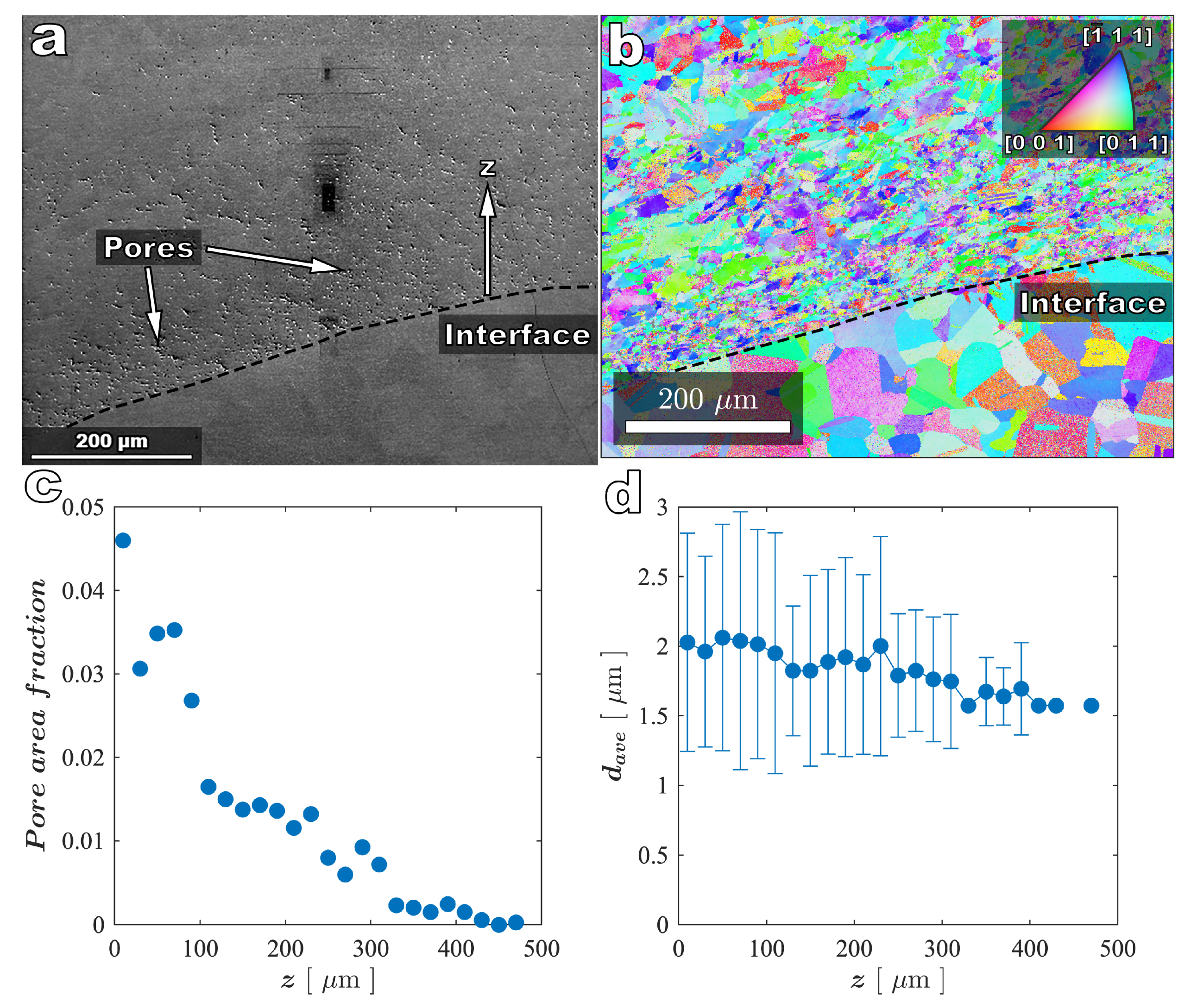
Figure 2 presents the scanning electron microscope results for our investigation of this porosity at the deposit edge (see the
Figure 3 for validation of these defects as pores).
Figure 2a, a secondary electron image, reveals this porosity present near the substrate–deposit interface as black spots.
Figure 2b, an inverse pole figure map of approximately the same region as (a), shows that there is an abrupt change in grain size across the deposit–substrate interface.
Figure 2c indicates that the pore area fraction decreases with distance from the interface (
z).
Figure 2d displays the average pore size as a function of distance from the interface. These results indicate that there is a small decrease in average pore size with increasing distance from the interface. The reason for such behavior will be described in more detail in the Discussion section.
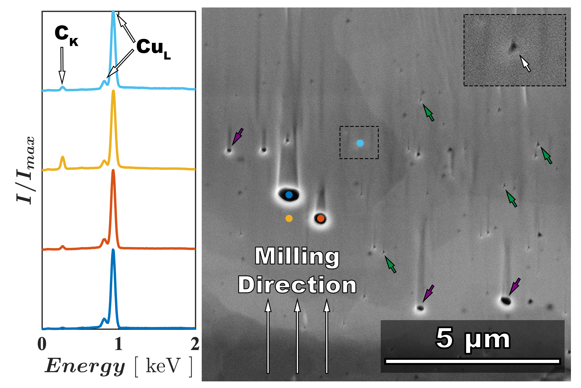
Though pores could be attributed to oxide pull out during mechanical polishing, this was confirmed not to be the case,
Figure 3. Using a focused ion beam (FIB), a trench was milled to reveal the nature of the defects. Since the ion milling directly cuts the material, pull-out of inclusions is mitigated. The milled surface reveals the porous structure, which enabled EDS point scans of these defects as well as the matrix. These results indicate that the only elements present are Cu and a small amount of C present (no O signal). The EDS scans are truncated in energy in order to effectively differentiate the Cu and C peaks at low energy; the higher energy portions of the spectra only have the Cu
K peaks. The O
K peak, if it were present, would occur at approximately 0.5 keV. The detection of C via EDS indicates some retention of the graphite lubricant coating applied to the feedstock prior to deposition.
The porosity was limited to the substrate–deposit interface region, i.e., porosity was not present in the deposit bulk. The rest of the results will focus on characterizing the bulk deposit’s microstructural and mechanical properties.
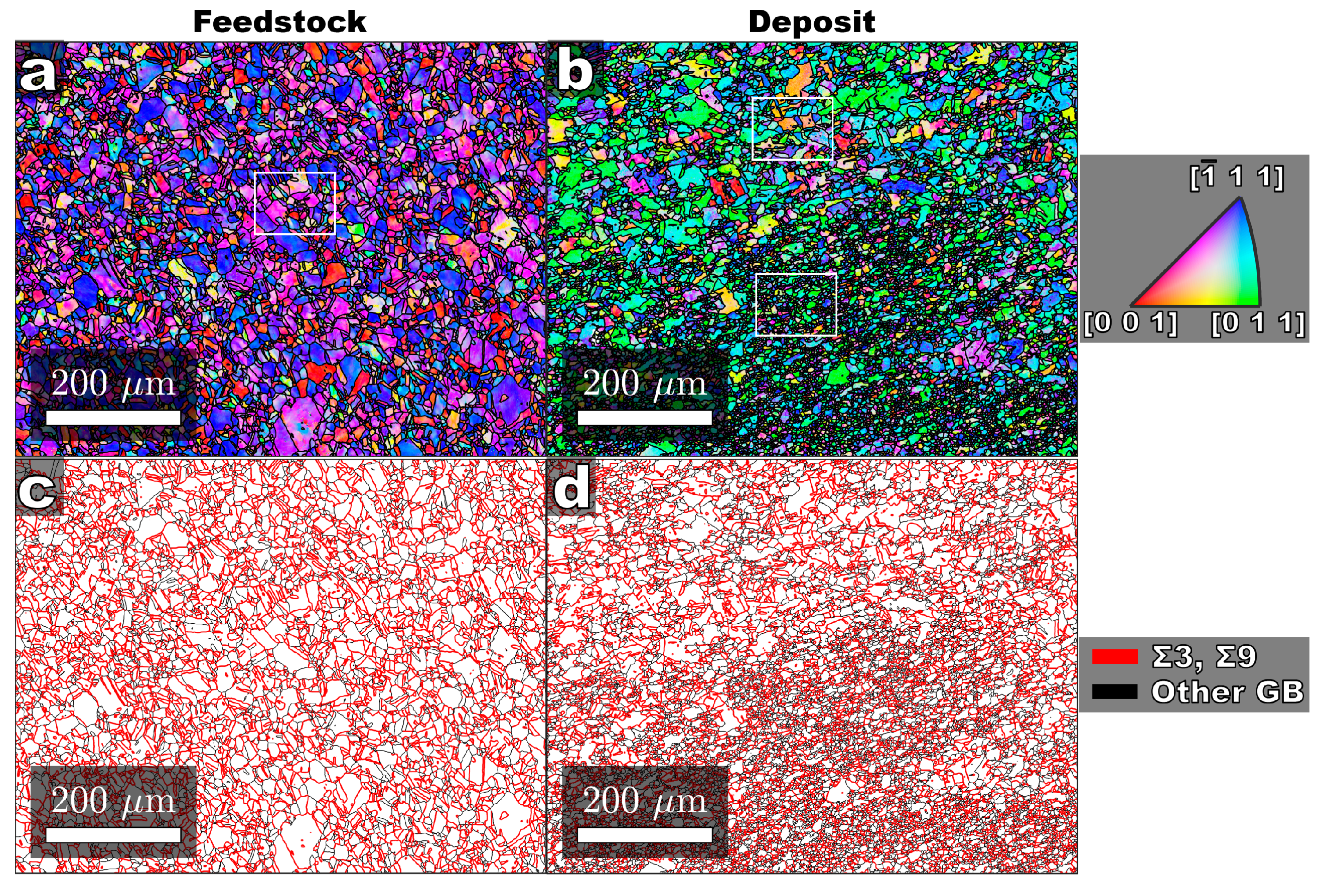
Table 1 summarizes the material attributes measured in this study, namely, the grain size, the twin fraction, and the Vickers microhardness. Low (e.g., 150×) and high (e.g., 1000×) nominal scanning electron microscope capture magnifications were used to ensure that the microstructural characteristics were simultaneously representative of the larger sample and accurately examined. These nominal capture magnifications are used to distinguish between “large” (low magnification) and “small” (high magnification) EBSD maps and are not meant to convey actual magnifications of the maps in this article. The reader is referred to the scale bars included with each map. Use of low/high magnifications and scan collection parameters contributes to slight differences in the resolved grain sizes. The summary table indicates that, at the center of the deposit, the average grain size and twin fraction decrease compared to the feedstock. The grains were also noted to be in a bimodal distribution (
Figure 4b). At the outer edge of the deposit (
Figure 1c), the grains also exhibited a bimodal distribution (
Figure 5) with a higher twin density than the center region. The average hardness decreased between the feedstock and all regions of the deposit.
The microstructures of the feedstock and the deposit center are surveyed (at 150×) with EBSD in
Figure 4a,b. Each scan used the same collection parameters and conditions to facilitate comparison between the resulting inverse pole figure maps. Visual inspection (
Figure 4a,b) and grain size analysis (
Table 1) indicate that deposition refines the grains, as observed in other materials [
7,
8,
9,
10]. Furthermore, the grain size refinement is not uniform throughout the deposit, with variance in the grain size depending on position within the deposit, as observed in Ref. [
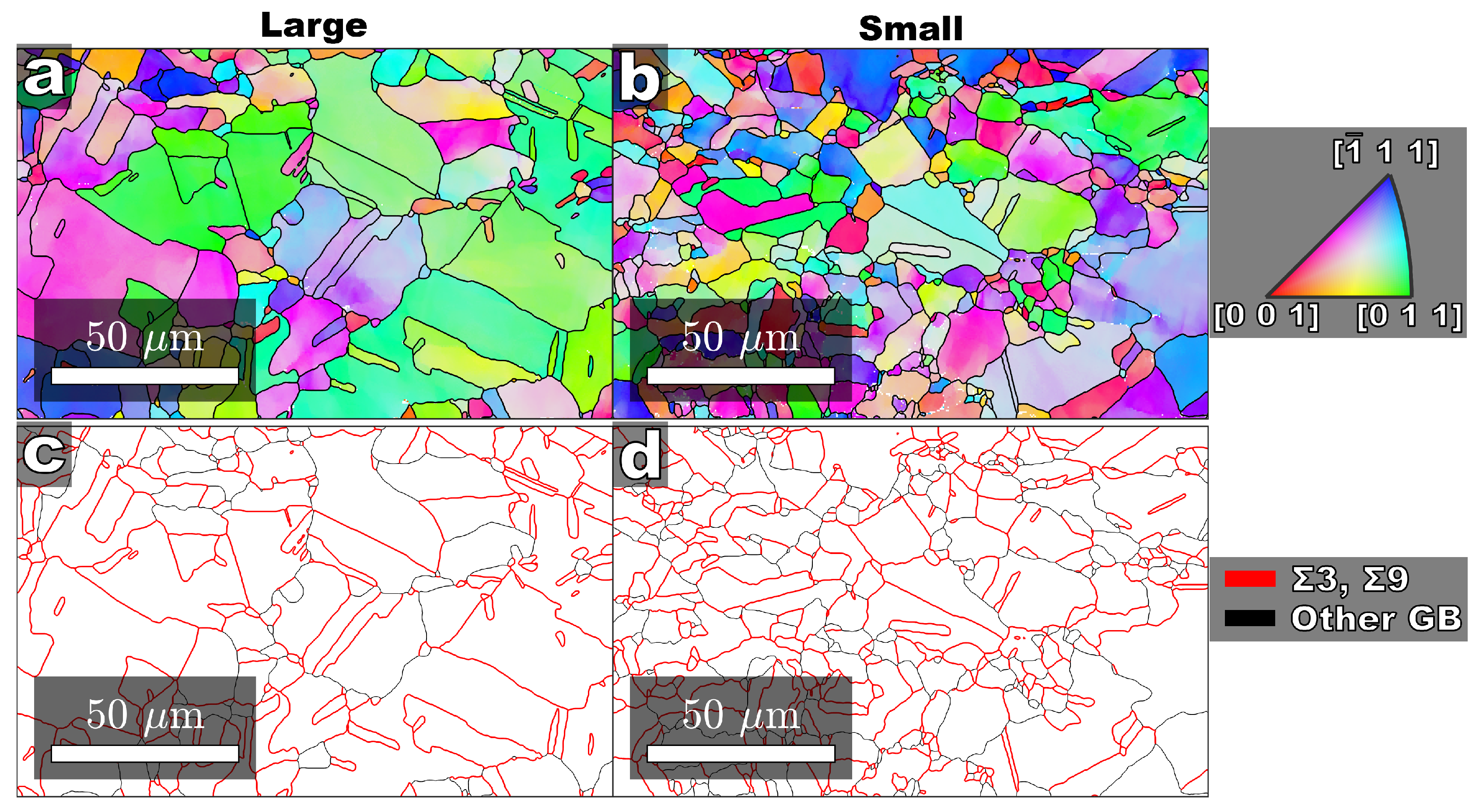
7]. To confirm the “survey” EBSD maps, we also conducted some EBSD scans at 1000× (
Figure 4c–h). As the grain size was observed to be uniform from the feedstock EBSD survey scan, we only conducted one such 1000× scan for the feedstock,
Figure 4c,f. For the deposit center, two 1000× scans were done in order to examine the largest (
Figure 4d,g) and smallest (
Figure 4e,h) grain size regions. For these 1000× scans, we plot an inverse pole figure map (
Figure 4c–e) and a map of the twin/non-twin grain boundaries (
Figure 4f–h) for each scan. The corresponding legends are found to the right of each row. In
Appendix B, we plot the two types of maps, following
Figure 4c–h, for the “survey” scans for completeness. The edge-of-the-deposit EBSD scans are shown in
Figure 5. These were conducted at 800× magnification in order to adequately characterize the slightly larger average grain size at the edge. Similar to the deposit center, there are regions of larger and smaller grains at the edge.
The textures of the feedstock and the deposit center are examined in
Figure 6. From these pole figures, the feedstock has a near
texture. While the deposit has a strong pole near
, it does not appear to have a well defined texture otherwise.
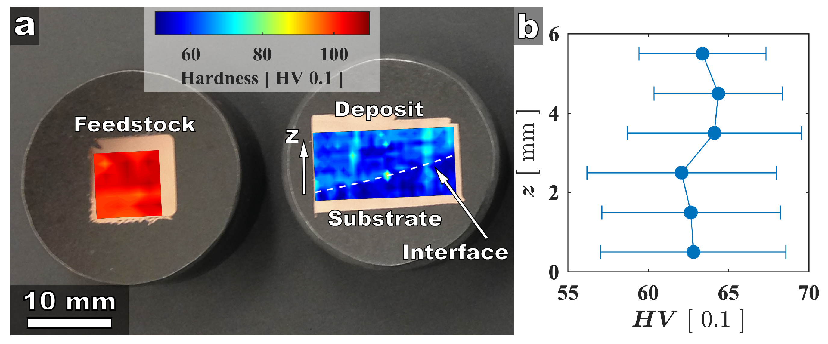
The Vickers hardness maps for the feedstock and the deposit are displayed in
Figure 7a. The colorbar used to denote hardness is the same between both conditions. Cool colors, such as blue and green, are lower hardness than warm colors (red and orange) which are higher hardness. The deposit, which is colored blue/green, has a lower hardness than the feedstock, colored red/orange.
Figure 7b plots the hardness as a function of distance from the interface, z (see also
Figure 2). From
Figure 7, there only appears to be a slight increase in hardness with distance from the interface, if there is any change at all.
From
Table 1 as well as
Figure 4 and
Figure 5, we observe a positive correlation between grain size and twin density in the microstructures, which is, as the average grain size increases, the twin density increases. A comparison of this result will be made to the literature in the discussion.
4. Discussion
The presence of O on the deposit exterior without detectable O content within the interior suggests that no shielding gas is necessary for protecting Cu from oxidation during the AFS-D process. Not only does this lower costs for operation, but it also simplifies the use of AFS-D for Cu repair applications in the field, where the proper application of shielding gas may be difficult to achieve. As four passes were achieved in the build, and no oxide scale is detected between layers, the outer “oxide shell” suggests that a kinetic aspect (longer exposure times) influences the accumulation of significant oxidation.
The bonding of the deposit to the substrate appears to be continuous along the cross section, although there is some porosity on the deposit side of the interface (observed from the center to the edge). The occurrence of this porosity is attributed to the lack of substrate surface preparation and/or the low initial deposition temperature, as the region of interest was deposited at the onset (on the unprepared substrate surface) when the tool had not yet reached the (higher) steady-state deposition temperature. This is in agreement with Polar and Indacochea (at least with respect to thermal conditions), who reported defect formation in friction stir welded Cu when the processing temperature was too low (initially). These defects did not appear once the processing temperature was sufficiently high later in the weld [
35]. They attributed the defects to insufficiently plasticized material at the lower temperature. The similarity of these published findings to our conditions suggests that low initial deposition temperature may have impeded material flow causing localized pore formation. This conclusion is further reinforced by the lack of porosity between subsequent deposition layers. Another possible cause of the porosity may be substrate preparation. No sanding or polishing of the substrate material occurred, which may have led to the pores. Possible solutions to the initial porosity in Cu could be resolved by (1) pre-heating the tool and the substrate, (2) increasing the dwell time to achieve a higher initial deposition temperature, and/or (3) improving the surface finish of the substrate. These possibilities are the subject of future investigation. One notable difference of the pores here compared to Polar and Indacochea is the size. In our work, the pores are microscopic, whereas Polar and Indacochea reported macroscopic pores [
35]. Unlike friction stir welding, material is constantly being added during AFS-D processing; thus, the application of additional material would act to fill defects macroscopically leaving only microscopic defects behind.
The structure of the pores also reinforces the idea that their origin stems from plasticity. In
Figure 3, we observe both rounded pores and pores with three-fold symmetry (e.g., the inset in the upper right of
Figure 3). The round pores tend to be larger and the ’three-fold-symmetry’ pores smaller. It is the three-fold symmetry that is important:
planes in face centered cubic materials have three-fold symmetry and are the primary slip planes. This suggests the accumulation of damage on
planes, which initially coalesce to form small pores (with the corresponding three-fold symmetry) and eventually coarsen to form larger circular pores.
To complete the discussion of “manufacturing” defects, there is significant flash generated from the deposit. This may be indicative of an ‘overfed’ condition, in which the feedrate for the feedstock material is too high [
10]. Possible decreases in the feedrate for the input material would alleviate the generation of this excess flash. These manufacturing defects are studied as they impact applications of AFS-D. For example, when used in repair, the potential for porosity may impact fatigue performance of the repaired component. Alternatively, the generation of flash impacts post-processing if the geometry of the final component is important.
While there is literature on the microstructures and/or properties resultant from friction stir welding of Cu [
35,
36], there is only one report known to the authors regarding AFS-D of Cu [
37], and that paper examines the thermal and material flow behaviors during deposition. Nevertheless, the hardness results presented in the present work agree with the literature on the friction stir welding of Cu, where the hardness values we report for the feedstock and the deposit (102 and 63 HV) correspond to the values reported for the base metal (analogous to the feedstock) and the weld (which is compared to the deposit) in friction stir welding: 105–110 HV and 60–90 HV, respectfully [
36]. Furthermore, transmission electron microscopy, conducted by Lee and Jung, showed that the dislocation density of the stir-zone (analogous to the deposit) is also much lower than that of the base metal because the material within the stir-zone has recrystallized [
36]. This is in agreement with our finding of an entirely recrystallized deposit, given the loss of feedstock texture (
Figure 6). As an aside, we note that the substrate has approximately the same hardness as the deposit, despite the larger grain size in the substrate. Nevertheless, the grain sizes of both regions are larger than the grain size range at which Hall–Petch becomes a dominant mechanism. A simple Hall–Petch calculation estimates the change in strength to be approximately 20 MPa between substrate and deposit.
The only very slight apparent increase in hardness of the deposited material with increasing distance from the deposit–substrate interface agrees very well with a similar findings in Refs. [
9,
23]. Although those works studied different material systems (2219 Al-based and WE43 Mg-based alloys, respectively), they observed only a slight increase in hardness with respect to build height (analogous to distance from the interface). As both River et al. and McClelland et al. note, when considering the error bars, there is little significant change in hardness across the height of the sample [
9,
23]. Such commentary is applicable to the results of this work as well, and suggests that AFS-D, as a technique, produces deposits with little variation in hardness. Further work exploring other systems and deposit geometries (e.g., taller deposit tracks) will be necessary to explore this interpretation.
The recrystallization behavior is important for several reasons. First, recrystallization relieves the excess energy associated with high microstructural defect densities (especially dislocations). Without additional plastic deformation, the dislocation density in the recrystallized material will be lower, decreasing the contribution of work hardening to the strengthening of the additive friction stir-deposited Cu. Lee and Jung attribute lower hardness of their friction stir welded Cu to the recrystallization that lowered the dislocation density [
36]. The deposited material has a generally refined grain size (except near the edge), which provides limited Hall–Petch-type strengthening (less than 20 MPa). Despite this predicted strengthening, the deposit is still softer than the work-hardened feedstock, which we attribute to the loss of high dislocation density as a result of recrystallization. From this result, work-hardening must be the more dominant strengthening effect for Cu at this grain size range.
The extent of recrystallization depends upon the temperature history of the material. Although the thermal behavior of the Cu during deposition was not recorded in the present study, work by Garcia et al. in the AFS-D processing of Cu provides a ready comparison [
37]. The processing conditions used by this paper and Garcia et al. are similar, with rotational speeds of 275 vs. 300 RPM, respectively, and traversing speeds of 2.12 mm/s and 2 mm/s, respectively. The conditions used by Garcia et al. produced a peak temperature in excess of 750 °C (0.7 T
M), with an exposure time (which they define by the full-width half-maximum peak value) of approximately 15
. For comparison, Blaz et al. report full recrystallization of a copper specimen tested in quasi-static (strain rate ∼2 × 10
−3s
−1 compression at 500 °C (0.46 T
M) [
32]. Based upon the higher temperature of Garcia et al., it is reasonable to conclude that full, or near full, recrystallization occurred in our Cu sample during deposition. This conclusion is bolstered by the refined, equiaxed grain structures observed in
Figure 4.
Second, recrystallization influences the formation of twins [
32], with dynamic recrystallization reportedly acting to suppress twins. From the EBSD examinations of this work, we have characterized the relative prevalence of twins as well as the grain size in the scanned regions. The twin content appears to depend on the local grain size, with larger local grain sizes corresponding to higher twin densities (
Table 1). In contrast, Blaz et al. conclude that twin density
decreases with increasing grain size in specimens tested in compression at elevated temperature [
32]. In conducting their investigation, Blaz et al. used optical microscopy—rather than EBSD—to characterize the grain boundaries in their material (optical microscopy may not see or properly identify twins). They also report this relationship for statically recrystallized specimens. Our sample, however, was subjected to a complex thermomechanical condition of AFS-D. EBSD improves our ability to resolve twin misorientations between “parent” grains, while still detecting the majority of twins that bifurcate a parent grain (parallel bands). By visual inspection, the parallel band twins occur with greater prevalence in the microstructures with coarser grains compared to those with finer grains. Therefore, the direct relationship between twin prevalence and grain size that we observe still holds. We attribute the differences in twin prevalence and grain size to the dynamic (rather than static) recrystallization under a complex thermomechanical condition that influences the AFS-D microstructures [
32].
Twin formation during recrystallization is important as it influences strength. However, the twins in the deposit do not appear to play a dominant strengthening role. This may have several causes. First, since EBSD does not completely define the grain boundary plane inclination when producing a two-dimensional map, we do not differentiate between coherent and incoherent twins. It may be that the deposit has more incoherent twins, which may or may not play a strengthening role. Second, many papers discussing the strengthening mechanisms of twins do so in the context of ‘nanoscale’ twins (twins with spacing of less than several hundred nanometers) [
25,
26], which was not achieved here (in either feedstock or deposit). It is true that EBSD and other scanning electron microscopy techniques have a resolution limit of approximately several hundred nanometers. However, the inclination of stacking faults to the polished surface can result in detection of those faults (like twins) even if the separation is less than a micrometer [
38]. Since no stacking fault structures (like those captured in Ref. [
38]) are evident in this case, we conclude that nanoscale twins are not present and thus do not represent a dominant strengthening mechanism in AFS-D Cu with the processing conditions employed.
Finally, recrystallization changes the texture in the material. The Cu feedstock was supplied in a cold-worked condition, which is known to produce a fiber texture in the resultant components (
Figure 6). The stirring and recrystallization of AFS-D result in a loss of this feedstock texture,
Figure 6, and cold-work-based strength is lost (
Figure 7).
To close the discussion, AFS-D processing of Cu yields a softer deposit than our feedstock material largely contributed to recrystallization, which is known to reduce dislocation density and produce a softer material. As the AFS-D process drives Cu to a lower dislocation density, there is a loss of work hardening that the refined grain sizes and/or higher twin densities in the deposit do not appear to effectively offset. In short, work hardening appears to be the dominant strengthening mechanism in this material state, but its efficacy is reduced because of the recrystallization induced by AFS-D. By manipulating the deposition parameters (e.g., rotational speed, traverse rate), future work may change the heat input history (temperature and time) and/or deformation characteristics so as to impact recrystallization. In this manner, it may be possible to achieve microstructures that limit the loss of strength associated with deposition and recrystallization of Cu as reported in this study.

