Article

Investigation of the Layer Effects Formed by W-EDM on Electrochemical Grooving of Stellite 21

1
Samsun Yurt Savunma, Samsun 55300, Turkey
2
Department of Mechanical Engineering, Engineering Faculty, University of Samsun, Samsun 55420, Turkey
*
Author to whom correspondence should be addressed.
Machines 2023, 11(8), 823; https://doi.org/10.3390/machines11080823
Submission received: 13 July 2023 / Revised: 26 July 2023 / Accepted: 1 August 2023 / Published: 10 August 2023
(This article belongs to the Special Issue Recent Advances in Surface Processing of Metals and Alloys)

Abstract

:
Machining hard-to-cut materials, such as cobalt (Co)-based superalloys, is a common problem in manufacturing industries. Background: wire electrical discharge machining (W-EDM) is one of the widely used cutting processes that causes layer (white layer—WL and heat-affected zone—HAZ) formation, and microcracks on the material’s surface. Purpose: this study investigates the effects of WL and HAZ on the electrochemical grooving (EC grooving) performance of Co-based superalloys. Two different surface types (W-EDMed and VFed) were used in the experiments. Result: the experiments showed that material removal rate (MRR) values increased up to 212.49% and 122.23% for vibratory finished (VFed) and wire-electrical-discharge-machined (W-EDMed) surfaces, respectively. Conclusion: This result indicates the presence of HAZ and WL that prevent current transition between two electrodes. However, increased voltage causes an increase in surface roughness, with increment rates at 71.13% and 36.08% for VFed and W-EDMed surfaces, respectively. Moreover, for the VFed surfaces, the groove lost its flatness at the bottom after an approximately 100 µm depth due to the different electrochemical machineabilities of HAZ and real surface texture. This result can be attributed to the different microstructures (HAZ and surface texture) showing different electrochemical dissolution rates. Therefore, high-depth distance HAZ and WL must be removed from the workpiece.

1. Introduction

Cobalt (Co)-based superalloys are used in defense, biomedical, and aerospace industries for high-temperature applications due to superior mechanical properties and high oxidation resistance. Stellite 21 is the Co-based superalloy composed of a Co matrix with chromium (Cr), tungsten (W), molybdenum (Mo), and carbon (C). Machining Stellite 21 through conventional machining processes can cause unpredictable defects, such as microcracks and thermal and mechanical stresses, on the workpiece surface. Therefore, nonconventional machining processes stand out for this type of hard-to-machine materials.
Electrical discharge machining (EDM), which does not use any load and force when machining materials, is commonly used to process hard-to-machine metals [1]. This method is one of the most widely used non-conventional techniques due to its magnificent advantages, such as low surface roughness and the ability to machine materials regardless of hardness. The material is ionized at high temperatures of between 800 °C and 1200 °C by a high-frequency voltage between the tool and the workpiece [2]. Then, the material melts and evaporation begin to form [3]. This phenomenon leads to problems such as thermal cracks, tool wear, residual stress, heat-affected zone (HAZ), and white layer (WL) affecting the mechanical properties of the workpiece [4]. Due to these disadvantages, the usability of EDM in automobile, aerospace, defense, and biomedical industries is limited [5]. During this process, the melted materials partly crystallize and are partly amorphous [6] after being cooled down by a non-conductive fluid, and a layer called the recast (white) layer is formed [7]. This layer shows different surface morphology from the original structure of the material [8]. It also causes changes in fatigue strength, corrosion resistance, surface morphology [9], and tool wear [10]. Certain methods, such as pico-second laser [11] and ultrasonic assisted and cryogenically cooled EDM [12], are used to remove the WL that is formed during EDM. However, these types of solutions are time consuming and costly.
Electrochemical grooving (EC grooving), which is one of the most familiar machining methods of electrochemical machining, is a non-traditional machining method that provides cost-effective machining of superalloys without tool wear, microcracks, and residual stresses. In EC grooving, the anodic dissolution depends on the principle of electrolytic processes. Hard-to-cut materials, such as Co- and nickel (Ni)-based superalloys, can be machined regardless of their mechanical properties. Zhao et al. [13] investigated the electrochemical dissolution behavior of Ni and Co alloys in a sodium nitrate (NaNO3) electrolyte solution. In Ni-based alloys, pits were formed in the material, whereas in Co-based materials, carbides that are insoluble on the surfaces consisted of grain limit and current density of dendrite regions. The interelectrode gap significantly affects the ECM process performance in terms of machining accuracy and surface quality [14]. Wang et al. [15] reported that with the increase of gap distance affects significantly the dimensional and roundness accuracy due to low localization. Wang et al. [14] proposed a novel technique that to realize a consistent gap distance with the use of visual assistance throughout ECM process. Voltage, a critical parameter in the ECM process, affects the surface roughness and quality. Xu et al. [16] reported that the voltage above 20 V causes a high amount of electrolyte dissolution, and therefore the surface quality for Ti60 alloys decreases. Additionally, the voltage increase adversely affects the machining width, and therefore the stray machining is dominant on the workpiece surface [17].
EC grooving and EDM are nonconventional machining processes that have advantages over each other. Although EDM has a higher material removal rate (MRR), lower surface roughness (Sa) is obtained with electrochemical machining (ECM) [18]. Specific studies revealed the advantages of these two methods while alleviating their adverse effects [19,20,21]. As reported by Nguyen et al. [20], ECM contributes to the removal of the WL and HAZ through electrochemical reactions. Furthermore, Sa is significantly reduced in electrical discharge machined (EDMed) surfaces by using ECM for lapping and complex shapes [22]. Steuer et al. [23] investigated the effect of HAZ on the machinability of copper-based alloys in pulsed ECM, but no visible change was observed. The specimens were used as a tool in EDM. Then, pulsed ECM was applied, and the surfaces around the specimens were machined.
In manufacturing, the number of processes affects productivity by increasing the time and costs of part production. Therefore, two different surfaces, applied and not applied with vibratory finishing (VF), are used in the experiments. The Co-based superalloy (Stellite 21) is cut by using wire EDM (W-EDM), and WL is removed through VF. The experiments were conducted simultaneously on the two types of surfaces, namely with WL (W-EDMed) and without WL (vibratory finished [VFed]). The effects of WL and HAZ on EC grooving are defined by MRR, groove profile geometry, taper angle, and Sa. The results showed that an increase in voltage and a decrease in gap distance increase the MRR for both surface types, but with a lower increment rate for W-EDMed surfaces as WL prevents current transition. Furthermore, groove flatness deteriorates after ~100 µm for VFed surfaces, showing that HAZ is an effective parameter on the groove geometry. Additionally, Sa increases with voltage for VFed surfaces but not with W-EDMed surfaces. Experimental results showed that EC grooving can be used without any additional finishing process after W-EDM.

2. Materials and Methods

The experiments used a recently developed desktop-sized EC grooving machine, with detailed information found in [24]. In this study, Stellite 21 and copper were used as the workpiece and tool material, respectively. Stellite 21 is the best-known cobalt-based superalloy with a combination of mechanical and tribological properties at both high and room temperature, and outstanding oxidation and corrosion resistance. Its strength is enhanced by the presence of solid solution forming elements such as Mo and Cr in its chemical composition. The chemical composition of Stellite 21 is checked by in-house spectrometry test (OE750, Hitachi, Japan, Tokyo). Table 1 presents the chemical composition and mechanical properties of Stellite 21.
Stellite 21 specimens were fabricated by sintering and were cut via W-EDM to investigate the effects of WL and HAZ on the EC grooving performance of the workpiece. VF was used to remove the WL on the surface. The specimen size is 25 mm3. Figure 1 presents photographs of the W-EDMed and VFed surfaces. The VFed parts are obtained by using a S-101/C 13 × 13 SC high abrasive materials after a 2 h process.
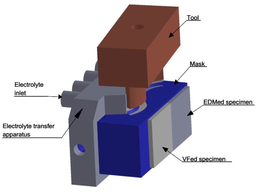
The cathode is S-shaped and produced via the copper material. The machined surfaces were masked to avoid stray current and thus decrease the groove length and taper angle. The mask material was polylactic acid (PLA), which is nonconductive and was fabricated via a 3D printer (Zhejiang Flashforge, Creator 3, China, Jinhua). Flashforge PLA was used as the apparatus material. The properties of PLA and apparatus is shown in Table 2.
A transfer apparatus fabricated of the PLA is designed for the transfer of the electrolyte to the machining area. Figure 2 illustrates the schematic of the specimens and the cathode.
EC grooving parameters, such as gap distance and voltage, were used to design the experimental conditions. Electrolyte conductivity, flow rate, electrolyte type, and machining time parameters were kept constant. The electrolyte type is NaCl and the electrolyte flow is controlled by a frequency inverter (ACS310, ABB, Zurich, Switzerland). The electrolyte temperature is checked by a thermal camera (Xi80, Optris, Berlin, Germany). The machining time significantly affects the MRR and surface roughness, but the works related to this parameter can be found in the literature [25,26], and therefore this parameter is constant at 65 s. Table 3 presents the experimental conditions and the constant parameters.
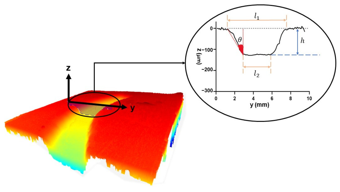
Surface roughness is used to evaluate the quality of a workpiece. It is one of the most important quality attributes of an EC grooving process. The effect of gap distance, voltage and surface type parameters shown in Table 3 on the surface roughness of EC grooved parts are also investigated. Therefore, the machined surface profile of the groove and Sa values were measured by a white light interferometer (Polytec TopMap Metro.Lab TMS 150, Berlin, Germany). The taper angle on the workpiece surface forms due to the stray current between the anode and the cathode in the EC grooving process. Thus, the taper angle of the S line is a significant criterion to estimate the quality of the EC grooved surface. The output parameters were determined by MRR, Sa, and taper angle of the groove profile to discuss the EC grooving performance of Stellite 21. The MRR and the taper angle are calculated as follows:
MRR = (mb − ma)/t,
θ = tan−1((l1 − l2)/2 h),
where mb and ma are the mass of the specimens before and after machining, respectively, t is the machining time, l1 and l2 are the top and bottom lengths, respectively, θ is the taper angle and h is the height of the EC grooving groove. The initial and final weights of the workpieces were taken by a precision electronic scale. The taper angle and groove geometry of the EC grooved surface is shown in Figure 3.
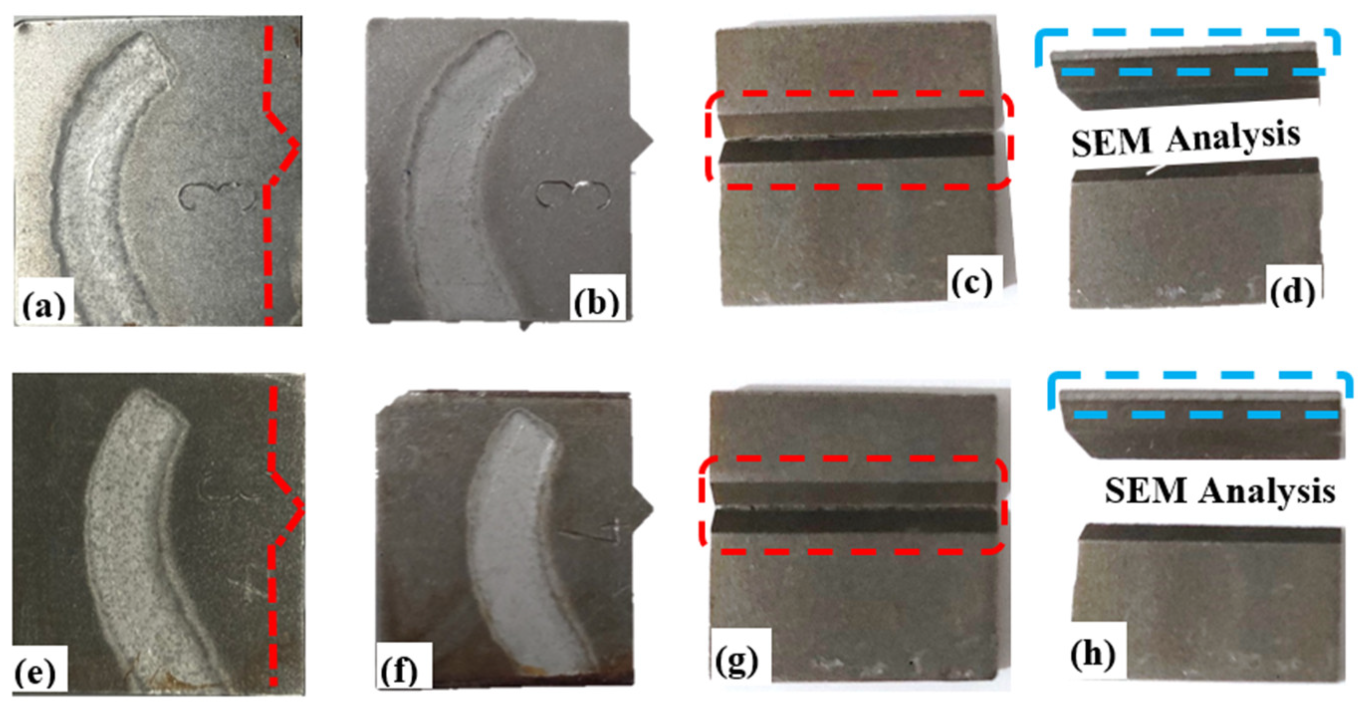
Figure 4 shows the preparation of the machined surface and substrate of the specimens for SEM analysis. The VFed and W-EDMed surfaces are shown in Figure 4a,e, respectively. These specimens were cut via the W-EDM machine as indicated by the red line (Figure 4a,e) in order to investigate the effect of EC grooving process on surface and substrate of the specimens. After cutting, the thin parts (Figure 4c,g) were fractured with a hammer and the parts were prepared for SEM analysis (Figure 4d,h). The blue line areas in Figure 4d,h were investigated with SEM.

3. Results

3.1. Analysis of MRR

Two different surface types (VFed and W-EDMed) were used in the experiment to investigate the effects of WL and HAZ on EC grooving performance. Figure 5 shows the variation in MRR for the two surface types at different gap values. According to Faraday’s laws, MRR can also be calculated by Equation (3):
MRR = (i·kv)/(F·ρa),
where i is the current density, kv is electrochemical machinability, F is the Faraday constant, and ρa is the density of the workpiece. For the same material (kv and ρa are constant), MRR varies with the current density, which is directly proportional to the voltage for the constant electrical conductivity or resistance. The reason is that the higher the voltage between the anode and the cathode during the EC grooving process, the higher the current density on the anode surface and causes more anode material to dissolve per unit time. As can be seen from Figure 5, there is a linear relationship between MRR and voltage.
The interelectrode gap and its width directly affect the machining accuracy, and therefore it is necessary to maintain the gap in the EC grooving for high machining accuracy [14]. Figure 6 shows the variation in MRR with a gap at variable voltage values. As seen from the figure, there is a linear dependence with a negative slope between gap and MRR. Similar results in regard to investigation of the relationship between gap and MRR can be found in the literature [14,27]. As is known, the current density increases at low IEG values as well as at high voltage values, thus increasing the MRR value. This is why the highest MRR for VFed is obtained at 20 V and 1 mm. However, the decrease in MRR is slower at later IEG values. This is due to both the decrease in current density and the bubble generation in the gap.
The amount of error of the VFed surface changes at a wide range for MRR. Therefore, the machining operation in the VFed surface was not properly performed compared with that in the W-EDMed surface. The variation in MRR is not effective at less than 20 V for the two surface types. However, more material was removed from the Vfed surface at 20 V. As mentioned above in Table 1, the workpiece composition contains high amounts of Co. As reported by Schneider et al. [28], an increase in overpotential causes an increase in the dissolution rate of Co from the workpiece. Choi et al. [29] investigated the electrochemical characteristic of tungsten carbide with the Co binder according to machining conditions. Grooves were investigated via EDX at the machined surface, and high amounts of Co and O elements were determined. Therefore, Choi et al. [29] proposed an idea that the Co oxide is generated on the groove surface and also suggested using an electrolyte capable of dissolving Co. WL is expected to play a mask role via the contained oxide films and prevent current transition between electrodes. Therefore, the standard deviation for the W-EDMed surface is closer to zero than that for the VFed surface. Thus, the MRR is more predictable for the W-EDMed surface.
In the graph, it can be seen that VFed specimens have higher MRR at lower gap distance and higher voltage. This is illustrated schematically in Figure 7. Figure 7 shows the EC grooving process for the two surface types and the electric circuit diagram, where subscript “c” is the cathode, “E” is the electrolyte, “WL” is the white layer, “HAZ” is the heat affected zone, “A” is the anode, “R” is the resistance, and “C” is the capacitor of the circuit element.
Electrolyte conductivity can be calculated as follows:
k = l/AR,
where k is the electrolyte conductivity, l is the gap distance, and A is the cross-sectional area. According to Ohm’s law, k can be obtained in Equation (5):
k = l·i/V,
where V is the voltage and substitution of Equation (5) into Equation (3). Therefore, MRR can be calculated by Equation (6):
MRR = (k·V·kv)/(F·l·ρa).
Equation (6) above shows that the gap increases negatively affect the MRR, thus confirming the experimental results.
Figure 8 shows the SEM analysis of the W-EDMed and VFed surfaces. The two surfaces differ in brightness due to the removal of the WL at W-EDM. WL contains weakly bonded oxide films as illustrated in Figure 8a,b. As shown in the graph in Figure 5, the MRR value is higher for the Vfed specimens and can be attributed to the bond structures shown in Figure 8. In Figure 8d, the VFed surface with the removal of WL pores and melted layers (light blue) via the sintering and W-EDM is clearly visible. The pores and the boundary that appear in the workpiece indicate the grain and grain boundary, respectively, caused by the phase differences between the powders. In the W-EDM process, the powders on the surface are welded together and tend to fill the pores. The filled pore is shown in Figure 8b. The VFed surface (Figure 8c,d) is more clear and homogenous than W-EDM due to non-WL. Furthermore, unlike the W-EDMed surface, the pore in Figure 8d is not filled.

3.2. Analysis of Surface Roughness and Groove Profile

In this section, Sa and groove profile results and the effect of the EC grooving parameters on these results are discussed. Figure 9 illustrates the effect of voltage on Sa for VFed and W-EDMed surfaces graphs. As seen in Figure 9a and Figure 10a, for the VFed surface, the increase in gap distance increases the voltage, negatively affecting Sa, whereas the case is the opposite in the W-EDMed surface. In addition, Sa does not significantly change at lower gap distances. Sa variation shows similarity to the results in the literature on the VFed workpiece [30]. However, the WL that is not removed from the W-EDMed surface is highly effective on Sa.
Figure 10 shows the graph of the effect of gap distance on Sa. The results show that the increasing pattern in gap distance negatively affects Sa, and this change becomes linear at 20 V. However, a higher Sa value was obtained at 10 V for the W-EDMed surface. The increment rate of Sa is 71.13% and 36.08% for the VFed and W-EDMed surfaces, respectively.
Figure 6 and Figure 10 show that the increase in MRR causes an increase in Sa for the VFed surface, whereas the case to the opposite in the W-EDMed surface. These results show that HAZ also has an important role in Sa. HAZ can be formed after W-EDM, and as reported by Shabgard et al. [31], it is softer than other layers and can contain microcracks. In addition, it can cause the development of stress fractures resulting in minor and catastrophic failures due to the weakening of the material. Therefore, the variation in Sa is related to the microcracks and stress fractures at different layers. In the current study, the HAZ layer was removed from the workpiece, and then the main surface texture was machined at a higher MRR. As discussed above, HAZ and surface texture show different microstructures. This condition can cause different electrochemical machinabilities that prevent uniform machining. Thus, the electrolyte forms turbulence flow in the machined groove. However, the opposite is observed for the W-EDMed surfaces. Therefore, the HAZ layer is not removed efficiently.
The highest Sa values are obtained for the W-EDMed surface at the lowest (10 V) voltage and highest gap distance (1.5 mm). As presented in Equation (6), the lowest MRR is obtained at these experimental conditions. Therefore, the measured area has a heterogeneous structure containing WL, that is, the melted layer (Figure 8), which can be the reason for this result. However, the graph (Figure 9b) shows that voltage is not highly effective on Sa. The increment in Sa is higher for the VFed surface at different gap distances, indicating that regular machining cannot be performed properly. Similar results are obtained for voltage (Figure 9b), and the effect of HAZ and surface texture can be seen clearly at 20 V, with the highest MRR.
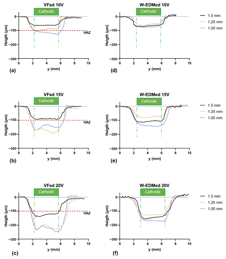
Figure 11 shows the groove profiles for the two surface types machined with different EC grooving parameters. Profile geometry is measured by a white light interferometer as described in Figure 3. The 3.5 mm wide cathode is shown in green and the width is indicated by a green dashed line. In Figure 11, the groove bottom becomes a non-linear geometry for the VFed surface after approximately 100 µm. As depicted in Figure 6a, with an increase in MRR, the HAZ layer is removed, and the real surface texture is exposed. As discussed above, via the turbulence flow, different structures of the material that cannot be removed cause geometrical errors. However, the groove bottom is almost linear for the W-EDMed surface. Thus, this result can be attributed to the WL that obstructs the current transition in a limited time, resulting in less machining time left to remove the HAZ layer that is not removed properly. The lowest depth is obtained at Figure 11a,d due to the lowest voltage level. However, for the VFed and the W-EDMed surface at a 1 mm gap, the depth is 112.13 mm and 87.62 mm, respectively. The most crucial parameter for this situation is the presence of WL on the surface. The groove bottom for Figure 11b,c is shaped as “M”. This situation can be attributed to the current density on the cathode surface. It is thought that an “M”-shaped machining can occur as a result of the decrease in the current density towards the center where the current density is high at the sharp corners of the cathode. For W-EDMed surfaces, the increase in depth as the voltage increases is a natural phenomenon. However, it has been observed that the depth increases more rapidly from 15 V to 20 V. This is thought to be due to the partial removal of WL.
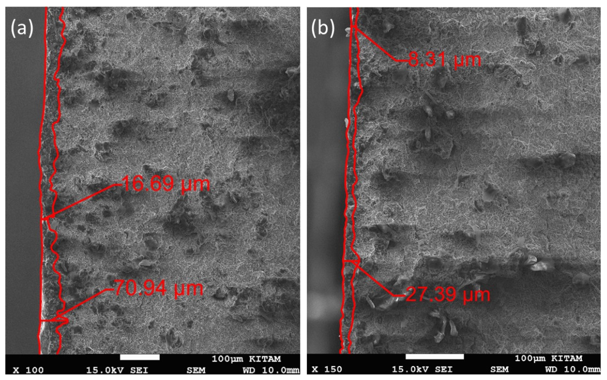
Figure 12 illustrates the backscattered electron images of the cross-sections for further analysis of the effect of HAZ on the groove profile after the EC grooving at 15 V, 1.5 mm experimental condition. In Figure 12a, the HAZ layer is thicker for the W-EDMed surface, varying between 16.69 µm and 70.94 µm. However, the lowest (8.31 µm) and highest thickness (27.39 µm) values are less between 50.21% and 61.39%, respectively, for the VFed specimens.
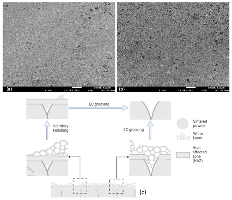
Additionally, Figure 13 shows the SEM images for the VFed+ EC grooved specimens for the same gap distances and different voltages. Pores and crevices are clearly visible at the 15 V EC grooving, resulting in a lower MRR (Figure 5a) than in the 20 V experimental condition. This finding confirms the results presented in Figure 11b,c (black-colored groove profiles).
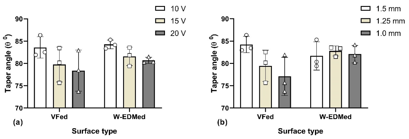
It is well known that the taper angle is one of the most important criteria in EC grooving in terms of surface and hole quality [32]. Stray electric field and stray corrosion are known to cause taper angle and affect surface texture [33]. Figure 14 shows the mean and standard deviation of the taper angles of the specimens calculated in Equation (2). Voltage increases cause a decrease in taper angle for the two surface types, indicating that the geometric accuracy increases. Moreover, the range of standard deviation of the taper angle is extremely high for the VFed surface. Additionally, the lowest taper angle (77.23°) is obtained at a 1 mm gap distance, and similar standard deviation ranges are obtained as presented in Figure 14b for the VFed surface. However, for the W-EDMed surface, the mean of the taper angle does not significantly change at different gap distances. The WL on the surface acts like a mask and prevents electron transfer around the groove. Therefore, the length of the groove is decreased significantly.

4. Conclusions

Co-based superalloys have critical roles in the manufacturing industries, such as defense, biomedical, and aerospace. Disadvantages such as tool wear, residual stress formation, and low surface quality limit the conventional machining processes for these types of materials. W-EDM processing is a non-traditional method; however, the method can cause different layers, such as WL and HAZ, in the workpiece surface. These layers affect the machining performance and mechanical behavior of the workpiece. It is well known that the VF is commonly used to remove WL. The HAZ and WL structures or their mechanical behaviors have been studied; however, few research can be found regarding their effects on MRR and surface roughness in the literature. Moreover, little research can be found on non-traditional machining method in the literature on Stellite 21. Therefore, in this study, machining surfaces with and without WL were investigated to reduce the number of steps in the EC grooving process. The primary experimental results are summarized as follows:
  • Variation in MRR with voltage and gap distance shows a similarity to the results in literature on both surface types.
  • Higher MRR values obtained for the VFed specimens show that the WL acts as a circuit element and decreases current efficiency. Also, in the W-EDMed surfaces, MRR is more predictable than in the VFed surfaces as the change in variation is lower (Figure 8).
  • The effect of voltage on Sa for W-EDMed surfaces is unclear, whereas it increases Sa in VFed surfaces, particularly at the highest gap distance. This result shows that the WL has an effective role in the surface integrity of the EC grooved grooves.
  • The HAZ thicknesses in VFed parts are 50.21% and 61.39% less than in the W-EDMed parts, with the lowest and highest layer thickness values.
  • At the highest voltage (20 V), the increment rate of Sa is 71.13% and 36.08% for the VFed and W-EDMed surfaces, respectively.
  • As seen from the groove profiles (Figure 13), after approximately 100 µm, the groove loses its flatness at the bottom for the VFed surfaces. This result shows that after removing the HAZ layer via the different electrochemical dissolution rates (HAZ and surface texture), turbulence occurs in the groove. However, for the W-EDMed surfaces, the depth of the groove increases up to approximately 180 µm, and the flatness does not change substantially. This result can be attributed to the WL thickness that prevents current transition, leading to the non-removal of the HAZ layer from the machining area.
  • Increases in voltage cause a decrease in taper angle for both surface types, but the range of variation is higher for the VFed surface, which is similar to MRR.

Author Contributions

S.E.A.: Methodology, Investigation; H.D.: Supervision, Visualization, Writing and editing, Conceptualization; A.K.: Writing, Original Draft and Methodology; A.C.: Writing, Editing and Investigation. All authors have read and agreed to the published version of the manuscript.

Funding

This study was funded by Defence Industry Agency, Presidency of the Republic of Turkiye (grant number 20SC017).

Data Availability Statement

The data presented in this study are available on request from the corresponding author.

Acknowledgments

The authors would like to thank “Incekaralar Inc., Turkey, Ankara” for the optical measurements. Figure 7 and Figure 13 are created with BioRender.com.

Conflicts of Interest

The authors declare no conflict of interest. The funders had no role in the design of the study, the collection, analyses, or interpretation of data, the writing of the manuscript, or the decision to publish the results.

References

  1. Ablyaz, T.R.; Shlykov, E.S.; Muratov, K.R.; Osinnikov, I.V.; Bannikov, M.V.; Sidhu, S.S. Investigation of Plasma-Electrolytic Processing on EDMed Austenitic Steels. Materials 2023, 16, 4127. [Google Scholar] [CrossRef] [PubMed]
  2. Fonda, P.; Nakamoto, K.; Heidari, A.; Yang, H.-A.; Horsley, D.; Lin, L.; Yamazaki, K. A Study on the Optimal Fabrication Method for Micro-Scale Gyroscopes Using a Hybrid Process Consisting of Electric Discharge Machining, Chemical Etching or Micro-Mechanical Milling. CIRP Ann. 2013, 62, 183–186. [Google Scholar] [CrossRef]
  3. Mohd Abbas, N.; Solomon, D.G.; Fuad Bahari, M. A Review on Current Research Trends in Electrical Discharge Machining (EDM). Int. J. Mach. Tools Manuf. 2007, 47, 1214–1228. [Google Scholar] [CrossRef]
  4. Hsue, A.W.; Huang, Z.-Y. Deionized Water Electrochemical Machining Hybridized with Alumina Powder Polishing for Microcavity of M-333 Mold Steel. Processes 2022, 10, 152. [Google Scholar] [CrossRef]
  5. Wu, X.; Li, S.; Jia, Z.; Xin, B.; Yin, X. Using WECM to Remove the Recast Layer and Reduce the Surface Roughness of WEDM Surface. J. Mater. Process. Technol. 2019, 268, 140–148. [Google Scholar] [CrossRef]
  6. Klocke, F.; Hensgen, L.; Klink, A.; Ehle, L.; Schwedt, A. Structure and Composition of the White Layer in the Wire-EDM Process. Procedia CIRP 2016, 42, 673–678. [Google Scholar] [CrossRef]
  7. Azam, M.; Jahanzaib, M.; Abbasi, J.A.; Abbas, M.; Wasim, A.; Hussain, S. Parametric Analysis of Recast Layer Formation in Wire-Cut EDM of HSLA Steel. Int. J. Adv. Manuf. Technol. 2016, 87, 713–722. [Google Scholar] [CrossRef]
  8. Han, Y.; Liu, Z.; Cao, Z.; Kong, L.; Qiu, M. Mechanism Study of the Combined Process of Electrical Discharge Machining Ablation and Electrochemical Machining in Aerosol Dielectric. J. Mater. Process. Technol. 2018, 254, 221–228. [Google Scholar] [CrossRef]
  9. Ayesta, I.; Izquierdo, B.; Flaño, O.; Sánchez, J.A.; Albizuri, J.; Avilés, R. Influence of the WEDM Process on the Fatigue Behavior of Inconel® 718. Int. J. Fatigue 2016, 92, 220–233. [Google Scholar] [CrossRef]
  10. Wu, S.; Liu, G.; Zhang, W.; Chen, W.; Wang, C. Formation Mechanism of White Layer in the High-Speed Cutting of Hardened Steel under Cryogenic Liquid Nitrogen Cooling. J. Mater. Process. Technol. 2022, 302, 117469. [Google Scholar] [CrossRef]
  11. Wälder, G.; Richard, J. Removal of the Heat Affect Zone Created by EDM with Pico-Second LASER Machining. Procedia CIRP 2016, 42, 475–480. [Google Scholar] [CrossRef]
  12. Srivastava, V.; Pandey, P.M. Study of Ultrasonic Assisted Cryogenically Cooled EDM Process Using Sintered (Cu-TiC) Tooltip. J. Manuf. Process. 2013, 15, 158–166. [Google Scholar] [CrossRef]
  13. Zhao, L.; Zhang, Y.; Bian, H.; Wang, G.; Ji, L. Investigation of Electrochemical Dissolution Behavior of Ni(γ)/Ni3Al(γ’) and Co(γ)/Co3Al(γ’) Superalloys in NaNO3 Solution. Corros. Sci. 2022, 208, 110622. [Google Scholar] [CrossRef]
  14. Wang, J.; Xu, Z.; Liu, J.; Tang, X. Real-Time Vision-Assisted Electrochemical Machining with Constant Inter-Electrode Gap. J. Manuf. Process. 2021, 71, 384–397. [Google Scholar] [CrossRef]
  15. Wang, D.; Li, J.; He, B.; Zhu, D. Analysis and Control of Inter-Electrode Gap during Leveling Process in Counter-Rotating Electrochemical Machining. Chin. J. Aeronaut. 2019, 32, 2557–2565. [Google Scholar] [CrossRef]
  16. Xu, Z.; Chen, X.; Zhou, Z.; Qin, P.; Zhu, D. Electrochemical Machining of High-Temperature Titanium Alloy Ti60. Procedia CIRP 2016, 42, 125–130. [Google Scholar] [CrossRef]
  17. Anasane, S.S.; Bhattacharyya, B. Experimental Investigation into Micromilling of Microgrooves on Titanium by Electrochemical Micromachining. J. Manuf. Process. 2017, 28, 285–294. [Google Scholar] [CrossRef]
  18. Klocke, F.; Zeis, M.; Klink, A.; Veselovac, D. Technological and Economical Comparison of Roughing Strategies via Milling, Sinking-EDM, Wire-EDM and ECM for Titanium- and Nickel-Based Blisks. CIRP J. Manuf. Sci. Technol. 2013, 6, 198–203. [Google Scholar] [CrossRef]
  19. Kurita, T.; Hattori, M. Development of New-Concept Desk Top Size Machine Tool. Int. J. Mach. Tools Manuf. 2005, 45, 959–965. [Google Scholar] [CrossRef]
  20. Nguyen, M.D.; Rahman, M.; Wong, Y.S. Simultaneous Micro-EDM and Micro-ECM in Low-Resistivity Deionized Water. Int. J. Mach. Tools Manuf. 2012, 54–55, 55–65. [Google Scholar] [CrossRef]
  21. Skoczypiec, S.; Ruszaj, A. A Sequential Electrochemical-Electrodischarge Process for Micropart Manufacturing. Precis. Eng. 2014, 38, 680–690. [Google Scholar] [CrossRef]
  22. Kurita, T.; Hattori, M. A Study of EDM and ECM/ECM-Lapping Complex Machining Technology. Int. J. Mach. Tools Manuf. 2006, 46, 1804–1810. [Google Scholar] [CrossRef]
  23. Steuer, P.; Rebschläger, A.; Weber, O.; Bähre, D. The Heat-Affected Zone in EDM and Its Influence on a Following PECM Process. Procedia CIRP 2014, 13, 276–281. [Google Scholar] [CrossRef] [Green Version]
  24. Demirtas, H.; Yilmaz, O.; Kanber, B. Development of a Desktop Size Electrochemical Machine for Micro/Macro Manufacturing. In Proceedings of the International Conference on Machine Design and Production, Bursa, Turkiye, 12–15 July 2016. [Google Scholar]
  25. Wang, D.; Yu, J.; Le, H.; Zhu, D. Localized Sinking Electrochemical Machining of Pre-Shaped Convex Structure on Revolution Surface Using Specifically Designed Cathode Tool. J. Manuf. Process. 2023, 99, 605–617. [Google Scholar] [CrossRef]
  26. Schaarschmidt, I.; Luther, F.; Steinert, P.; Richter, M.; Schubert, A. Simulation of the Magnetic Field Assisted Electrochemical Machining. Procedia CIRP 2023, 117, 249–256. [Google Scholar] [CrossRef]
  27. Natsu, W.; Terada, A. Approach to Detect and Control Gap-Width with Peak Current in Pulse ECM. Adv. Mater. Res. 2012, 482–484, 1973–1978. [Google Scholar] [CrossRef]
  28. Schneider, M.; Schubert, N.; Höhn, S.; Michaelis, A. Anodic Dissolution Behaviour and Surface Texture Development of Cobalt under Electrochemical Machining Conditions. Electrochim. Acta 2013, 106, 279–287. [Google Scholar] [CrossRef]
  29. Choi, S.H.; Kim, H.B.; Shin, H.S.; Chung, D.K.; Chu, C.N. Analysis of the Electrochemical Behaviors of WC-Co Alloy for Micro ECM. J. Mater. Process. Technol. 2013, 213, 621–630. [Google Scholar] [CrossRef]
  30. Das, M.K.; Kumar, K.; Barman, T.K.; Sahoo, P. Optimization of Surface Roughness and MRR in Electrochemical Machining of EN31 Tool Steel Using Grey-Taguchi Approach. Procedia Mater. Sci. 2014, 6, 729–740. [Google Scholar] [CrossRef] [Green Version]
  31. Shabgard, M.; Oliaei, S.; Seyedzavvar, M.; Najadebrahimi, A. Experimental Investigation and 3D Finite Element Prediction of the White Layer Thickness, Heat Affected Zone, and Surface Roughness in EDM Process. J. Mech. Sci. Technol. 2011, 25, 3173–3183. [Google Scholar] [CrossRef]
  32. Wang, G.Q.; Li, H.S.; Qu, N.S.; Zhu, D. Investigation of the Hole-Formation Process during Double-Sided through-Mask Electrochemical Machining. J. Mater. Process. Technol. 2016, 234, 95–101. [Google Scholar] [CrossRef]
  33. Shen, Z.-Y.; Tsui, H.-P. An Investigation of Ultrasonic-Assisted Electrochemical Machining of Micro-Hole Array. Processes 2021, 9, 1615. [Google Scholar] [CrossRef]
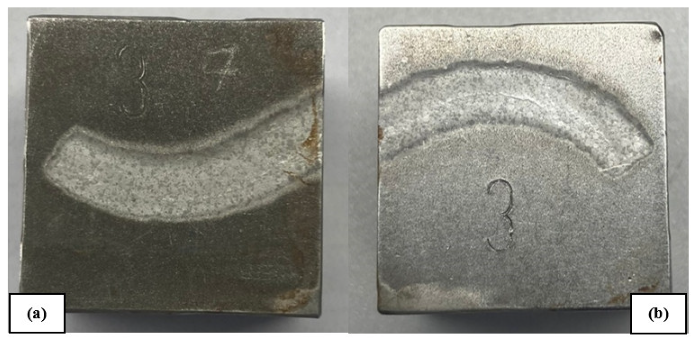
Figure 1. Photographs of the (a) W-EDMed and (b) VFed surfaces after EC grooving.
Machines 11 00823 g001
Figure 2. Schematic of the machining area.
Machines 11 00823 g002
Figure 3. Taper angle definition and groove geometry of the EC grooved surface.
Machines 11 00823 g003
Figure 4. Preparation of the specimens for the SEM analysis VFed: (a) Specimen, (b) Thick part, (c) Thin part, (d) The area of the SEM Analysis; W-EDMed (e) Specimen (f) Thick part, (g) Thin part, (h) The area of the SEM Analysis.
Machines 11 00823 g004
Figure 5. Variation of MRR with voltage for (a) VFed and (b) W-EDMed surfaces.
Machines 11 00823 g005
Figure 6. Variation of MRR with gap distance for (a) VFed and (b) W-EDMed surfaces.
Machines 11 00823 g006
Figure 7. Schematic of the WL effect on the EC grooving and electric circuit diagrams (created with BioRender.com).
Machines 11 00823 g007
Figure 8. SEM images of non-EC grooved specimens at low (ac) and high (bd) magnificent for W-EDMed (a,b) and VFed (c,d) specimens.
Machines 11 00823 g008
Figure 9. Effect of voltage on the surface roughness for (a) VFed and (b)W-EDMed.
Machines 11 00823 g009
Figure 10. Effect of gap distance on the surface roughness for (a) VFed and (b)W-EDMed.
Machines 11 00823 g010
Figure 11. Effect of EC grooving parameters on the groove profile geometry for VFed (ac) and W-EDMed (df) surface type.
Machines 11 00823 g011
Figure 12. Backscattered SEM images of cross-sections after the EC grooving for (a) W-EDMed and (b) VFed surfaces.
Machines 11 00823 g012
Figure 13. SEM images of Vfed + EC grooved grooves at 20 V—1.5 mm (a) and 15 V—1.5 mm (b) gap distances and (c) schematic of EC grooving.
Machines 11 00823 g013
Figure 14. Variation of taper angle with surface type for different (a) voltages and (b) gap distances.
Machines 11 00823 g014
Table 1. Chemical composition and mechanical properties of Stellite 21.
Atomic Weight (%)
ElementCoCrNiFeMo
Stellite 21Balance25–272.2–2.513–1.55.5–6.0
Mechanical Properties
Hardness (HRB)Tensile Strength Modulus of ElasticityThermal Conductivity
103724 MPa248 GPa14.7 W/mK
Table 2. Properties of PLA and apparatus.
PLAApparatus
Density 1.25 (g/cm3)Size30 × 30 × 60 mm3
Tensile strength45 MPaMachining area46 × 3.5 mm2
PatternHoneycombPipe diameter8 mm
Infill rate%100Electrolyte output1 mm
Table 3. Experimental Conditions.
EC Grooving Parameter
Voltage (V)Gap (mm)SurfaceConductivity (mS/cm)Machining Time (s)Flow Rate (lt/min)
10–15–201–1.25–1.5W-EDMed
VFed
105654
Disclaimer/Publisher’s Note: The statements, opinions and data contained in all publications are solely those of the individual author(s) and contributor(s) and not of MDPI and/or the editor(s). MDPI and/or the editor(s) disclaim responsibility for any injury to people or property resulting from any ideas, methods, instructions or products referred to in the content.