1. Introduction
Following LIGO’s successful detection of gravitational waves (GWs) in the ground [
1,
2], GW detection has gradually become a globally hot research topic. However, ground-based detectors [
3,
4,
5] are insensitive to GWs below 1 Hz due to terrestrial gravity gradient noise. To detect a broader range of astrophysical GW sources in the low-frequency band (0.1 mHz–1 Hz), several space-based missions—such as LISA [
6], Taiji [
7], and TianQin [
8]—have been proposed. These missions all employ laser interferometers with ultra-long baselines (~millions of kilometers) to measure picometer-level distance variations induced by GWs between free-floating test masses. Since these distance variations proportionally shift the phase of the interferometric signal, relative displacement measurements are converted into phase measurements.
The Phase Measurement System (PMS), also known as the phasemeter, is one of the key elements of an inter-satellite laser interferometer, which is used to measure the phase change in the sinusoidal beat note synchronously and continuously. According to the noise allocation budgets of space-based GW detection missions [
9,
10], the PMS must limit its noise contribution to
within the frequency range of 3 mHz to 1 Hz, which translates to a phase noise requirement of
. Additionally, the PMS has to handle three lower-level beat notes (one carrier-carrier and two sideband-sideband) with different amplitudes and a pilot tone set to 5 MHz in a single input signal simultaneously. These beat notes exhibit Doppler-induced frequency variations of up to 25 MHz [
11].
Such stringent requirements render conventional phase measurement techniques—including in-phase/quadrature (I/Q) demodulation [
12], zero-crossing detection [
13], and cross-correlation analysis [
14]—inadequate. To address this, Wand et al. [
15] developed a new type of PMS in 2006, utilizing a digital phase-locked loop (DPLL) to directly track the frequency change in input signal. Digital three-signal test validated the noise floor of DPLL better than
within the 1 mHz–1 Hz band. However, analog split test revealed that the performance of the PMS was constrained by ADC jitter noise, which would cause significant performance degradation at high input frequency. Subsequently, Gerberding et al. [
16] developed a precise ADPLL model and implemented a multi-channel PMS on a Field-Programmable Gate Array (FPGA). As a digital circuit, ADPLL is less susceptible to power supply noise, substrate noise, and parasitic effects, which typically affect the performance of analog PLLs. Additionally, the digital architecture offers high scalability on FPGA. This architecture meets the multi-channel, high-speed, and high-precision requirements of the PMS for space-based GW detection. In order to implement the correction of ADC jitter in data post-processing, a redesigned analog front-end (AFE) integrated active pilot tone injection was developed [
17,
18,
19]. This enabled the performance of PMS to meet the mission requirement over the input frequency range of 5–25 MHz. In parallel, the Taiji and TianQin teams engineered dedicated PMS units [
20,
21] leveraging LISA’s pioneering work. The ADPLL-based PMS has now passed performance verification under LISA conditions [
22] and have been successfully used in the Laser Ranging Interferometer (LRI) on GRACE Follow-On [
23].
In summary, ADPLL has evolved into a robust phase measurement technique and is now the standard solution for phase readout in inter-satellite laser interferometers. Its performance is essential for future spaceborne interferometry missions. However, existing studies have predominantly focused on analog front-end impacts on PMS performance, overlooking fundamental constraints of the ADPLL technique itself. To address this gap, we conduct a systematic analysis of parameter impacts on ADPLL stability and performance using Gerberding’s linear model. We further propose a detailed loop parameter design workflow and a comprehensive noise model, both of which can serve as quantitative guidelines for optimizing ADPLL designs to meet specified bandwidth and precision requirements. A symmetrical balance is inherent in the loop filter design, trading off tracking agility (wide bandwidth) against noise suppression (narrow bandwidth). As detailed in
Section 4, identifying this optimum is essential for achieving a high-fidelity PMS. To validate our analysis, a modified digital split test is proposed to evaluate the ADPLL’s performance across various parameter configurations. Crucially, all tests are implemented on an FPGA platform.
2. The Principle of PMS Based on ADPLL
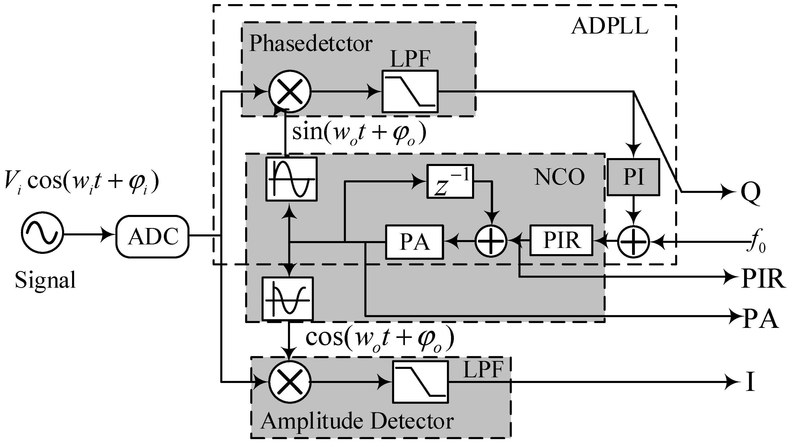
The mainstream architecture of the PMS is shown in
Figure 1, which can be regarded as a fusion product of IQ quadrature demodulation and ADPLL. Specifically, the ADPLL constitutes the core quadrature branch with frequency and phase tracking capabilities. Another optional in-phase branch can be used to measure the amplitude of the input signal.
The ADPLL comprises a phase detector, a proportional-integral (PI) controller, and a numerically controlled oscillator (NCO). Its principle is to generate a digital sine wave within the NCO and synchronize this signal with the input via a digital servo loop. The input signal is first quantized by an ADC, then mixed separately with two quadrature signals from the NCO, also known as local oscillator (LO) signals. After low-pass filtering (LPF) removes the sum-frequency component, the in-phase (
I) and quadrature (
Q) branch outputs are derived as follows:
where
. For small in-loop phase changes (
), the signal
can be linearized as a proportional term of the phase itself (
), while the signal I scales with the input signal amplitude (
). Consequently,
serves as the phase error signal. Then, through further filtering by the PI controller, this error signal is converted into a feedback signal to be fed into the actuator NCO. The NCO dynamically adjusts the frequency and phase of its output sine wave to drive the DC component of
toward zero, thereby achieving phase lock.
Such an ADPLL enables robust tracking of input signal frequency variations. By configuring the loop bandwidth and initializing distinct frequency control words in the NCO, multiple ADPLL channels can simultaneously and independently track heterodyne beat notes of differing frequencies within a composite input signal.
When the loop maintains stable phase lock, the NCO-generated sine wave matches the input signal frequency while maintaining a 90° phase offset. Under this condition, the input signal’s phase information is completely transferred from the signal to the NCO. The Phase Increment Register (PIR) and Phase Accumulator (PA), respectively, store instantaneous frequency and phase information of the LO signal. Consequently, input signal phase reconstruction is achieved by reading either the PIR or PA. For diagnostic purposes, the signals and are also read out. The arctangent of their ratio () provides auxiliary phase correction, ensuring high-fidelity phase reconstruction under dynamic or low signal-to-noise conditions.
The principle of symmetry plays a crucial role in the performance of quadrature phase detection systems like the one employed here. The amplitude and phase symmetry between the in-phase and quadrature channels is critical for minimizing DC offsets and even-order harmonic distortions, which directly impacts the linearity and accuracy of phase detection. Maintaining this symmetry in the digital domain is a key advantage of the ADPLL architecture, contributing to its superior noise resilience.
As the core component of the PMS, the ADPLL’s tracking precision fundamentally determines overall system performance. This precision is governed by two key parameters: loop stability and input noise level, both quantifiable through transfer functions derived from the system block diagram.
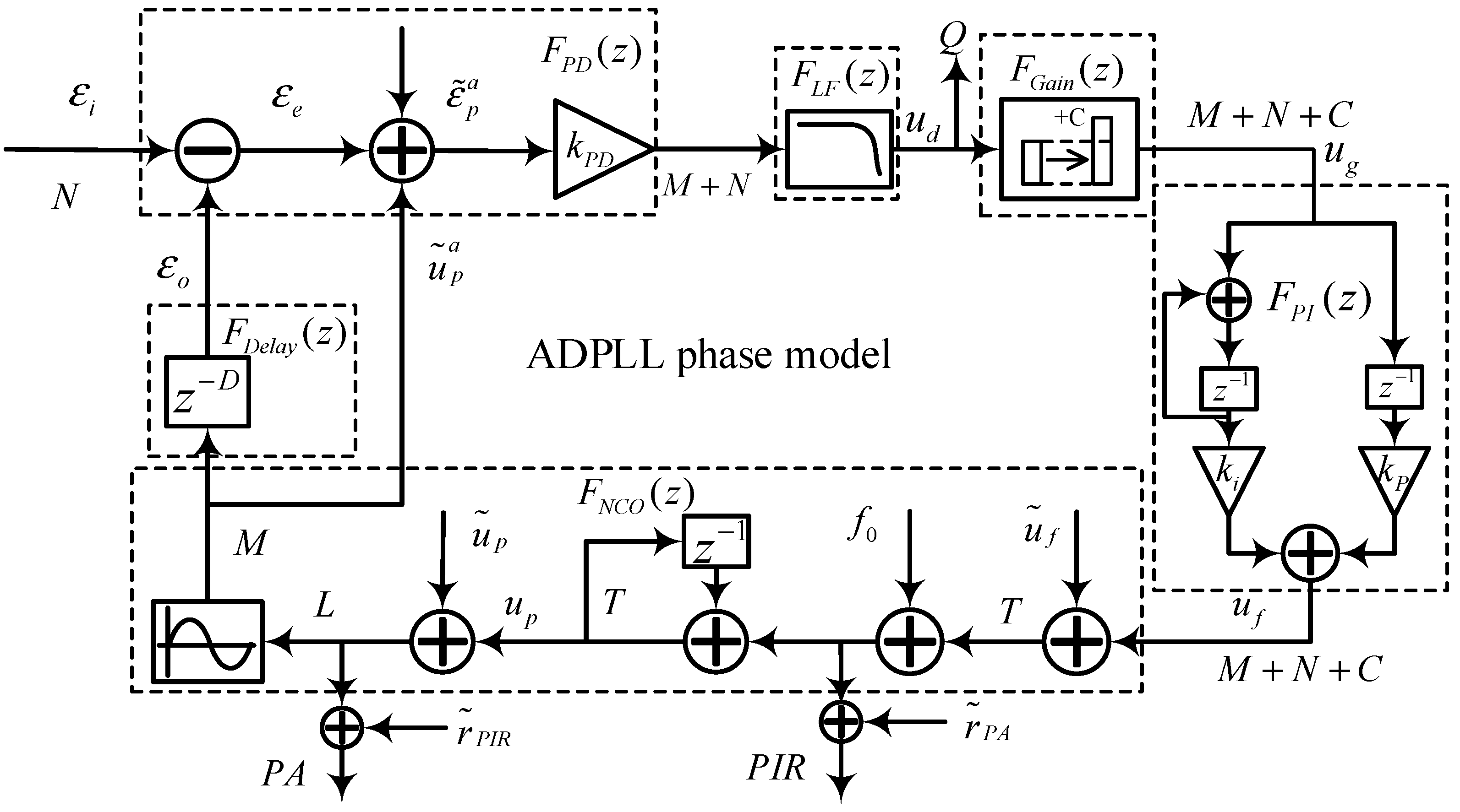
Figure 2 presents a modified ADPLL linear model adapted from Gerberding’s framework [
16], where phase serves as the sensed and actuated quantity. The model incorporates three critical noise sources:
- (1)
PA readout noise
;
- (2)
PIR readout noise ;
- (3)
Phase noise caused by amplitude quantization.
Based on the linear model shown in
Figure 2, the z-domain open-loop transfer function
of the ADPLL can be derived from the cascade of its constituent blocks [
16]:
where
denotes the phase detector transfer function with
A (0 ≤
A ≤ 1) being the normalized gain contributed by the input signal. This gain is defined as the ratio of the peak-to-peak value of the input signal to the maximum peak-to-peak voltage range of the ADC.
and
are the transfer function of the low pass filter (LFP) and NCO, respectively. The gain control module transfer function
achieves a loop gain of
through M-bit sign-bit extension of the signal
. The PI controller transfer function
incorporates proportional and integral gain coefficients
and
. Finally,
represents the delay module transfer function, where
D denotes the total loop processing latency in clock cycles.
Based on the open-loop transfer function
, the system transfer function
and the error transfer function
can be derived. These characterize the loop’s responses to distinct input noise sources as follows:
3. Loop Parameter Design Workflow
Bandwidth
and phase margin
are two fundamental indices in control system design. Bandwidth characterizes the system’s dynamic response speed, defined as the frequency range where the closed-loop transfer function magnitude remains within −3 dB of its DC value. Phase margin quantifies stability robustness, numerically equal to the difference between the phase at the unity gain angular frequency
of the open-loop transfer function and
. To ensure stable ADPLL operation within a specified bandwidth, precise analytical relationships must be established between the loop parameters (
,
,
D,
C,
A) and both
and
. We first convert the z-domain transfer function
to its s-domain equivalent
via backward Euler transformation to facilitate subsequent frequency-domain stability analysis. According to the mapping relationship between the z-domain and s-domain,
is given by:
where
is the sampling frequency. To make Equation (4) more concise, the following definitions are made:
Then
can be rewritten as:
Generally, the normalized gain A and sampling frequency are both pre-determined and cannot be adjusted in the program. Therefore, we will treat them as constants in the following analysis.
Since the magnitude-frequency responses of the transfer functions for both the delay term and the low-pass filter approximate unity within the bandwidth, these terms can be temporarily neglected. Following this simplification,
reduces to the open-loop transfer function of a standard second-order type-II PLL. The loop dynamics are fully characterized by two parameters: the natural angular frequency
and the dimensionless damping factor
. The system transfer function
is thus expressed as:
with
and
An explicit analytical relationship exists between phase margin
and damping factor
, exhibiting a strong positive correlation. The preferred damping factor value is
, corresponding to
. In practical implementations, the damping factor
is typically preset to a value greater than 1 to compensate for significant phase lag introduced by the LPF and delay term. This ensures the actual loop has a phase margin of
. At such a large damping value, the closed-loop bandwidth
, unity-gain angular frequency
, and natural angular frequency
satisfy the following approximate relationship:
By combining Equations (7), (8) and (10), the recommended values of
and
for a target bandwidth and damping factor are given by:
It should be noted that the computed and values should be rounded to the nearest integer power of two. This facilitates hardware-efficient implementation where multiplication operations are replaced by bit-shift operations.
To accurately estimate the phase margin
of the loop, the phase lag introduced by the low-pass filter (LPF) and the delay term must be incorporated. Per the formal definition of phase margin, this yields:
where
denote the phase of the LPF at the unity-gain angular frequency
Per Equation (10),
can be approximated by the target bandwidth
. Then substituting the computed
and
values into the above equation, the first term can be determined. The primary function of the LPF is to attenuate second harmonics in the error signal. While higher-order LPFs improve harmonic suppression, they simultaneously increase logic resource utilization and introduce greater phase lag. After evaluating the trade-offs between these factors, an infinite impulse response (IIR) filter architecture is more recommended. The design and implementation of this filter depends on the exact loop design and should be adapted accordingly.
The phase lag attributed to the delay term exhibits linear dependence on both the total delay D (clock cycles) and the target bandwidth . This phase lag becomes critically significant in high-bandwidth designs. The value of D can directly be computed from the number of registers used in the loop logic. For the space-based GW detection missions, PMS typically operates at a rate of 80 MHz, which is sufficient to enable phase measurement of a heterodyne signal with a maximum frequency of approximately 25 MHz. At such a high operation rate, the LPF, multiplier, and lookup table each introduce a delay of one clock cycle, leading to D = 3.
To summarize, the parameter design and optimization procedure proceeds as follows:
- (1)
Determine the algorithm operating rate and input signal gain A;
- (2)
Calculate preliminary controller parameters with preset for stability margin and target bandwidth by Equations (11);
- (3)
Design an LPF and determine its phase lag at the angular frequency of target bandwidth ;
- (4)
Determine the total number of delay clocks D;
- (5)
Determine the actual phase margin based on the results of Steps 2–4;
- (6)
Fine-tune the LPF to achieve the desired phase margin.
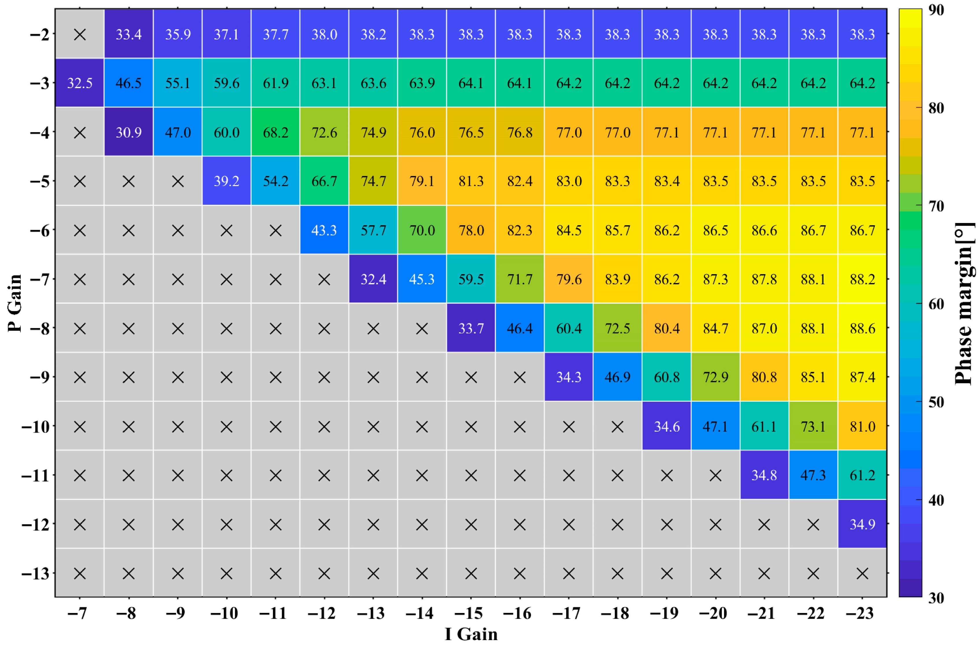
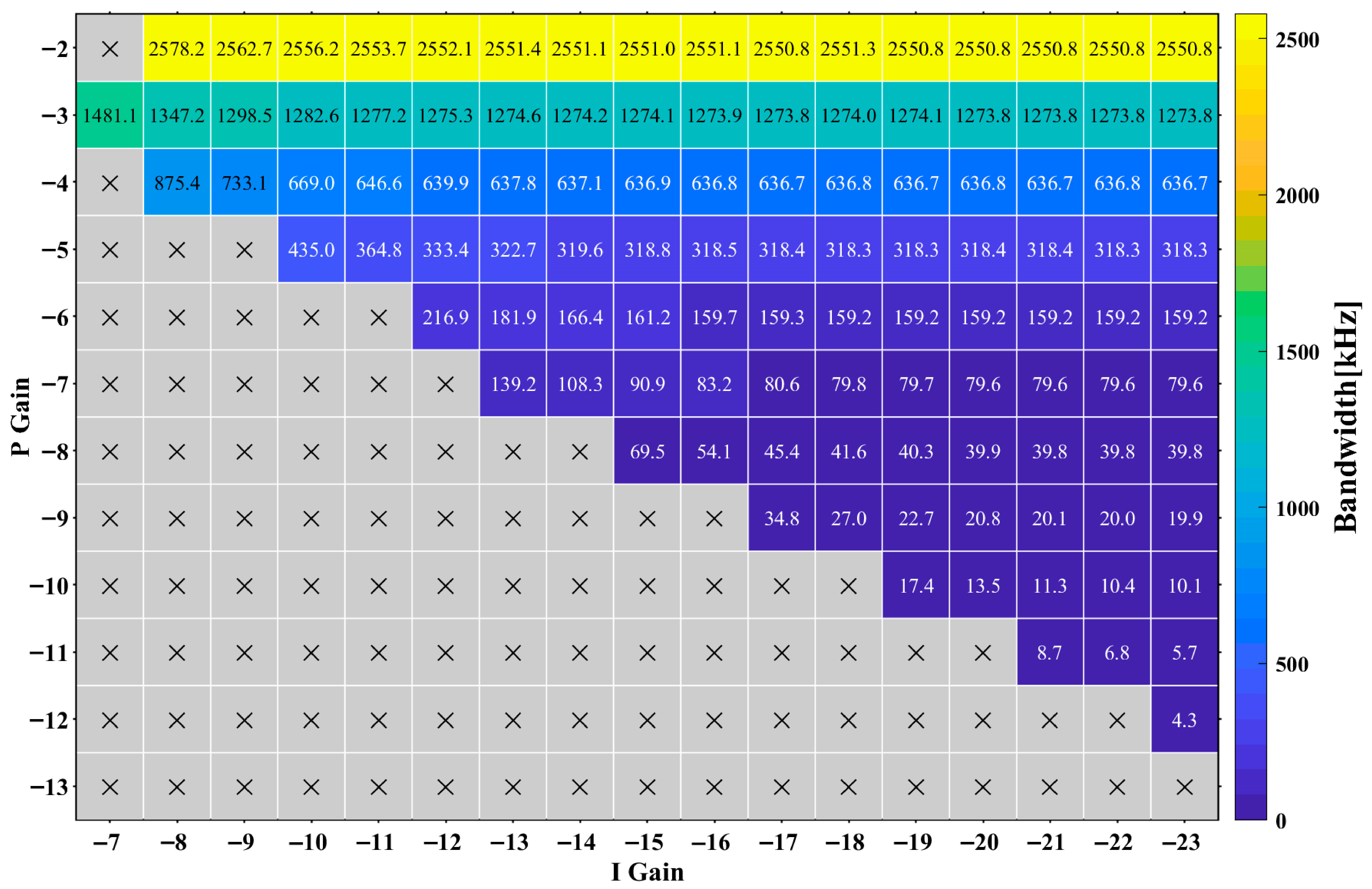
To facilitate PMS design replication, we computed the ADPLL bandwidth and phase margin across discrete proportional-integral gain pairs (
,
) with results visualized in
Figure 3 (bandwidth vs. gains) and
Figure 4 (phase margin vs. gains). These simulations employed the following nominal conditions:
,
D = 3, and
A = 0.8.
4. Noise in an ADPLL
This section details diverse noise sources in an ADPLL and their induced phase noise contributions. Crucially, all subsequent analysis assumes small phase tracking errors where linear control theory applies. Specifically, when the noise level surpasses a threshold, the loop will enter a nonlinear operating regime. In this regime, the established transfer function becomes inapplicable, rendering the theoretical model inaccurate.
4.1. Noise in Input Signal
4.1.1. Input Phase Noise
Accounting for inherent signal imperfections, the analog input signal
with combined additive noise
and phase noise
is expressed as:
where
is the amplitude of the signal,
is the frequency of the signal. The PLL is unable to distinguish between the input phase noise
and the nominal phase
, so both are tracked collectively as input phase
. The untracked portion of
manifests as a residual phase error
, whose ASD is given by:
where
represents the s-domain error transfer function equivalent to
. Given specified input phase noise ASD and target residual phase error, the above equation can be employed to determine the open-loop gain required for the loop to suppress input phase noise, which is provided by
.
Under the second-generation Time-Delay Interferometry (TDI 2.0) framework, LISA’s laser frequency noise requirement relaxes to the following amplitude spectral density (ASD) specification [
24]:
where
is the noise shape function (NSF) (
). Assuming identical laser frequency noise levels in master and slave satellites, the amplitude spectral density (ASD) of input phase noise during beat note acquisition is:
To incorporate design margin, the residual phase error amplitude spectral density is set to
. The minimum required open-loop gain magnitude must therefore satisfy:
4.1.2. Input Additive Noise
Additive noise, while not a direct phase error, degrades PLL tracking precision by inducing jitter in the phase detector output. For an approximately white noise source around a strong carrier signal, this effect is modeled as equivalent phase noise
with the following formula [
25]:
where
is the value of the additive noise ASD at input frequency
. Additive noise introduced during optoelectronic conversion—primarily comprising shot noise, electronic noise, and relative intensity noise (RIN)—exhibits approximately white spectral characteristics within a narrow band around the heterodyne frequency. For the additive noise term
in Equation (13), the ASD of resulting equivalent phase noise
is:
After propagating through the loop, the additive phase noise
leads to an additional phase error
in the error signal:
where
represents the s-domain system transfer function equivalent to
. This function exhibits low-pass characteristics. Consequently, low-frequency components of the additive phase noise
below loop bandwidth propagate essentially unattenuated.
Owing to their ultra-long arm lengths, space-based interferometers operate at critically low received optical power levels: 700 pW for LISA, 1.2 nW for Taiji, and 78 nW for Tianqin. These mission-specific values are derived from fundamental parameters: laser output power, interferometer arm length, telescope aperture diameter, and overall optical efficiency in the receive path. At such received power levels, shot noise dominates the additive noise floor. The total variance of the phase error
is therefore governed by two primary sources:
This expression enables evaluation of loop linearity. By evaluating the total phase error variance across varying loop bandwidths , the ADPLL can be optimized to operate within the linear regime. This minimizes nonlinear distortion and cycle slip probability.
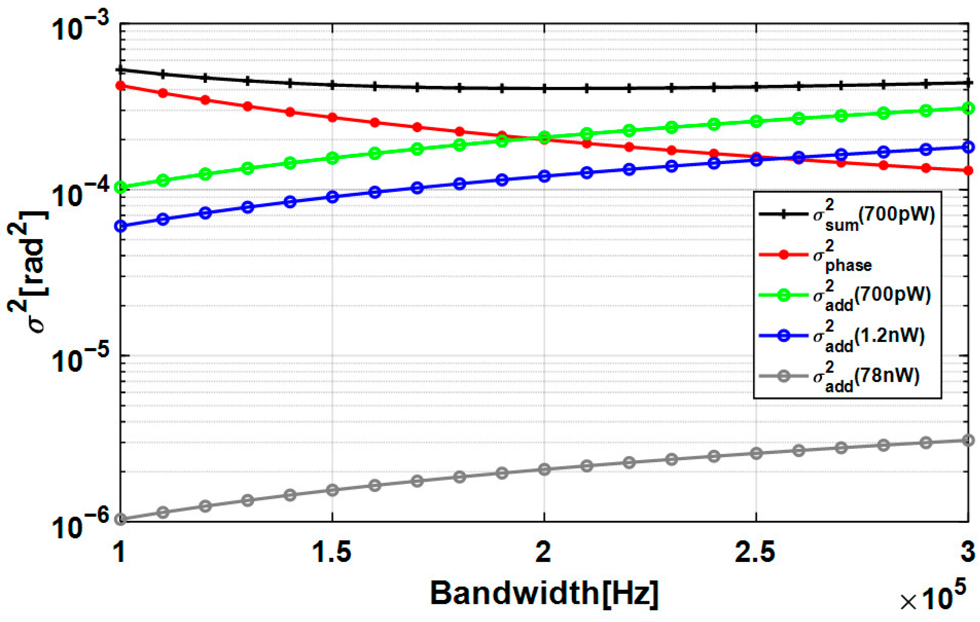
Figure 5 shows the calculated total phase error variance under diverse bandwidth configurations for LISA’s received optical power of 700 pW. The high-frequency component of the laser frequency noise ASD used here is taken from the experimental results in reference [
17]. As anticipated by Equations (14) and (20), the variance of additive-noise-induced phase noise increases as the PLL bandwidth increases (red line), whereas the variance of input-phase-noise-induced phase noise decreases as the bandwidth increases (green line). For comparative analysis, the phase error variance caused by shot noise is also calculated and presented for two additional received optical power levels: 1.2 nW (blue line) and 78 nW (gray line). Under the current input noise conditions, the optimal bandwidths of the PMS for the LISA and Taiji missions are determined to be 200 kHz and 250 kHz, respectively. For the TianQin mission, the reduced shot noise enables its PMS to employ the maximum feasible bandwidth, thereby minimizing the residual phase error originating from input phase noise.
4.2. Noise in NCO
Similarly to the input signal, the LO signal generated by the NCO exhibits phase noise and additive noise. As shown in
Figure 2, the NCO introduces three primary noise components: frequency truncation noise
, phase truncation noise
, and amplitude quantization noise
. These noises correspond to the truncation of PIR, PA, and the amplitude quantization of LO signal, respectively. For the truncation of a continuous signal to a digital number with
N bits at a sampling rate
can be modeled as an addition of uniformly distributed white noise
with ASD:
The same formula is also applied here for the truncation of digital signals. However, such truncation will also introduce numerous spurious signals into the LO signal, particularly phase truncation. This affects the loop in two ways:
To suppress these spurs, a random sequence—termed dither—must be added to the digital signal prior to truncation [
26]. For truncation from
T bits to
L bits, it is recommended to employ a triangular distribution dither with a bit length of
T −
L + 1. The dithered truncation also introduced effective white noise. This will lead to a higher noise floor with ASD, as follows:
The frequency resolution
of the NCO with a
T-bit PIR is
. For dithered truncation from (
M +
N +
C) bits to
T bits, the ASD of the frequency truncation noise
is:
According to the relationship between frequency and phase, the phase noise
corresponding to the frequency truncation noise
is given by:
Similarly, the ASD of the phase truncation noise
generated by the truncation from (
T) bits to
L bits in the PA can be express as:
The amplitude quantization noise
, distinct from the aforementioned phase and frequency truncation noises, constitutes an additive noise component. Based on Equation (18), the ASD of the phase noise
induced by
M-bit amplitude quantization is given by:
Combining the PLL’s distinct transfer responses to additive noise and phase noise derived in
Section 4.1, the ASD of total phase error
in loop introduced by the NCO is:
It can be seen that the ADPLL allows aggressive quantization bit reduction in both the PIR and PA, as their truncation noises are suppressed by the error transfer function . For example, a 12-bit PIR truncation maintains a performance of 1 µcycle between 0.1 mHz and 1 Hz in an 80 MHz system. Consequently, these two truncation points are highly recommended for bit reduction. However, the bit lengths of PIR and PA also directly impact the readout precision of the PMS, a relationship that will be analyzed in the next section.
4.3. Readout Noise
As noted in
Section 2, phase reconstruction depends on the readout of the PA or PIR. Since both PA and PIR are represented with a finite number of bits, their quantization levels impose a fundamental noise limit on the readout results, termed readout noise. Based on the truncation noise (without dither) analysis in the previous subsection, the ASDs of PA readout noise
and PIR readout noise
can be expressed as:
and
where
L and
T denote the readout bit widths of the PA and PIR, respectively. Note that both PA and PIR readout noise directly couples into the final phase measurement results. Consequently, to achieve the target phase readout precision of
, the bit length of the PA must be no less than 7 and that of the PIR must be no less than 38.
Typically, the signal of interest must be downsampled to the target rate in the FPGA to facilitate subsequent storage and computation. A high-order cascaded integrator-comb (CIC) filter is commonly employed as the anti-aliasing filter prior to decimation [
27]. However, full-precision CIC implementation significantly increases output bit width, where most bits represent insignificant LSBs. Truncation at the readout interface is therefore essential. The required readout bit lengths for PIR and PA after downsampling can be determined using Equations (29) and (30).
In space-based GW detection missions, offset-frequency weak-light phase locking combined with a specific frequency plan enables dynamic adjustment of the slave satellite’s laser frequency [
28]. This ensures the beat note remains within a reasonable range, preventing PIR overflow while allowing individual PIR readout after downsampling. In the time domain, the PA represents the integral of the PIR. Its value rapidly overflows, generating a sawtooth waveform that induces aliasing artifacts during downsampling. When multiple ADPLL channels track identical-frequency signals, differencing their PA values cancels the common ramping component. The differential output directly measures the inter-channel phase difference. Consequently, PA values must be differenced immediately before readout.
5. Digital Measurements
To validate the loop parameter design workflow in
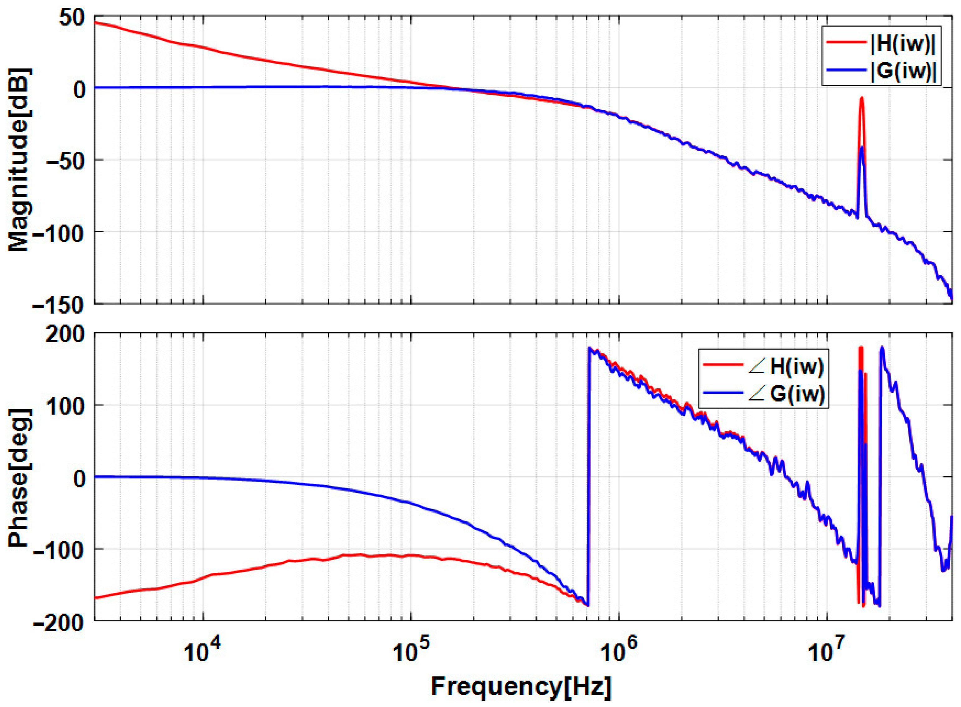
Section 3, we implemented an FPGA-based ADPLL targeting 200 kHz bandwidth using this workflow. To ensure the actual loop has sufficient phase margin, the damping factor was set to 2. The proportional and integral gains were then calculated using Equation (11). The parameter configurations are detailed in
Table 1. By injecting broadband white noise perturbations into the error signal, the frequency response of both the system and the open-loop transfer functions for this loop were estimated. The results are presented in the Bode plot in
Figure 6. The peak at 14 MHz in the Bode plot is caused by the sum-frequency component in the phase detector output which is neglected in Equation (1). The results indicate a loop bandwidth of approximately 180 kHz and a phase margin of approximately 60°. The 20 kHz bandwidth discrepancy (180 kHz vs. 200 kHz) stems from controller parameter truncation but remains negligible in practice. A second-order IIR filter suppresses the second harmonic, with its phase lag compensated by the deliberately large damping factor
. Nevertheless, the achieved phase margin of 60° ensures robust ADPLL stability.
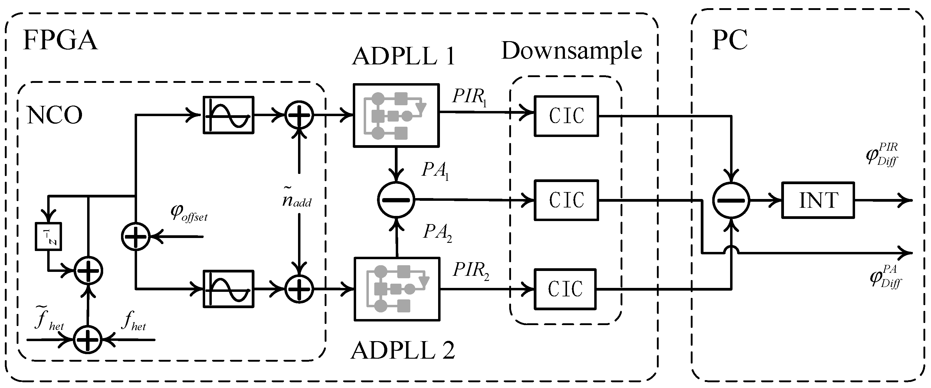
To characterize the noise influence, we performed FPGA-based measurements of the ADPLL performance. We implemented a scheme based on a modified digital splitting measurement (the setup is shown in
Figure 7). A digital test signal with controlled noise generated by the NCO is split into two identical ADPLLs for independent tracking. The differential phase between both channels’ outputs isolates the loop noise, as input signal noise constitutes a common-mode component rejected by differencing. Each measurement reconstructs the differential phase through both PIR and PA readouts, yielding results referred to as differential PIR phase
and differential PA phase
, respectively. An adjustable phase offset is introduced into one signal path to prevent a null measurement which is insensitive to nonlinear noise. All experiments in this study were implemented on a Terasic TR-530 development board equipped with a Stratix IV GX EP4SGX530C2 FPGA. Since the Terasic TR-530 development board lacks a built-in UART interface, an external USB-to-TTL module was used to facilitate data transmission between the FPGA and the computer.
As established earlier, the readout noise
and
, along with the phase noise
, cannot be suppressed by the loop and thus dominate the actual measurement results. This paper therefore exclusively verifies these three noise models. We varied the quantization bit lengths of the PA, PIR, and NCO amplitude independently, measuring the ASD of the corresponding differential phase using the setup shown in
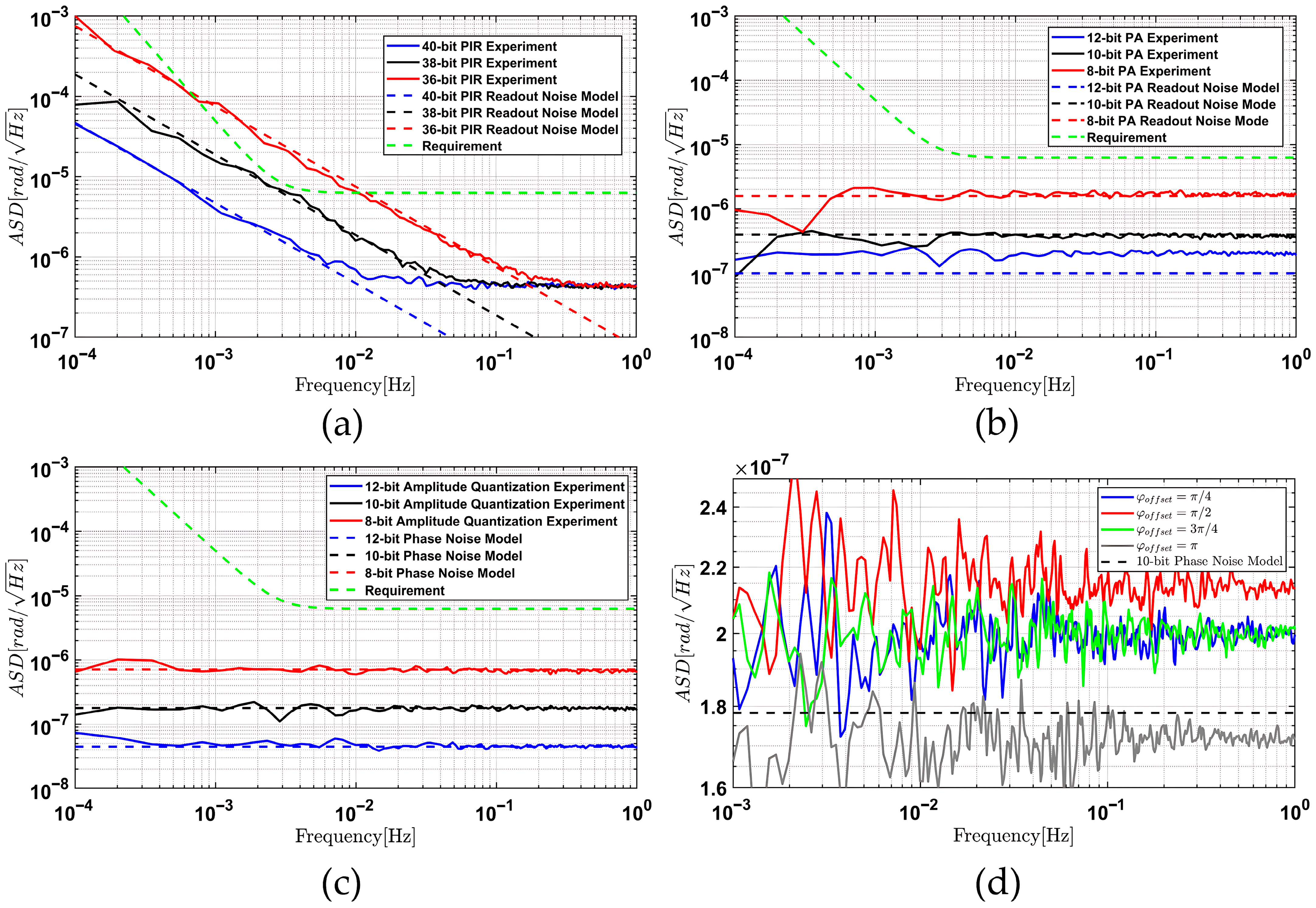
Figure 8. For each configuration, the PMS Verilog code was recompiled. Measurements lasted ≥ 3 h to ensure the statistical significance of ASD values down to 1 mHz. Crucially, since bit length modifications alter loop dynamics, controller parameters were fine-tuned to maintain consistent closed-loop bandwidth across all tests.
The experimental results are presented in
Figure 8. For comparison, the sensitivity requirement curve of the PMS and the theoretical noise curve are also presented.
Figure 8a shows the measured ASD of the differential PIR phase for PIR bit lengths of 40, 38, and 36 bits. As predicted, PIR quantization imposes a 1/f noise floor limiting low-frequency PMS sensitivity, with measured noise fully aligning with the theoretical PIR readout noise model.
Figure 8b displays the ASD of the differential PA phase for PA bit lengths of 12, 10, and 8 bits. Here, PA quantization sets a white noise limit on PMS sensitivity. Crucially, the 12-bit PA configuration exhibits higher noise than predicted by PA readout noise model. A comparison between Equations (27) and (29) reveals that, for an identical bit length, the ASD of PA readout noise
is 2.2 times that of the phase noise
. However, in this experiment, the amplitude quantization bit length utilized was only 10—2 bits fewer than the 12-bit PA quantization. This leads to the phase noise
surpassing the PA readout noise
. Consequently, we ascribe the higher-than-expected noise to the phase noise
under 10-bit amplitude quantization.
To prevent readout noise contamination during verification of the model of additive phase noise
, the PA bit length was set to 2 bits more than the amplitude quantization bit length in subsequent experiments. Under this configuration, the measured ASD of the differential PA phase for amplitude quantization bit lengths of 12, 10, and 8 bits shows excellent agreement with theoretical predictions, as validated in
Figure 8c. Additionally, we characterized loop-inherent nonlinear noise by deliberately varying the phase offset
between the input signals of the dual ADPLL channels. As shown in
Figure 8d, nonlinear noise contributes negligibly to PMS performance degradation. Its amplitude scales proportionally to
, consistent with theoretical predictions for second-harmonic-type nonlinearities. It can be further suppressed by a higher-order low-pass filter.
