Abstract
To address the common issues of high small object miss rates, frequent false positives, and poor real-time performance in PCB defect detection, this paper proposes a multi-scale fusion algorithm based on the YOLOv12 framework. This algorithm integrates the Global Attention Mechanism (GAM) into the redesigned A2C2f module to enhance feature response strength of complex objects in symmetric regions through global context modeling, replacing conventional convolutions with hybrid weighted downsampling (HWD) modules that preserve copper foil textures in PCB images via hierarchical weight allocation. A bidirectional feature pyramid network (BiFPN) is constructed to reduce bounding box regression errors for micro-defects by fusing shallow localization and deep semantic features, employing a parallel perception attention (PPA) detection head combining dense anchor distribution and context-aware mechanisms to accurately identify tiny defects in high-density areas, and optimizing bounding box regression using a normalized Wasserstein distance (NWD) loss function to enhance overall detection accuracy. The experimental results on the public PCB dataset with symmetrically transformed samples demonstrate 85.3% recall rate and 90.4% mAP@50, with AP values for subtle defects like short circuit and spurious copper reaching 96.2% and 90.8%, respectively. Compared to the YOLOv12n, it shows an 8.7% enhancement in recall, a 5.8% increase in mAP@50, and gains of 16.7% and 11.5% in AP for the short circuit and spurious copper categories. Moreover, with an FPS of 72.8, it outperforms YOLOv5s, YOLOv8s, and YOLOv11n by 12.5%, 22.8%, and 5.7%, respectively, in speed. The improved algorithm meets the requirements for high-precision and real-time detection of multi-category PCB defects and provides an efficient solution for automated PCB quality inspection scenarios.
Keywords:
PCB defect detection; YOLOv12; GAM module; HWD module; BiFPN; PPA detection head; NWD loss function 1. Introduction
Printed Circuit Boards (PCBs), as core components of modern electronic devices, directly impact the functional stability and service life of electronic systems through their manufacturing quality [1]. With the rapid development of electronics toward miniaturization and high-density integration [2], PCB surface defects such as mouse bites, short circuits, and spurious coppers [3] have become increasingly complex and diverse. These defects are prone to being overlooked in traditional inspection processes, leading to potential risks like circuit shorting and signal transmission anomalies. Particularly in high-reliability fields such as 5G communications and aerospace, PCB defects may trigger cascading equipment failures, resulting in significant economic losses and safety hazards [4]. This underscores the urgent need for intelligent defect detection technologies with high precision and efficiency.
Conventional PCB defect detection predominantly relies on human visual assessment [5] and computerized image analysis systems [6]. The former suffers from operator fatigue and subjective judgment bias, leading to inconsistent detection reliability, while the latter, despite enabling batch image processing, exhibits sensitivity to lighting conditions and insufficient algorithmic robustness, often causing misjudgments under complex background interference [7]. Recent advancements in deep learning offer transformative solutions for industrial quality inspection, where convolutional neural network-based object detection algorithms autonomously extract defect features from massive datasets, significantly reducing dependence on manual expertise [8].
In recent years, cutting-edge progress in deep learning-powered object detection frameworks has shown significant potential in automated industrial inspection systems. Wang et al. [9] proposed theYOLOv8-PCB-based algorithm, introducing C2f_SHSA attention for local–global feature fusion, C2f_IdentityFormer for enhanced feature sensitivity, and PIoU loss to improve adaptability across defect sizes, achieving higher accuracy and edge deployment suitability. Zhou et al. [10] developed the MSD-YOLOv5 algorithm, combining MobileNet-v3 and CSPDarknet53 to construct a lightweight backbone network. Enhanced with channel attention mechanisms for feature extraction and a decoupled detection head to separate localization and classification feature learning, their approach effectively reduces model complexity while improving defect detection precision. Tang et al. [11] proposed the YOLO-SUMAS algorithm, which integrates the SCSA attention mechanism, Unified-IoU loss function, and MobileNetV4 lightweight architecture. By incorporating an ASF-SDI Neck to enhance small object detection, the model optimizes both recognition accuracy and real-time performance for PCB defects, aligning with high-density integrated industrial requirements. Yuan et al. [12] proposed the LW-YOLO model, integrating bidirectional feature pyramids and partial convolution to reduce computational redundancy, along with a novel loss function for precise bounding box optimization addressing PCB defect detection challenges with enhanced accuracy and real-time performance. Ji et al. [13] proposed the MS-DETR model, which employs a multi-stage convolutional module and Slim-Scale Adaptive Fusion architecture to enhance small defect detection capabilities. By integrating high-frequency and low-frequency information to optimize feature extraction and adopting an improved loss function to boost detection accuracy, this framework enables efficient PCB defect detection for edge devices.
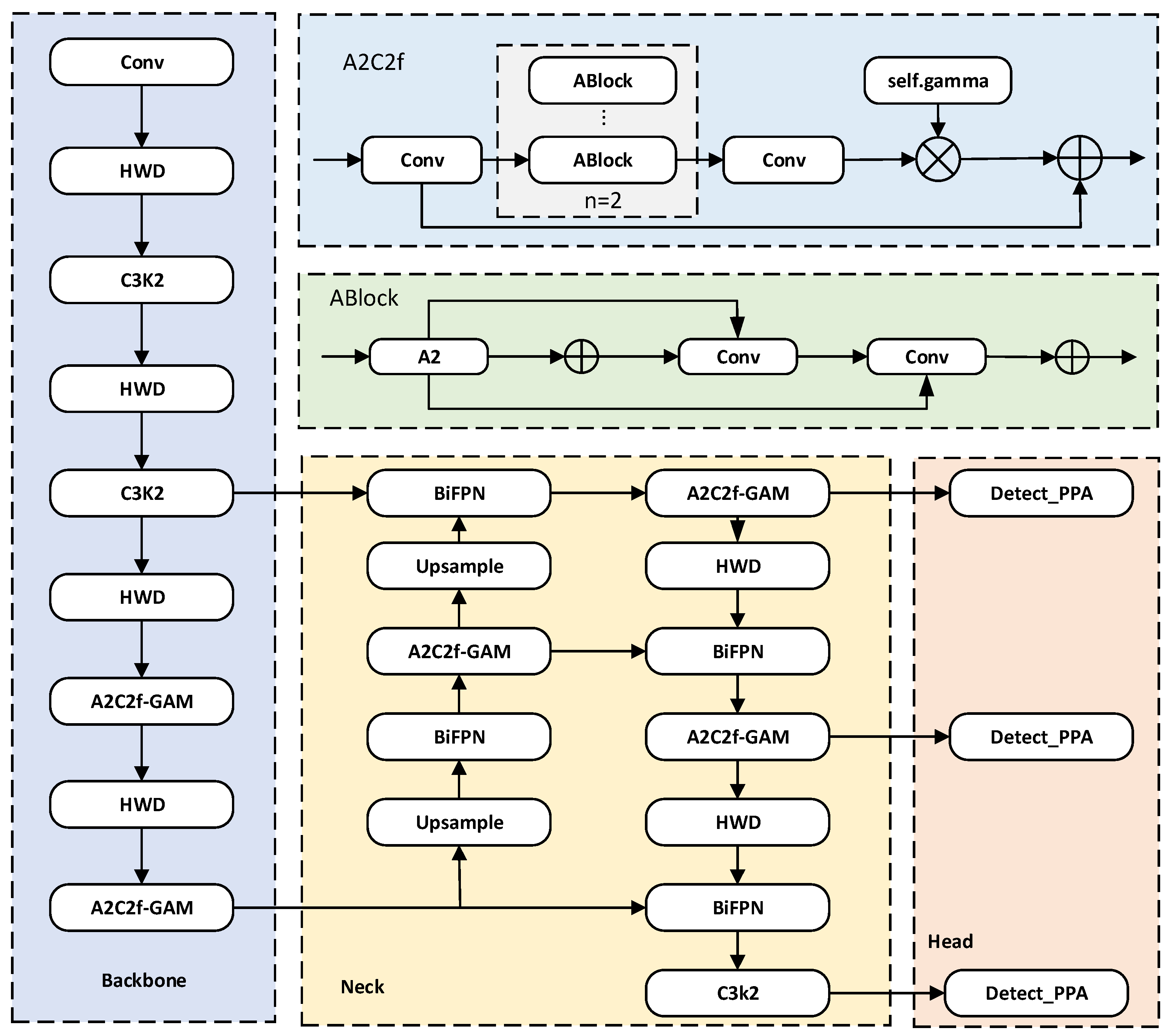
To address the challenges of easy loss of tiny object features and difficulty in capturing multi-scale defects in PCB surface defect detection [14], this paper proposes a high-accuracy algorithm for small object detection on PCB surfaces. The algorithm is an improvement over the YOLOv12, and its network structure is shown in Figure 1.
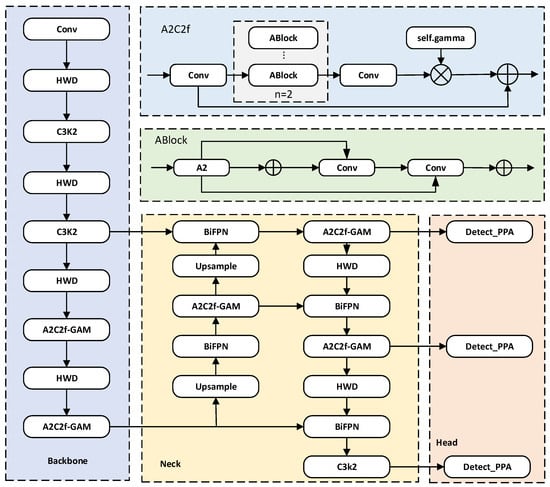
Figure 1.
The enhanced YOLOv12 network architecture with multi-module fusion.
The principal innovations of this study include the following:
- The GAM is embedded into the A2C2f module, enhancing cross-channel interactions and spatial correlations. This design significantly improve sensitivity to low-contrast defects in PCB images compared to the original A2C2f module.
- The HWD module replaces standard convolutional layers, leveraging multi-scale dilated convolutions to retain high-frequency texture features and effectively mitigate the loss of tiny defect features in PCB detection compared to standard convolutions.
- The BiFPN replaces the original contact structure in the neck network, leveraging a weighted feature fusion mechanism to optimize multi-scale feature contributions. Compared to the contact structure, the BiFPN enhances multi-scale detection capabilities for subtle defects in PCB images.
- The PPA detection head is constructed in the head network, combining local perception and global attention mechanisms to amplify responses in defect regions, reducing the missed detection rate in PCB defect inspection.
- To address the challenge of detecting small PCB defects, the NWD loss function is adopted. Compared to traditional IoU metrics, NWD employs Gaussian distribution modeling to refine localization accuracy for micro-defects.
The remainder of this paper is structured as follows: Section 2 elaborates on the proposed methodology and its technical innovations, Section 3 provides empirical validation through rigorous experiments and ablation studies, and Section 4 concludes with theoretical contributions and practical constraints for industrial deployment.
2. Methods
2.1. YOLOv12 Detection Algorithm
YOLOv12 [15], architecturally designated as the twelfth generation in the YOLO series object detection framework, demonstrates significant advantages in PCB surface defect detection with its lightweight architecture and enhanced multi-scale feature perception capabilities. By efficiently fusing local details and global contextual information, it accurately identifies microscopic defect objects. The algorithm retains the classic three-stage architecture, comprising feature extraction backbone, multi-scale fusion neck, and task-specific prediction head.
2.1.1. Backbone Network
The backbone of YOLOv12 employs a rearchitected Residual Efficient Layer Aggregation Network [16], which enhances feature extraction capabilities through stacked depthwise separable convolutions and extended residual connections. For the first time, it integrates a FlashAttention-powered area attention mechanism, dynamically focusing on critical feature regions to improve the capture of microscopic defects.
2.1.2. Neck Network
The neck innovatively integrates large kernel 7 × 7 depthwise separable convolutions and multi-scale feature interaction modules, optimized by an adaptive weight allocation strategy to enhance cross-layer feature fusion. This design preserves high-resolution details while reducing redundant computational overhead.
2.1.3. Head Network
The detection head adopts a lightweight bidirectional prediction structure, integrating a dynamic computational allocation algorithm to balance detection accuracy and inference speed. Additionally, it employs a region attention-guided dense anchor optimization strategy [17], significantly improving localization precision for complex PCB defects.
2.2. The Proposed Method
2.2.1. GAM Attention Mechanism
GAM [18] integrates channel-wise and spatial attention submodules to amplify cross-dimensional interactions, enhancing model sensitivity to low-contrast defects. Its core architecture employs parallel channel and spatial attention branches, followed by element-wise fusion for global feature calibration.
The channel attention branch adaptively learns importance weights for each feature channel to enhance responses to critical features. The channel attention module employs an MLP with an encoder–decoder-inspired dual fully connected layer architecture to generate globally adaptive channel-wise weights through feature dimensionality reduction and subsequent restoration, where the first dimensionality reduction layer leverages the ReLU activation function and contains hidden units equal to the input channel count (specifically 256 from the cv1 layer of the A2C2f module) divided by a compression ratio of 16, followed by the second restoration layer that adopts the sigmoid activation function to recover the original channel count. As shown in Figure 2, the input feature map undergoes spatial compression via GAP to generate channel-wise statistics . These statistics are then processed by two FC layers to compute channel weights , with the mathematical formulation detailed in Equations (1) and (2).
where and are learnable parameters, denotes the reduction ratio, denotes the ReLU activation function for sparse gradient propagation, and represents the sigmoid function, contrasting through smooth probability mapping.
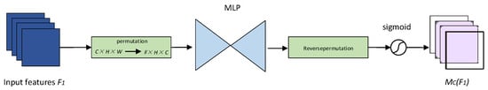
Figure 2.
The structure of channel attention module.
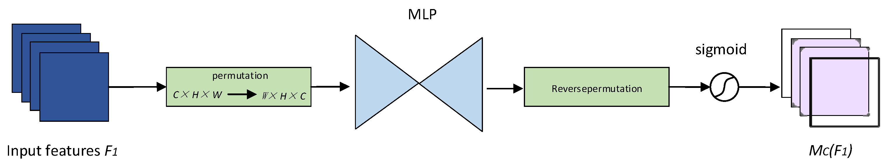
The spatial attention branch generates a spatial weight map by combining maximum and average pooling operations with dilated convolution, emphasizing salient spatial regions. As shown in Figure 3, the channel-enhanced feature map is input to the spatial transformation layer. A dual path pooling strategy first produces a two-channel feature map , which is then processed through dilated convolution and channel compression/expansion operations to generate the final spatial weight map . The mathematical formulations are detailed in Equations (3)–(5).
where is a 7 × 7 convolutional kernel: the first convolution compresses the channel dimensions, and the second convolution restores them to a single channel.
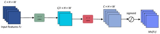
Figure 3.
The structure of spatial attention module.
The feature maps first undergo channel attention to recalibrate semantic importance across channels, then pass through spatial attention to refine positional features, achieving dual cross-dimensional calibration. The final output preserves the original features through residual connections, with the overall architecture illustrated in Figure 4. The computational steps are detailed in Equations (6)–(8).
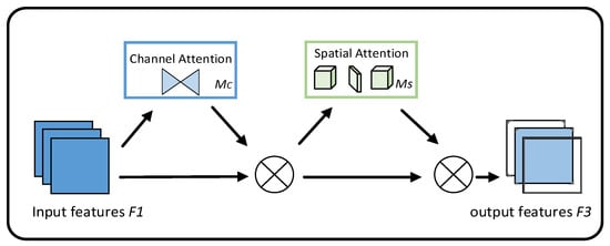
Figure 4.
The structure of GAM attention module.
The GAM module collaboratively extracts critical features through a multi-dimensional attention mechanism in dimensions such as channel, width, and height, significantly enhancing feature interaction capabilities across different dimensions [19]. By integrating it into the A2C2f module, the design improves attention allocation during branching processes, minimizes interference from irrelevant information, and boosts feature quality. This approach effectively resolves missed detection issues in PCB defect inspection systems caused by low-contrast defects.
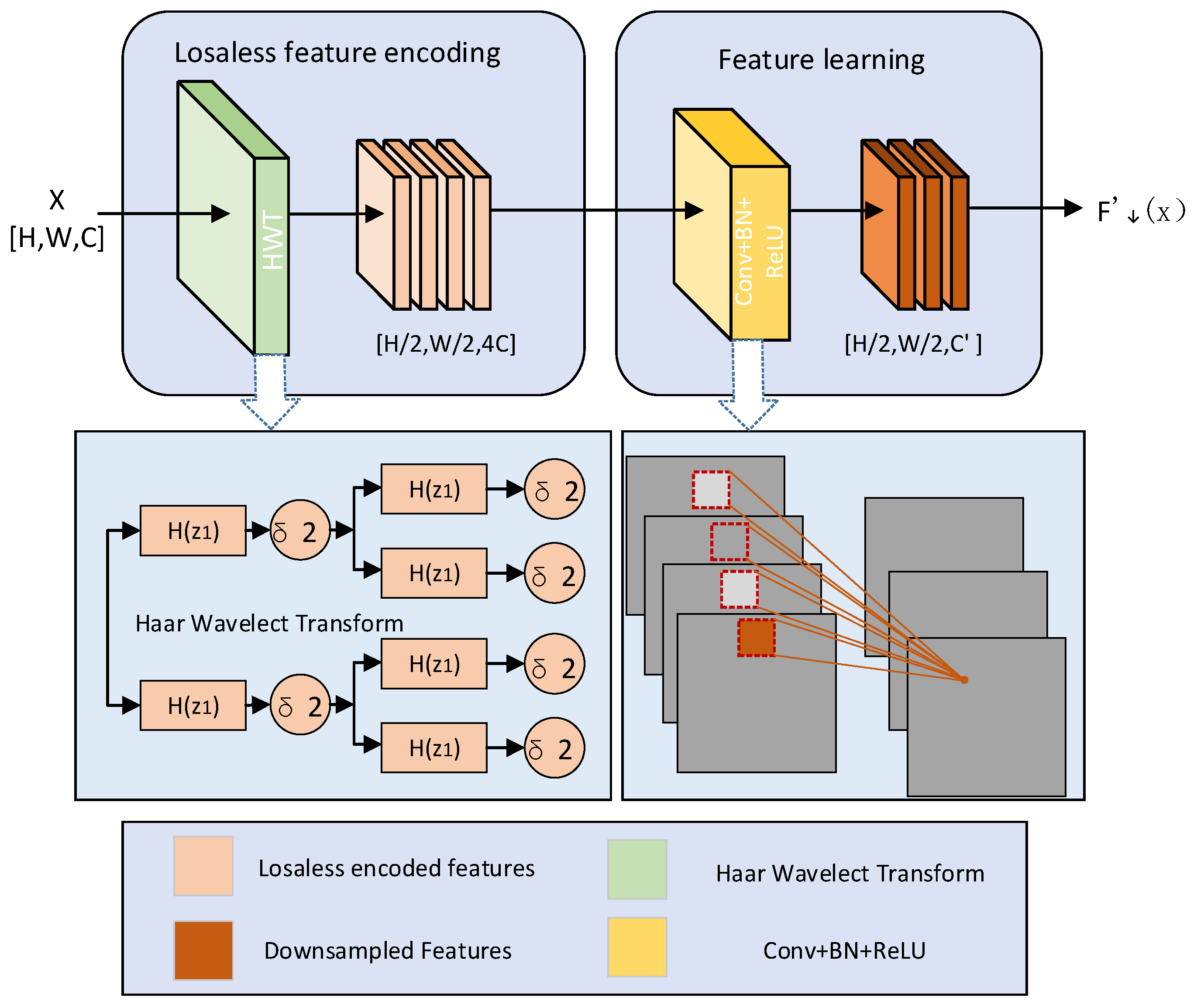
2.2.2. The Haar Wavelet Downsampling
The HWD [20] is a feature downsampling method based on the Haar wavelet transform, designed to mitigate information loss during downsampling through multi-resolution analysis. As shown in Figure 5, the module architecture of GAM is illustrated in detail. Given an input feature map , the Haar wavelet transform decomposes it into a low-frequency sub-band and high-frequency sub-bands , , and via a filter bank.
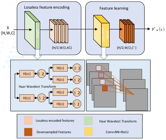
Figure 5.
The HWD module architecture.
The output feature map is constructed by channel-wise concatenation and reorganization of these sub-bands. A 1 × 1 convolution adaptively fuses multi-frequency information, reducing spatial resolution while preserving high-frequency details, thereby significantly enhancing feature representation for small object detection. The mathematical formulation is provided in Equations (9)–(12).
where represents the original feature map, sub-band preserves low-frequency components (approximation image), while sub-bands , , and isolate directional fine-grained features across lateral, longitudinal, and oblique axes, correspondingly.
In YOLOv12, the HWD module replaces traditional convolution by leveraging Haar wavelet multi-frequency decomposition to retain high-frequency details such as spur and spurious copper defects. This approach effectively mitigates feature loss during downsampling. Compared to strided convolution, its low-frequency components preserve global structural integrity while high-frequency components amplify localized anomaly responses [21], significantly enhancing both detection accuracy and robustness for small objects in industrial quality inspection scenarios.
2.2.3. The Bidirectional Feature Pyramid Network
The BiFPN [22] dynamically optimizes hierarchical feature interactions through bidirectional cross-scale connections and learnable weighted fusion of multi-resolution features. Through interconnected bidirectional cross-layer links, it enables bidirectional integration of high-level semantic information with low-level spatial details. High-level features are upsampled and fused with adjacent lower-level features, while enhanced low-level features in the reverse path undergo downsampling for secondary fusion with higher-level counterparts. Repeated bidirectional propagation strengthens cross-scale contextual awareness, with all hierarchical output feature maps collectively contributing to detection head predictions. For input feature map at hierarchical level with varying resolutions, the mathematical formulations of the bidirectional cross-layer links are defined in Equations (13) and (14), respectively. The architectural diagram is illustrated in Figure 6.
where , , , and represent learnable normalized weights, dynamically adjusted via Softmax constraints to balance the contribution of multi-resolution features.
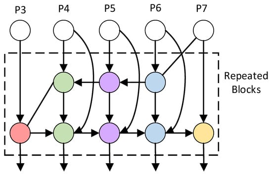
Figure 6.
The BiFPN structure.
Compared to traditional feature concatenation methods, BiFPN introduces a learnable dynamic weight allocation mechanism that adaptively adjusts channel contributions in cross-scale feature fusion, effectively eliminating noise interference and reducing feature redundancy [23]. By constructing bidirectional cross-scale connections in the Neck layer of YOLOv12, it enhances sensitivity to small objects while maintaining localization accuracy for large-scale defects, thereby strengthening the detection model’s generalization capability and inference speed.
2.2.4. The Parallel Perception Attention Detection Head
Traditional detection heads rely primarily on single-branch convolutional operations, lacking targeted optimization for complex scenarios, especially small objects. The PPA detection head significantly enhances feature representation for small objects by introducing multi-branch feature extraction and an adaptive attention mechanism, which dynamically prioritizes critical spatial and channel-wise information [24].
The input feature map is processed through three parallel branches: the local detail branch employs small convolutional kernels to capture fine-grained features, the global context branch expands the receptive field via dilated convolutions, and the long-range dependency branch models distant correlations through stacked convolutional layers, with their computational formulas defined in Equations (15)–(17), respectively.
The dynamic weighted fusion is achieved by adaptively integrating multi-branch features through learnable weights , , and , with the computational formula defined in Equation (18).
where , , and are generated by a lightweight MLP and normalized through Softmax.
The attention enhancement module consists of channel attention and spatial attention components, which compute the final output features through the formulas defined in Equations (19)–(21).
where represents the channel attention weight, denotes the sigmoid function, corresponds to the multilayer perceptron, indicates the average pooling operation, is the output feature map after multi-branch feature fusion, stands for the spatial attention weight, refers to the concatenation operation, signifies the max pooling operation, and represents channel-wise multiplication.
2.2.5. The Normalized Wasserstein Distance Loss Function
The NWD loss function [25] is a specialized measurement mechanism tailored for small object recognition, employing statistical modeling in 2D space to evaluate positional correlations. This approach demonstrates enhanced robustness against dimensional variations compared to traditional overlap-based metrics, showing particular efficacy in scenarios requiring precise alignment of minuscule visual patterns [26]. The sensitivity analysis of the NWD loss function for tiny and normal-scale objects is shown in Figure 7.
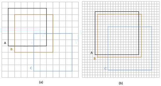
Figure 7.
The sensitivity analysis of IoU across different object scales. (a) The tiny dimension object. (b) The normal dimension object. Box A represents the ground truth bounding box, boxes B and C denote the predicted bounding boxes.
The Gaussian modeling of bounding boxes involves converting into a 2D Gaussian distribution parameterized by an ellipse, where the mean represents the center coordinates, and the covariance matrix is derived from the width and height .
For Wasserstein distance computation, the squared Wasserstein distance between two Gaussian distributions E and F is calculated as shown in Equation (22).
represents the distance vector. Since cannot be directly used as a similarity measure, an exponential normalization is applied to derive the similarity score, as formulated in Equation (23).
where is the normalization constant, typically set to the statistical average Wasserstein distance across the dataset.
The loss function is constructed by defining the final loss as , where and represent the Gaussian distributions of the predicted and ground-truth bounding boxes, respectively. By minimizing this loss, the Gaussian distributions of the predicted and ground-truth boxes are aligned, mitigating the sensitivity of IoU to positional deviations in small objects.
3. Results
To comprehensively evaluate the performance of the proposed algorithm in PCB surface defect detection tasks and the optimization efficacy of its enhancement modules, extensive experiments were conducted. Section 3.1 describes the dataset and image augmentation methods, Section 3.2 details the experimental environment, Section 3.3 introduces the performance metrics, and Section 3.4 analyzes the results through multiple experiments, validating the effectiveness of the proposed model for detecting micro-defects. Ablation studies further confirmed the rationality and effectiveness of the improved module designs.
3.1. Dataset
In this study the experimental data were derived from the publicly available PCB defect dataset PKU-Market-PCB [27], provided by the Open Lab on Human–Robot interaction of Peking University. As the primary dataset for comparative and ablation studies, it contains 1386 images covering six defect types: missing hole (Mh), mouse bite (Mb), open circuit (Oc), short circuit (Sh), spur (Sp), and spurious copper (Sc). Unlike other PCB datasets, this dataset presents distinct challenges for PCB microscopic defect detection due to uneven illumination and sparse defective samples. Following the methodology in [28], this study applied grayscale processing as well as rotation and brightness variation for image enhancement as shown in Figure 8. The rotation operation dynamically updates bounding box coordinates via an affine transformation matrix. Enhanced images with overlaid annotation boxes are visualized using LabelImg. Subsequently, the IoU values between original and transformed bounding boxes are calculated to filter out abnormal transformation results. The dataset underwent stratified random partitioning with proportional allocation ratios of 8:1:1 for training, validation, and test subsets, respectively, ensuring class distribution consistency across splits.
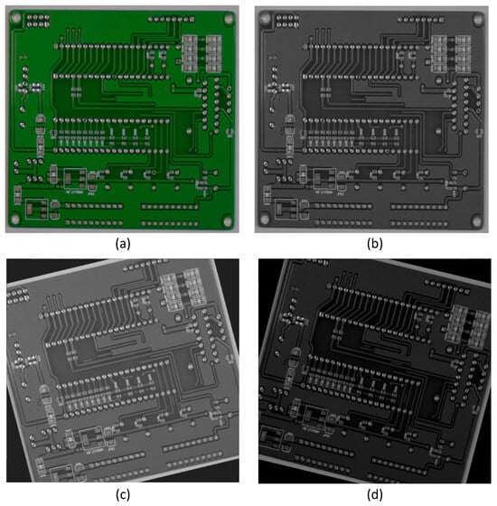
Figure 8.
The processing of image enhancement. (a) The original image. (b) The grayscale-processed image. (c) The image rotated 15 degrees to the right with brightness increased by 15%. (d) The image rotated 15 degrees to the left with brightness decreased by 15%.
3.2. Experimental Environment and Training Parameters
Table 1 systematically documents the experimental configuration, which utilized 100 training iterations with input images uniformly resized to 640 × 640 resolution and a dataset batch size of 4. The stochastic gradient descent (SGD) optimizer was deliberately selected to address the stability convergence duality characteristic of object detection frameworks, with essential hyperparameters configured through rigorous empirical validation: an initial learning rate of η = 0.01 was implemented with cyclical scheduling, momentum coefficient β = 0.937 to maintain exponentially decaying averages of past gradients, and L2 regularization applied to backbone network parameters to impose Lipschitz continuity constraints on the weight space, thereby systematically mitigating overfitting risks while preserving feature discriminability. Mosaic data augmentation was additionally incorporated to construct composite samples through image tiling, integrating multi-scale defects to significantly enhance the model’s robustness against small objects and occluded scenarios.

Table 1.
The experimental environment parameters.
3.3. Evaluation Metrics
The experiment evaluated detection performance using metrics including Precision, measuring the accuracy of positive class predictions; Recall, reflecting the coverage capability of true positive samples; mean Average Precision mAP; model parameter count; computational complexity GFLOP; and frame rate FPS. Precision quantifies the model’s accuracy in predicting positive class samples, while Recall indicates its ability to cover all true positive samples, with their formal calculations defined in Equations (24) and (25).
where TP denotes the total number of correctly detected objects; FP represents the total number of false positive detections; and FN indicates the total number of missed detections.
The mAP evaluates a model’s overall detection capability in multi-class tasks by integrating AP values of all categories, with higher mAP values indicating enlarged P-R curve areas across categories, reflecting improved detection consistency. The formal calculation is detailed in Equation (26), where is the number of categories.
The parameter count (Params) characterizes the memory footprint by aggregating trainable parameters across network layers, convolutional kernels, biases, and normalization scaling factors, while computational complexity (GFLOPs) quantifies arithmetic operation intensity during single-pass inference using billions of floating-point operations as the metric, reflecting computational resource consumption. Meanwhile, frames per second (FPS) dynamically evaluates real-time processing capabilities through completed inference cycles per temporal unit under hardware constraints.
3.4. Experimental Analysis
3.4.1. Comparison with Baseline Model
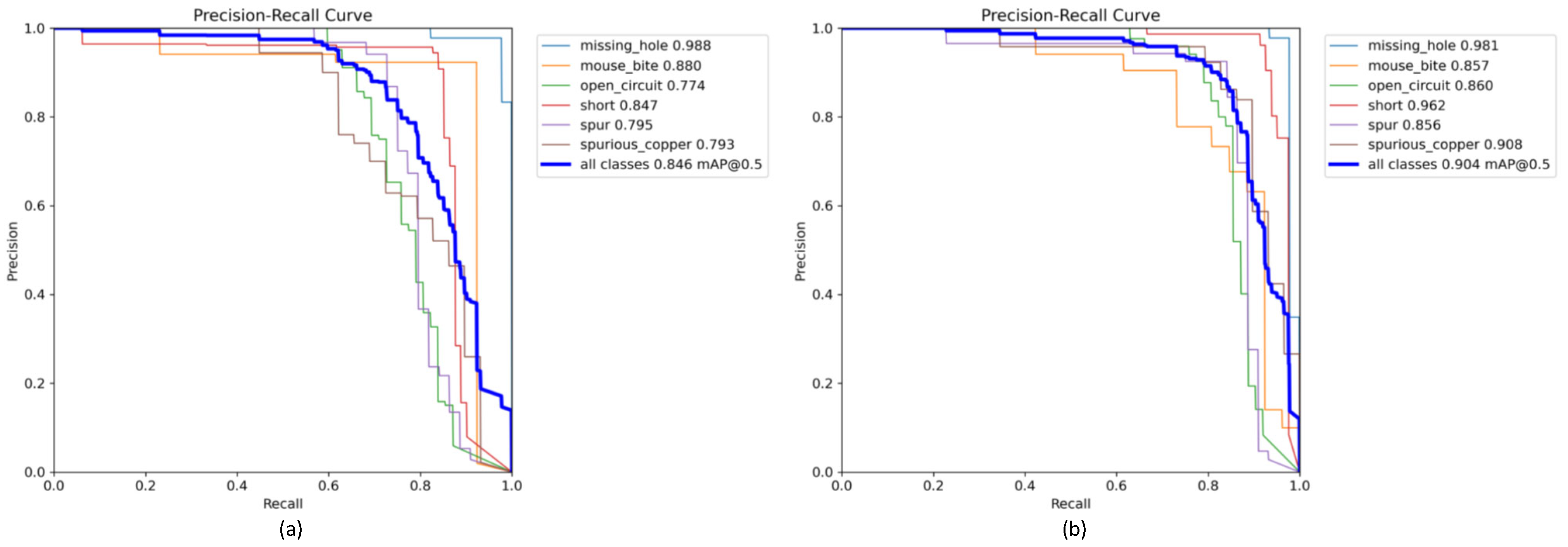
Experimental analysis compared with the baseline YOLOv12n, where the detection performance differences between the improved model and the baseline YOLOv12n are visually presented through the Precision–Recall Curve shown in Figure 9. Analysis of the Precision–Recall Curve visually reveals behavioral differences between the two models under varying object sizes.
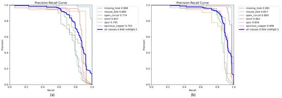
Figure 9.
Precision–Recall Curve. (a) The baseline YOLOv12n. (b) The improved model.
The experimental results shown in Figure 9 demonstrate that the proposed improved model achieves a mAP@50 of 90.4%, representing a 5.8-percentage-point absolute improvement over the baseline YOLOv12n model’s 84.6%, which fully validates the precision advantage of the enhanced solution in complex defect detection tasks. For six distinct defect categories, the improved model exhibits only marginal mAP value decreases of 0.7% and 2.3%, respectively, for detecting medium-to-large objects like missing holes and mouse bites compared to YOLOv12n, indicating that the attention mechanisms preserve localization accuracy for large objects. Significant enhancements are observed in detecting open circuits, short circuits, spur, and spurious copper defects, with the most notable improvement being an 11.5% AP increase for spurious copper detection, thoroughly demonstrating the technical superiority of multi-module collaborative optimization in micro-feature extraction and effectively confirming the high-precision detection capability of the proposed model for minuscule defects.
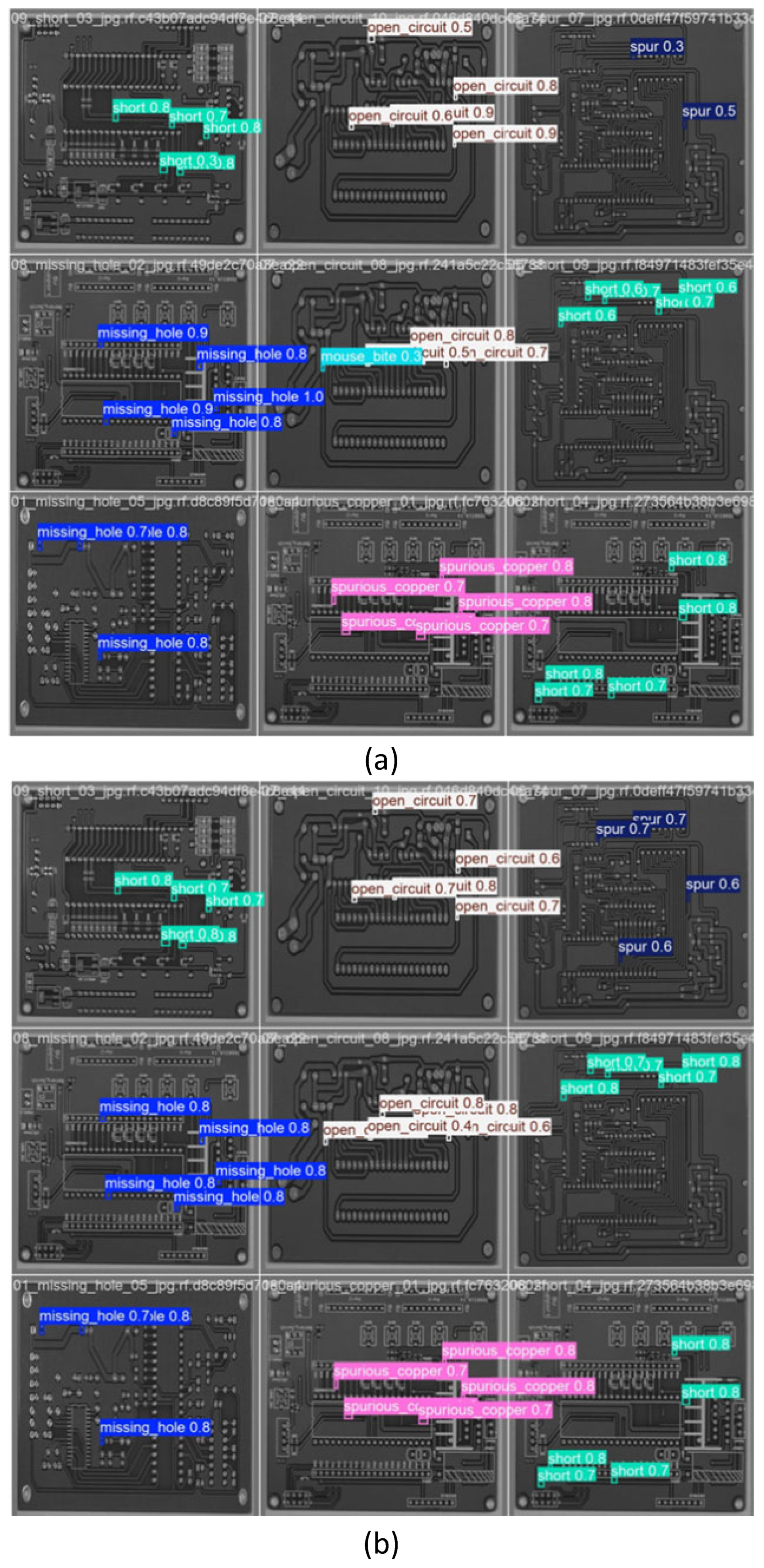
Figure 10 presents visual detection result comparisons between the improved model and the YOLOv12n baseline model for PCB surface defect inspection, where the enhanced model demonstrates zero missed detections for spur defect categories and eliminates false detections in mouse bite defects compared to the baseline, effectively validating the robust detection performance of the proposed improvements for micro-defects in high-precision PCB inspection scenarios.
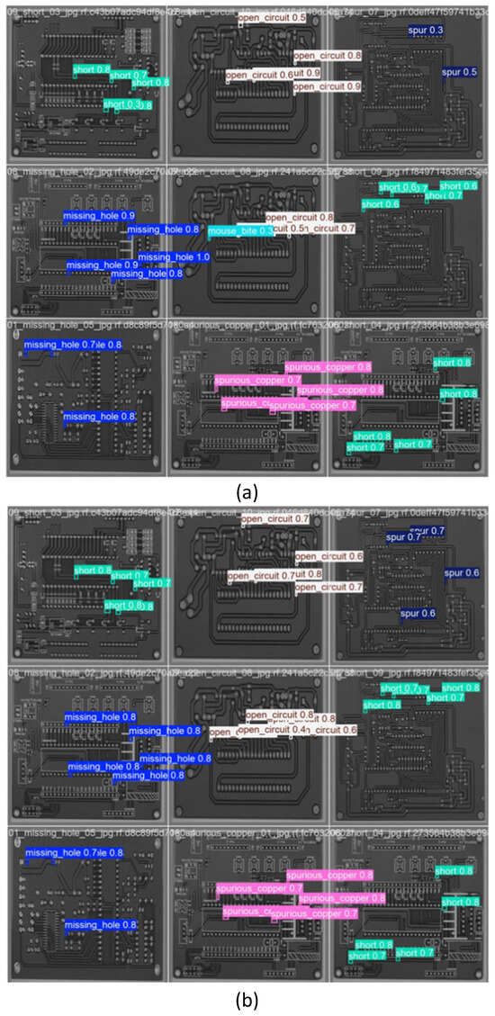
Figure 10.
Visual comparison of the detection effect. (a) The baseline YOLOv12n. (b) The improved model.
3.4.2. Comparison of Object Detection Models
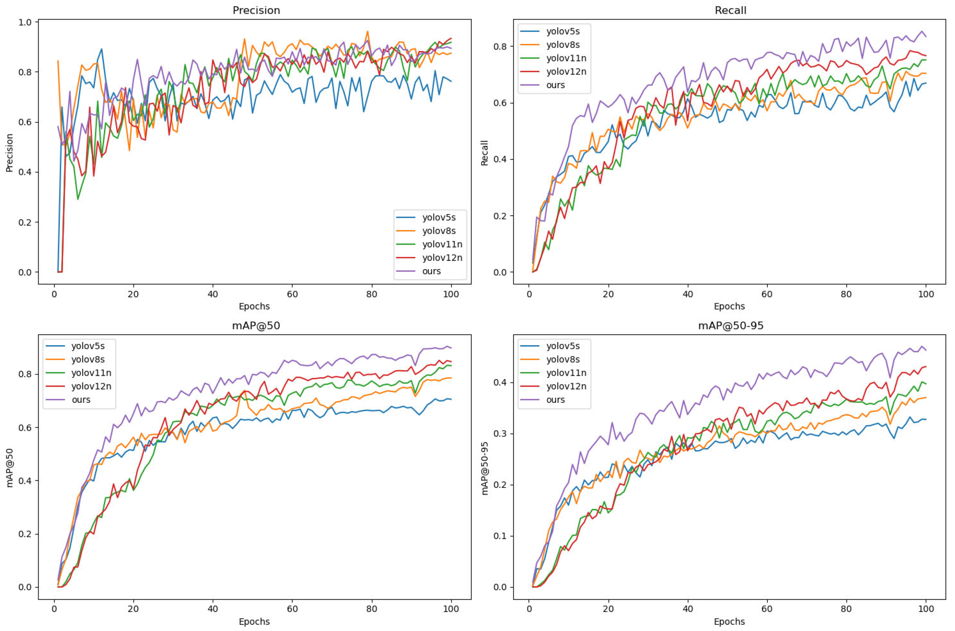
While YOLO series algorithms have achieved efficient detection in PCB defect inspection through their end-to-end regression architecture, they face challenges with increased missed detection rates in scenarios involving dense micro-objects. This study conducted comprehensive comparative experiments with other object detection algorithms [29,30,31,32,33], on the PKU-Market-PCB dataset, with visual comparative results illustrated in Figure 11 and detailed quantitative data provided in Table 2 and Table 3.
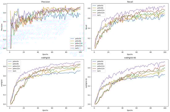
Figure 11.
Comparison with the results of mainstream YOLO models.
Table 2.
Comparison of AP for each defect and overall mAP across different models.
Table 3.
Comparison of model complexity and stability of different models.
Figure 11 visually demonstrates that the improved model consistently outperforms other models in precision, recall, mAP@50, and mAP@50:90 during training. As evidenced by Table 2, the enhanced model exhibits the most significant improvement in the spurious copper category, achieving 90.8% detection accuracy with performance gains of 28.1%, 1.1%, 19.6%, 3.0%, and 6.9% over Faster R-CNN, RT-DETR-R18, YOLOv5s, YOLOv8s, and YOLOv11n, respectively, indicating that the multi-module collaborative optimization in the proposed framework substantially strengthens feature representation capabilities for micro-defects, delivering superior detection efficacy in micron-level defect inspection scenarios. Based on Table 3, the improved model achieves 3.87 M parameters and 72.8 FPS, demonstrating lower computational complexity and faster inference speed compared to Faster R-CNN, RT-DETR-R18, and mainstream YOLO models. Relative to the baseline YOLOv12n model, it exhibits a 0.61 M increase in Parameters, a 1.6 G increase in FLOPs, and only a 4.7% reduction in FPS, indicating that while achieving high accuracy, YOLOv12n’s increased Parameters and FLOPs restrict its inference speed.
3.4.3. Comparison of GAM with Other Attention Mechanisms
To validate the feature selection efficacy of the GAM attention mechanism in PCB surface defect detection, this study systematically compares it with mainstream attention modules including SE, CA, ECA, and CBAM through comprehensive experimental analysis containing micro-object defects, with the comparative results detailed in Table 4.
Table 4.
Comparison of effects of different attention mechanisms.
As shown in Table 4, the GAM attention mechanism outperforms traditional attention methods such as SE, ECA, CA, and CBAM in terms of mAP, parameter count, computational efficiency, and inference speed. Specifically, it achieves 2.1%, 1.3%, 1.8%, and 1.0% higher mAP compared to SE, ECA, CA, and CBAM, respectively. Experiments reveal that conventional methods, constrained by static architectures or localized interactions, tend to exhibit feature attenuation or confusion in scenarios involving dense components or noise interference. By collaboratively optimizing channel spatial feature interactions through cross-layer gating mechanisms and deformable convolutional kernels, the GAM attention mechanism effectively enhances detection sensitivity to micron-level defects, significantly improves the robustness for small object defect recognition, and highlights its comprehensive performance advantages in PCB defect detection tasks.
3.4.4. Comparison of the HWD with Other Convolutional Modules
To validate the performance advantages of the HWD downsampling module in feature preservation and computational efficiency optimization, this study conducted comparative experiments with three representative convolutional modules: AKConv, DWConv, and DSConv; the experimental results are summarized in Table 5.
Table 5.
Comparison of effects of different convolutional modules.
As shown in Table 5, after integrating the HWD downsampling module, the mAP values are consistently higher than those of other convolution modules, specifically 0.95%, 1.7%, and 1.4% higher than AKConv, DWConv, and DSConv, respectively. Comparative experiments demonstrate that the HWD downsampling module preserves the geometric structures of object contours while suppressing high-frequency noise through hierarchical feature reorganization and channel compression. Its dynamic weighting strategy, in contrast to the computational intensity of AKConv, the local limitations of DWConv, and the static parameters of DSConv, more effectively preserves information across deep and shallow layers. Additionally, it ensures more stable structural updates during gradient backpropagation.
3.4.5. Ablation Experiment
This study systematically validated the model’s superior performance for detecting tiny PCB surface defects through phased ablation experiments combining optimized modules. The experiments quantitatively evaluated the impact of five key improvement strategies—GAM, HWD, BiFPN, PPA, and NWD—on the detection metrics for six defect categories, including average precision per class and overall detection efficiency, as shown in Table 6. The results demonstrate that each strategy applied to the baseline model enhanced detection performance at varying degrees, with significant accuracy improvements for small objects. Here, A, B, C, D, and E represent the GAM attention mechanism, HWD downsampling module, BiFPN bidirectional feature pyramid network, PPA small object detection head, and NWD loss function, respectively.
Table 6.
Ablation experiment results.
Ablation experiments demonstrate that the introduced GAM attention mechanism effectively focuses on critical feature regions to strengthen semantic perception, improving mAP by 3.0%; the integration of the HWD downsampling module maintains feature integrity through hierarchical compression while optimizing computational efficiency, elevating mAP by 2.0%; the BiFPN bidirectional feature pyramid enhances multi-scale detection by reconstructing cross-scale feature fusion paths, boosting mAP by 2.5%; the PPA small object detection head specifically reinforces detail perception to overcome micro-defect recognition bottlenecks, increasing mAP by 2.2%; and the NWD loss function significantly improves localization accuracy by refining bounding box matching criteria, raising mAP by 1.3%. These improvements collectively form a synergistic optimization framework that systematically addresses core challenges in PCB surface defect detection, feature extraction, scale adaptation, micro-object capture, and localization errors, through step-by-step decoupling and resolution.
Experiments 8, 11, 14, and 15 demonstrated significant synergistic optimization effects on feature representation capabilities for both large and small objects after introducing the BiFPN bidirectional feature pyramid network. Experiments 9, 12, and 14, based on different improved models incorporating the PPA attention detection head, showed markedly enhanced detection accuracy for spur and spurious copper defects, validating the effectiveness of the PPA module in boosting small object detection precision. The inclusion of the NWD loss function improved detection accuracy across all models to varying degrees, with the greatest mAP improvement observed for spurious copper, indicating that NWD enhances bounding box regression accuracy in small object recognition, thereby strengthening overall model performance.
4. Discussion
The experiment results collectively demonstrate that the multidimensional improvement strategies proposed in this study exhibit deep synergistic optimization effects in PCB defect detection tasks. By adopting a multi-module optimization architecture, applying PCB specific image data augmentation techniques, and designing optimized loss functions, the feature representation capability for micro-defects has been significantly enhanced. Compared with the baseline model YOLOv12n, mAP@50 and mAP@50:95 increased by 5.8% and 3.9%, respectively, effectively validating the model’s high-precision detection performance specifically for microscopic defects.
Although the improved model proposed in this study enhances detection accuracy for small object PCB defects through sophisticated feature fusion strategies, the increased computational complexity adversely affects its real-time performance on resource-constrained embedded devices. In practical industrial PCB quality inspection scenarios, stringent requirements for detection speed could constrain further expansion of model complexity, necessitating a more optimal balance between precision and efficiency. Future research will therefore prioritize lightweight design and stability enhancements to strengthen the model’s effectiveness and practicality in industrial PCB defect detection applications.
Author Contributions
Conceptualization, Z.C. and B.L.; methodology, Z.C.; software, Z.C.; validation, Z.C. and B.L.; formal analysis, Z.C.; investigation, Z.C.; resources, Z.C.; data curation, Z.C.; writing—original draft preparation, Z.C.; writing—review and editing, Z.C. and B.L.; visualization, Z.C. and B.L.; supervision, Z.C. and B.L.; project administration, B.L. All authors have read and agreed to the published version of the manuscript.
Funding
This research received no external funding.
Institutional Review Board Statement
This study used public data instead of private data.
Data Availability Statement
This study utilizes public data sourced from the Peking University Open Lab for Human-Robot Interaction: https://robotics.pkusz.edu.cn/resources/dataset/, accessed on 20 January 2025.
Acknowledgments
We would like to thank the anonymous reviewers for their constructive and valuable suggestions on the earlier drafts of this manuscript.
Conflicts of Interest
The authors declare no conflicts of interest.
References
- Zhao, W.; Xu, J.; Fei, W.; Liu, Z.; He, W.; Li, G. The reuse of electronic components from waste printed circuit boards: A critical review. Environ. Sci. Adv. 2023, 2, 196–214. [Google Scholar] [CrossRef]
- Saqib, Q.M.; Mannan, A.; Noman, M.; Chougale, M.Y.; Patil, C.S.; Ko, Y.; Kim, J.; Patil, S.R.; Yousuf, M.; Shaukat, R.A.; et al. Miniaturizing power: Harnessing micro-supercapacitors for advanced micro-electronics. Chem. Eng. J. 2024, 490, 151857. [Google Scholar] [CrossRef]
- Sankar, V.U.; Lakshmi, G.; Sankar, Y.S. A review of various defects in PCB. J. Electron. Test. 2022, 38, 481–491. [Google Scholar] [CrossRef]
- He, X.; Huang, L.; Xiao, M.; Yu, C.; Li, E.; Shao, W. Investigation on the new reliability issues of PCB in 5G millimeter wave application. Microelectron. Int. 2024, 41, 130–141. [Google Scholar] [CrossRef]
- Pham, T.T.A.; Thoi, D.K.T.; Choi, H.; Park, S. Defect detection in printed circuit boards using semi-supervised learning. Sensors 2023, 23, 3246. [Google Scholar] [CrossRef]
- Abd Al Rahman, M.; Mousavi, A. A review and analysis of automatic optical inspection and quality monitoring methods in electronics industry. IEEE Access 2020, 8, 183192–183271. [Google Scholar]
- Chen, X.; Wu, Y.; He, X.; Wu, Y. A comprehensive review of deep learning-based PCB defect detection. IEEE Access 2023, 11, 139017–139038. [Google Scholar] [CrossRef]
- Zhou, Y.; Yuan, M.; Zhang, J.; Ding, G.; Qin, S. Review of vision-based defect detection research and its perspectives for printed circuit board. J. Manuf. Syst. 2023, 70, 557–578. [Google Scholar] [CrossRef]
- Wang, J.; Xie, X.; Liu, G.; Wu, L. A Lightweight PCB Defect Detection Algorithm Based on Improved YOLOv8-PCB. Symmetry 2025, 17, 309. [Google Scholar] [CrossRef]
- Zhou, G.; Yu, L.; Su, Y.; Xu, B.; Zhou, G. Lightweight PCB defect detection algorithm based on MSD-YOLO. Clust. Comput. 2024, 27, 3559–3573. [Google Scholar] [CrossRef]
- Tang, Y.; Liu, R.; Wang, S. YOLO-SUMAS: Improved Printed Circuit Board Defect Detection and Identification Research Based on YOLOv8. Micromachines 2025, 16, 509. [Google Scholar] [CrossRef] [PubMed]
- Yuan, Z.; Tang, X.; Ning, H.; Yang, Z. LW-YOLO: Lightweight Deep Learning Model for Fast and Precise Defect Detection in Printed Circuit Boards. Symmetry 2024, 16, 418. [Google Scholar] [CrossRef]
- Ji, L.; Huang, C.; Li, H.; Han, W.; Yi, L. MS-DETR: A real-time multi-scale detection transformer for PCB defect detection. Signal Image Video Process. 2025, 19, 203. [Google Scholar] [CrossRef]
- Zeng, N.; Wu, P.; Wang, Z.; Li, H.; Liu, W.; Liu, X. A small-sized object detection oriented multi-scale feature fusion approach with application to defect detection. IEEE Trans. Instrum. Meas. 2022, 71, 3507014. [Google Scholar] [CrossRef]
- Tian, Y.; Ye, Q.; Doermann, D. Yolov12: Attention-centric real-time object detectors. arXiv 2025, arXiv:2502.12524. [Google Scholar]
- Yan, C.; Zhang, H.; Ye, F.; Xu, W. Performance Analysis of Glass Surface Detection Based on the YOLOs. Curr. Sci. 2025, 5, 1679–1693. [Google Scholar] [CrossRef]
- Alif, M.A.R.; Hussain, M. YOLOv12: A Breakdown of the Key Architectural Features. arXiv 2025, arXiv:2502.14740. [Google Scholar]
- Liu, Y.; Shao, Z.; Hoffmann, N. Global attention mechanism: Retain information to enhance channel-spatial interactions. arXiv 2021, arXiv:2112.05561. [Google Scholar]
- Liu, J.; Kang, B.; Liu, C.; Peng, X.; Bai, Y. YOLO-BFRV: An Efficient Model for Detecting Printed Circuit Board Defects. Sensors 2024, 24, 6055. [Google Scholar] [CrossRef]
- Xu, G.; Liao, W.; Zhang, X.; Li, C.; He, X.; Wu, X. Haar wavelet downsampling: A simple but effective downsampling module for semantic segmentation. Pattern Recognit. 2023, 143, 109819. [Google Scholar] [CrossRef]
- Wang, W.; Li, L.; Qu, Z.; Yang, X. Enhanced damage segmentation in RC components using pyramid Haar wavelet downsampling and attention U-net. Autom. Constr. 2024, 168, 105746. [Google Scholar] [CrossRef]
- Tan, M.; Pang, R.; Le, Q.V. Efficientdet: Scalable and efficient object detection. In Proceedings of the IEEE/CVF Conference on Computer Vision and Pattern Recognition, Seattle, WA, USA, 13–19 June 2020; pp. 10781–10790. [Google Scholar]
- Shi, P.; He, Q.; Zhu, S.; Li, X.; Fan, X.; Xin, Y. Multi-scale fusion and efficient feature extraction for enhanced sonar image object detection. Expert Syst. Appl. 2024, 256, 124958. [Google Scholar] [CrossRef]
- Tang, G.; Zhao, H.; Claramunt, C.; Zhu, W.; Wang, S.; Wang, Y.; Ding, Y. PPA-Net: Pyramid pooling attention network for multi-scale ship detection in SAR images. Remote Sens. 2023, 15, 2855. [Google Scholar] [CrossRef]
- Wang, J.; Xu, C.; Yang, W.; Yu, L. A normalized Gaussian Wasserstein distance for tiny object detection. arXiv 2021, arXiv:2110.13389. [Google Scholar]
- Xu, C.; Wang, J.; Yang, W.; Yu, H.; Yu, L.; Xia, G. Detecting tiny objects in aerial images: A normalized Wasserstein distance and a new benchmark. ISPRS J. Photogramm. Remote Sens. 2022, 190, 79–93. [Google Scholar] [CrossRef]
- Huang, W.; Wei, P.; Zhang, M.; Liu, H. HRIPCB: A challenging dataset for PCB defects detection and classification. J. Eng. 2020, 13, 303–309. [Google Scholar] [CrossRef]
- Tang, J.; Yang, Y.; Hou, B.; Hao, C. PCB Defect Detection Algorithm Based on YT-YOLO. In Proceedings of the 35th Chinese Control and Decision Conference, Yichang, China, 20–22 May 2023; pp. 976–981. [Google Scholar]
- Khanam, R.; Hussain, M. What is YOLOv5: A deep look into the internal features of the popular object detector. arXiv 2024, arXiv:2407.20892. [Google Scholar]
- Yaseen, M. What is YOLOv8: An in-depth exploration of the internal features of the next-generation object detector. arXiv 2024, arXiv:2408.15857. [Google Scholar]
- Khanam, R.; Hussain, M. Yolov11: An overview of the key architectural enhancements. arXiv 2024, arXiv:2410.17725. [Google Scholar]
- Ren, S.; He, K.; Girshick, R.; Sun, J. Faster R-CNN: Towards real-time object detection with region proposal networks. IEEE Trans. Pattern Anal. Mach. Intell. 2016, 39, 1137–1149. [Google Scholar] [CrossRef]
- Zhao, Y.; Lv, W.; Xu, S.; Wei, J.; Wang, G.; Dang, Q.; Liu, Y.; Chen, J. Detrs beat yolos on real-time object detection. arXiv 2024, arXiv:2304.08069. [Google Scholar]


Disclaimer/Publisher’s Note: The statements, opinions and data contained in all publications are solely those of the individual author(s) and contributor(s) and not of MDPI and/or the editor(s). MDPI and/or the editor(s) disclaim responsibility for any injury to people or property resulting from any ideas, methods, instructions or products referred to in the content. |
© 2025 by the authors. Licensee MDPI, Basel, Switzerland. This article is an open access article distributed under the terms and conditions of the Creative Commons Attribution (CC BY) license (https://creativecommons.org/licenses/by/4.0/).