1. Introduction
Power electronics technologies are advancing rapidly to meet the growing demands for greater efficiency, reliability, and power quality. Among these advancements, multilevel inverters (MLIs) have emerged as a key innovation, offering substantial advantages over traditional two-level inverters, particularly in high-power and high-voltage applications. MLIs are designed to create a stepped output voltage that closely resembles a smooth sine wave, which greatly lowers harmonic distortion, reduces electromagnetic interference (EMI), and boosts the overall system efficiency. These characteristics make MLIs highly beneficial in various applications, including renewable energy systems, electric vehicles (EVs), industrial motor drives, and grid-connected energy systems [
1,
2,
3].
The growing emphasis on renewable energy and electric vehicles has further elevated the importance of MLIs. In renewable energy systems such as those using solar and wind power, MLIs are crucial in converting the generated direct current (DC) into an alternating current (AC) compatible with the power grid. Generating a high-quality output voltage with minimal harmonic distortion ensures seamless integration with the grid. In electric vehicles, MLIs drive motors, providing advantages such as a higher power density, increased efficiency, and precise control over the motor performance [
4].
Despite the numerous benefits offered by MLIs, challenges remain in their design and implementation phases. These challenges include the complexity of selecting appropriate topologies, maintaining the voltage balance, and developing efficient control strategies. Researchers and engineers are focusing on developing innovative topologies, advanced control algorithms, and next-generation semiconductor materials to address these challenges. In particular, the adoption of wide-bandgap (WBG) semiconductor materials such as silicon carbide (SiC) and gallium nitride (GaN) has been a game-changer in MLI technology. These materials significantly improve the system efficiency by enabling higher switching frequencies, reducing energy losses, and offering better thermal performance [
5]. Specifically, SiC devices have been shown to reduce switching losses by up to 50%, enhancing the system’s overall performance. These devices also operate with higher switching frequencies and generate less heat, which results in improved efficiency and compact system designs. Using SiC and GaN in dynamic multilevel inverters further improves the energy conversion efficiency and facilitates the design of more cost-effective, scalable systems. A thorough study by Ruiqing Cheng and his team (2019) looked at how SiC and GaN devices enhance the performance of multilevel inverters, giving a complete overview of how they affect switching losses and efficiency [
6].
Also, using optimization algorithms and machine learning (ML) methods is becoming more common to make MLIs work better in real time, find problems faster, and set up systems for predicting maintenance needs. AI-based control algorithms make energy use more efficient by allowing for faster reactions to changes in how things are working, which is important for keeping performance steady when loads and environmental conditions change. Moreover, advancements in virtual modeling, such as the use of digital twin technology [
7], are accelerating the design and testing processes, which allows for faster development cycles and more efficient system integration.
Looking ahead, MLI technology is progressing toward more modular and scalable designs. Modern systems, such as cascaded H-bridge (CHB) and flying capacitor topologies, offer increased reliability by providing higher fault tolerance and redundancy. These advanced topologies also improve the system’s flexibility and performance, especially in applications that require high availability and robustness. Furthermore, integrating MLIs with innovative grid systems will enhance coordination with distributed energy resources and energy storage systems, enabling more efficient and dynamic energy distribution [
8]. Although traditional multilevel inverters (MLIs) offer several advantages, some significant limitations restrict their performance, especially in high-power and high-voltage applications:
Complex Design and Control Structures: Traditional MLIs require multiple switching devices and complex control algorithms. This increases the complexity of both the design and control of the inverters. At higher power levels, the control strategies become more intricate, which complicates the optimization processes necessary to ensure system accuracy. Additionally, the use of high-quality components can lead to increased costs [
3].
Switching Losses and Efficiency Issues: Switching losses in traditional MLIs have a considerable impact on efficiency. As the switching frequencies increase, these losses tend to rise, leading to thermal management problems. This can adversely affect the overall efficiency and reliability of the system [
9].
Harmonic Distortion: MLIs are designed to generate an ideal sinusoidal output voltage. However, when low-quality components are used, harmonic distortion can occur. This can degrade the power quality and lead to issues such as electromagnetic interference (EMI), which can hurt the system’s performance [
10].
High Cost: The use of numerous switching elements and components in MLI systems can increase the overall system cost. In industrial applications and those requiring high power, the hardware costs of MLIs can be significantly higher compared to those of traditional inverters [
11]. Overcoming these limitations is crucial for improving energy efficiency, reducing costs, and ensuring the reliability of the system.
This paper reviews the current state of multilevel inverter technology, examining its various topologies, modulation techniques, and applications. It highlights recent advancements in these areas and their transformative impact on power conversion systems. Through this study, the significant contributions of MLIs to the field of power electronics are made clear, illustrating their role in driving forward the development of sustainable energy solutions. Ongoing research and technological advancements are set to further enhance the efficiency, reliability, and adaptability of MLIs, ensuring that they remain a pivotal technology in modern power systems.
Understanding that all scientific work should enrich the reader’s knowledge, this study aims to bridge gaps in the existing literature regarding MLI development and provide new insights and methodologies. It comprehensively reviews recent advancements in various MLI topologies, modulation techniques, and emerging applications, contributing valuable knowledge to academic research and industrial practices. This paper presents these innovations, emphasizing their significant impact on the scientific community and real-world applications.
2. Multilevel Inverters
Multilevel inverters (MLIs) create an alternating current (AC) output voltage in several steps, which leads to less distortion and better quality than those provided by regular two-level inverters. This property has rendered MLIs highly favorable in medium- and high-voltage applications and high-power contexts. Although conventional two-level inverters are favored for low-voltage applications owing to their high switching frequencies and voltage tolerance constraints, multilevel inverters excel in high-power and -voltage scenarios [
12].
The fundamental working idea of MLIs is to provide a high-power output voltage by using many low-voltage DC levels, thereby minimizing the voltage stress on each semiconductor switching component. This method enhances the system’s overall efficiency and reduces switching losses. Moreover, MLI topologies provide compact configurations requiring reduced spatial requirements and lower installation costs and confer benefits like enhanced modularity, less complexity, and fewer components [
13].
Another significant benefit of MLIs is their ability to generate high voltage levels with little harmonic distortion, obviating the need for large and expensive transformers. These characteristics render MLIs essential across various applications, including photovoltaic (PV) systems, wind energy conversion systems, fuel cells, electric vehicles, induction motor drives, active power filters, wireless power transfer, high-voltage direct current (HVDC) transmission, and flexible alternating current transmission systems (FACTSs) [
14].
The input supply of MLIs is typically direct current (DC) energy sourced from wind turbines, solar panels, fuel cells, or energy storage devices. The multilevel structure of an MLI converts this DC energy into a high-quality AC output. Classic multilevel inverter topologies are categorized as diode-clamped, flying capacitor, and cascaded H-bridge inverters. Specific benefits and constraints in various application domains distinguish each of these topologies. The subsequent sections will elaborate on a thorough examination and comparison of these topologies.
The exceptional attributes provided by MLIs have resulted in their growing utilization in contemporary energy systems and industrial applications. The significance of MLIs is growing, particularly in domains such as renewable energy integration, energy efficiency, and electric mobility. This paper aims to explain the current state and future potential of this technology by closely examining the basic ideas, designs, and control methods related to MLIs and the areas where MLIs are used.
Figure 1 depicts conventional multilevel inverters, and their key features are further examined in the following subsections.
In multilevel converter topologies, three voltage levels are typically considered the minimum. By incorporating bidirectional switches, a multilevel voltage-source converter can operate as both a rectifier and an inverter. In such cases, “converter” is often used instead of “inverter” to reflect this dual function. These converters can switch their input or output nodes between multiple voltage or current levels, surpassing the basic two levels.
Figure 2 shows the switching variation of the inverter according to the number of levels.
Figure 2a illustrates the two-level,
Figure 2b the three-level, and
Figure 2c the m-level single-phase inverter output switching states.
As the number of voltage levels increases, the output’s Total Harmonic Distortion (THD) approaches zero, resulting in a cleaner, more sinusoidal waveform. However, the number of achievable voltage levels is limited by factors such as the voltage imbalance, the need for voltage-clamping elements, the circuit design complexity, the controller’s packaging constraints, and the associated capital and maintenance costs.
To minimize the THD and produce a pure sinusoidal voltage waveform, particularly for nonlinear loads, the design of the output filter is essential. The output filter plays a critical role in shaping the waveform by attenuating high-frequency harmonics, ensuring that the output voltage closely resembles a pure sine wave. The design process involves selecting appropriate components, such as inductors and capacitors, to achieve the desired harmonic attenuation and bandwidth. These calculations also consider the load characteristics, the switching frequency of the converter, and the harmonic profile generated by the nonlinear load. By carefully designing the output filter, the THD can be minimized, improving efficiency and reliability. Moreover, the design must balance factors such as the size, cost, and performance to ensure that the converter meets technical requirements while being economically feasible. The output voltage waveform formula for multi-level inverter specifications is given in
Figure 3.
2.1. Cascaded H-Bridge Multilevel Inverters
Baker and Bannister introduced the first multilevel inverter structure in 1975. However, the cascade H-bridge inverter was fully developed and patented by Lai and Peng in 1996. Their design improved Baker’s model by adding an anti-parallel diode and explaining the three-phase circuit structure.
Due to its modular structure and flexibility, the cascaded H-bridge multilevel inverter (CHB-MLI) is widely used in high-power applications, particularly in flexible alternating current transmission systems (FACTSs) control. This topology combines multiple isolated voltage levels to achieve a near-sinusoidal waveform at the inverter output. Adding more H-bridges can increase the reactive power without redesigning the power stage, and built-in redundant H-bridges provide fault tolerance. Additionally, this topology ensures phase balancing, a feature not available in common DC bus topologies. Its cell-based structure allows for the easy scaling of the voltage and power levels.
The converter topology is based on the series connection of single-phase inverters with discrete DC sources. In this case, at least two full-bridge inverters are required to realize the cascading concept. Using K units of H-bridge inverters, a cascade-connected H-bridge inverter with m = 2k + 1 levels can be created (m represents the number of levels). Each module is powered by an isolated DC voltage source, as shown in
Figure 4a, and consists of four semiconductor elements. A single full-bridge inverter can produce three voltage levels: +V
DC, −V
DC, and 0 volts. The output voltage waveform of a single-phase full-bridge inverter is demonstrated in
Figure 4b.
Figure 5 shows the circuit structure of a five-level CHB-MLI, while
Figure 6a–c show the upper module, lower module, and inverter total output voltage waveforms, respectively. The switching states for the five-level CHB-MLI are given in
Table 1, demonstrating the level concept.
2.2. Diode-Clamped Multilevel Inverters
The most-used multilevel topology is the diode-clamped multilevel inverter (DCMLI), in which diodes clamp the DC bus voltage to achieve a multilevel waveform. The diode-clamped multilevel inverter (DCMLI) was derived from the cascade inverter in 1980 [
10]. The first proposed diode-clamped inverter was a three-level inverter. The neutral-point-clamped (NPC) inverter is a diode-clamped inverter [
16]. The initial application of this topology was implemented in 1981 using Pulse Width Modulation (PWM) [
17].
Increasing the number of voltage levels improves the output voltage quality, causing the voltage waveform to more closely resemble a sinusoidal waveform. However, in high-level inverters, capacitor voltage balancing becomes a critical issue. When the levels are sufficiently high, the voltage of diodes and switching elements will increase, rendering the system impractical. If an inverter operates under PWM conditions, the reverse blocking voltage of the clamping diodes becomes the primary design challenge.
In a five-level diode-clamped inverter, the voltage across each capacitor is V
DC/4. We take the midpoint of the capacitors connected to the DC voltage as neutral, thereby obtaining negative voltages.
Table 2 shows the relationship between the output voltage of a five-level diode-clamped inverter and the open/closed state of the switch.
Figure 7 illustrates the topologies of three-level and five-level diode-clamped multilevel inverters. As shown in
Figure 7a, a three-level diode-clamped multilevel inverter consists of two complementary switch pairs and two clamping diodes. Each switch pair operates in a complementary mode, while the clamping diodes provide access to the midpoint voltage.
In a three-level inverter, each phase shares a common DC bus, divided into three voltage levels by two DC capacitors (C
1 and C
2). The DC bus voltage (VDC) is split into three levels using the series connection of these capacitors: +V
DC/2, 0, and −V
DC/2. The clamping diodes (D
1 and D
1’) limit the voltage stress across each switching device to V
DC/2. The inverter’s output voltage (Van) can take three values: +V
DC/2, 0, and −V
DC/2 [
17]. Two switches conduct at any given time in a three-level inverter, whereas in a five-level inverter, four switches conduct simultaneously. This pattern continues as the number of levels increases.
In a diode-clamped inverter setup, the output voltage (Van) is measured between points a and n, which shows the AC voltage from the phase to neutral. The voltage between points a and 0 (Va0) shows the DC voltage from the phase to ground. If the output voltage is measured from points a-0 instead of a-n, the inverter works like a DC/DC converter.
The diode-clamped multilevel inverter topology uses clamping diodes with different reverse blocking voltages. For instance, diode D1’ blocks 3 VDC/4, diodes D2 and D2’ block 2 2VDC/4, and diode D3 blocks 3 VDC/4. These diodes clamp VDC/4, 2 VDC/4, and VDC/4 from the DC bus voltage (VDC) to the output.
Practical applications introduce a time limit for the switching signals of complementary switch pairs. This time limit ensures that both switches in a complementary pair are turned off briefly, reducing switching losses and minimizing the risk of short circuits.
2.3. Flying Capacitor Multilevel Inverters
The flying capacitor multilevel inverter, also known as the capacitor-clamped multilevel inverter, made its debut in 1992 [
18]. The difference between the capacitor clamp inverter topology and the diode clamp topology is that capacitors are used instead of diodes. Each capacitor leg has a voltage that determines each step’s voltage level.
Figure 8 shows capacitor clamp multilevel inverter schematic diagrams for three and five levels.
A three-level capacitor-clamped inverter will generate three different voltage levels between terminals a and n: Van = +V
DC/2, 0, and −V
DC/2. Turning on switches S
1 and S
1’ charges the clamping capacitor C
1, while turning on switches S
2 and S
2’ discharges capacitor C
1, determining the charge balance of capacitor C
1. Capacitor-clamped inverters offer more flexible switching combinations for achieving specific voltage levels than diode-clamped inverters.
Table 3 shows the relationship between the output voltage and the switches’ on/off states in a five-level capacitor-clamped inverter.
2.4. Other Multilevel Inverter Structures
Multilevel inverters, also known as MLIs, have generated substantial interest in power electronics due to their capacity to provide high-quality output waveforms while simultaneously reducing the THD and switching losses and improving efficiency compared to traditional two-level inverters. These inverters are particularly useful in medium- and high-voltage applications, such as renewable energy systems, electric vehicles, and high-voltage direct current (HVDC) transmission. Over the years, researchers have developed various multilevel inverter topologies beyond the conventional neutral-point-clamped (NPC), flying capacitor (FC), and cascaded H-bridge (CHB) structures to address the limitations of the switch count, complexity, and cost.
Recently, researchers have been focusing on reducing the number of components in MLI systems to decrease their size and cost. As a result, numerous innovative topologies have been introduced. Reduced-component topologies can be classified into three main types: symmetric MLI topologies, asymmetric MLI topologies, and hybrid MLI topologies. These MLIs are designed to achieve high output voltage levels while improving efficiency.
2.4.1. Symmetrical Multilevel Inverter Topologies
In a symmetric multilevel inverter (MLI) topology, all DC power supplies have equal voltage values. The process of generating the output voltage consists of two stages: level generation and polarity generation.
Based on this classification, symmetric MLI topologies are categorized into two types: H-bridge symmetric MLI topologies and H-bridgeless symmetric MLI topologies. An H-bridge symmetric MLI topology utilizes a standard H-bridge as a polarity control module, which directs the output voltage waveform and generates both positive and negative half-cycles of the AC output. In contrast, an H-bridgeless symmetric MLI topology eliminates the need for a dedicated polarity module. Instead, it relies entirely on the level generation stage to synthesize the complete output waveform.
H-Bridge Symmetrical Multilevel Inverter
Symmetric MLI topologies have two key parts: the level generation module, which creates various voltage levels using DC sources and switches, and the Polarity Generation Module, which is a single H-bridge that manages the direction of the output voltage. In most cases, the control scheme of these topologies utilizes a low switching frequency for the polarity module and a high switching frequency for the switches in the level generation module. The asterisk (*) in
Figure 9 refers to the bidirectional main switch, which controls the direction of current flow in the MLI system, enabling the reversal of voltage polarity as needed.
Figure 9a illustrates a nine-level symmetric MLI topology [
19], while
Figure 9b presents an eleven-level symmetric MLI topology [
20]. Additionally, level and polarity modules are incorporated into these topologies. Prime examples of applications that these topologies are particularly well-suited for are renewable energy systems, such as photovoltaic (PV) farms, which require multi-terminal DC sources for proper system operation.
Figure 9.
H-bridge symmetric MLI (
a) nine-level symmetric MLI topology [
19]; (
b) eleven-level symmetric MLI topology [
19]; (
c) cascaded half-bridge-based MLI topology [
21]; (
d) unit modules consisting of three DC sources and five unidirectional switches topology [
22].
Figure 9.
H-bridge symmetric MLI (
a) nine-level symmetric MLI topology [
19]; (
b) eleven-level symmetric MLI topology [
19]; (
c) cascaded half-bridge-based MLI topology [
21]; (
d) unit modules consisting of three DC sources and five unidirectional switches topology [
22].
Figure 9c depicts a cascaded half-bridge-based MLI topology [
21]. This structure achieves the desired output voltage levels with fewer switching devices than conventional topologies. The proposed topology consists of a series connection of multiple half-bridges, each powered by an independent DC source, while an H-bridge is used for polarity control.
Figure 9d introduces an enhanced cascaded module-based multilevel inverter topology [
22]. This topology incorporates unit modules consisting of three DC sources and five unidirectional switches. An extra DC source with two switches is also placed between the H-bridge and level modules. The proposed topology supports a modular structure, extending its output voltage to unlimited levels by cascading additional modules. Compared to traditional inverters, this topology reduces the number of switches and operates at the fundamental switching frequency.
H-Bridgeless Symmetrical Multilevel Inverter
H-bridgeless symmetric MLI topologies do not require a polarity generation stage to direct the positive and negative portions of the output voltage. The level generation stage instead assumes this functionality, resulting in a single-stage output voltage generation process.
Figure 10a presents bidirectional switch-based MLI structures with fewer switches, comprising a series connection of multiple cells [
23]. Each cell consists of an isolated DC source connected via four bidirectional switches. The proposed topology supports cascaded expansion, increasing output voltage levels, and an extended power range. However, due to the use of bidirectional switches, this topology inherently requires a high number of switching devices, and as the number of levels increases, the switch count correspondingly escalates.
The packaged U-cell CSI topology shown in
Figure 10b was proposed by [
24]. In this topology, a minor modification was made to the previous structure by replacing bidirectional switches with unidirectional switches. This modification reduced the component count while maintaining the same output voltage level as that of the topology in
Figure 10a. However, a significant drawback of this topology is the requirement for a balancing circuit to regulate the capacitor voltage.
Figure 10c presents a topology similar to that in
Figure 10b. A discrete DC source powers each cell in the proposed topology [
20], which also incorporates two unidirectional switches arranged in a stepped configuration. This topology is scalable by increasing the number of cells to achieve higher voltage levels. Moreover, in the event of a failure in one of the cells, the topology can continue supplying power to the load, albeit with reduced output levels and a lower peak voltage. Due to its structure, this topology is well-suited for renewable energy applications, particularly photovoltaic (PV) systems, where isolated DC sources are used uniformly.
As shown in
Figure 10d, a cross-switched CSI topology was introduced by [
26]. This topology utilizes fewer components and operates at a lower voltage across the switches, enhancing its overall efficiency.
2.4.2. Asymmetric Multilevel Inverter Topologies
In symmetric multilevel inverters (MLIs), each DC source provides a single voltage level, requiring more sources to achieve higher output levels, which increases the complexity and cost. Asymmetric MLI topologies address such issues by using DC sources with varying voltages, optimizing the power density, reducing the component count, and enhancing cost efficiency without sacrificing output quality. These topologies can be implemented by converting symmetric structures, using repetitive cell-based designs, or modifying the topology to accommodate asymmetric sources. Based on their structural configuration, asymmetric MLIs are classified into H-bridge-based and H-bridgeless topologies.
H-Bridge Asymmetrical Multilevel Inverter
In H-bridge asymmetric inverter topologies, at least one H-bridge MLI is present. Asymmetrical cascade MLI topologies employ DC sources of varying magnitudes to reduce the component count. Compared to traditional topologies, asymmetric topologies are composed of a few components, thus maintaining a low cost while offering the flexibility for expansion to achieve the desired output voltage levels.
Figure 11a shows a setup made by linking two DC sources together in a simple cell design to create a three-level output voltage [
27]. You can expand the structure by connecting multiple essential cells to achieve the required output power. However, in this configuration, capacitor voltage balancing becomes more complex.
Figure 11b presents another asymmetric H-bridge MLI circuit [
28]. This design includes a series of connected sub-multilevel cells that can work as either a symmetric or asymmetric MLI, based on the size of the power sources. Compared to a traditional cascade H-bridge MLI, this configuration uses fewer switches to achieve the same output voltage level. However, the maximum blocking voltage of this topology is higher than that of conventional cascade H-bridge structures.
Figure 11c shows a topology comprising two half-bridges connected in series with a single H-bridge unit [
29]. The provided structure leans more toward a hybrid configuration than a purely asymmetric one. This topology offers a reduction in the switch count when compared to other traditional topologies.
Figure 11d demonstrates a topology designed to reduce the number of switches [
30]. Adding multiple and triple DC sources can expand the structure’s output voltage to higher levels. Additionally, this topology can operate with both base and higher switching frequencies.
H-Bridgeless Asymmetrical Multilevel Inverter
These topologies are among the most well-known out of the various categories of DCSs (Distributed Control Systems). The primary objective of these topologies is to achieve the desired output waveform level while optimizing component usage. Additionally, improving the quality and efficiency of the output voltage is a key consideration. These topologies combine components to generate the required output waveform without needing a dedicated polarity generation section. The input DC sources can be organized in a binary, a ternary, or any other configuration that effectively generates the desired output voltage levels.
Figure 12a shows the main part of an asymmetric MLI system that creates a seven-level output voltage using fewer parts [
31]. The topology consists of two DC sources and six switches. Adding more switches and DC sources can extend the output voltage to the desired level.
A square T-type modular MLI, which can be seen in
Figure 12b, was presented by [
32]. This design provides a 17-level output voltage by using four DC sources that are not equal and twelve switches that only operate in one way. It is possible to increase the output voltage by cascading numerous units together.
Figure 12c illustrates modified multilevel inverters using streamlined configurations composed of packed U-cells [
33]. The fundamental module of the proposed architecture comprises six unidirectional switches and two DC sources, as seen in the picture. This design may achieve higher voltage levels by cascading fundamental modules or augmenting the quantity of DC sources and switches inside the same cell. The suggested architecture provides a decreased component count and little voltage stress on the switches.
Figure 12d depicts a topology consisting of three asymmetric DC sources and eight switches arranged in a specific configuration [
34]. The proposed inverter provides an optimized design regarding the number of DC voltage sources and switching devices. This topology can be expanded to higher power levels.
2.4.3. Hybrid Multilevel Inverter Topologies
A hybrid system combines two or more distinct topologies in series to extend the output power while minimizing the number of components, resulting in improved efficiency and performance. These systems can use regular multilevel designs or a mix of balanced and unbalanced MLI units to meet certain design goals.
In
Figure 13a, a balanced hybrid MLI system is presented, made up of a capacitor-switching MLI unit and a capacitor-clamped MLI unit. These two units are integrated into isolated sub-units and cascaded. The proposed system delivers a 19-level output voltage, which helps reduce power losses and enhances the overall efficiency [
35].
Figure 13b displays a different hybrid MLI system that mixes a hybrid neutral-point-clamped module with stacked series-level multiplier modules [
36]. In this configuration, the authors introduced a new switching control technique that ensures the self-balancing of all capacitor voltages. The harmonics associated with the switching frequency were also eliminated from the output voltage frequency spectrum. This topology can be expanded by replicating the series-connected voltage multiplier modules.
An improved active-neutral-point-clamped (ANPC) hybrid system, shown in
Figure 13c, integrates a cascaded capacitor-clamped MLI unit with an ANPC unit [
37]. This system generates an 11-level output voltage and requires fewer high-frequency switches, reducing losses and lowering costs.
As explained above, multilevel inverter topologies are numerous, with each having different characteristics. We should compare the advantages and disadvantages of the topologies to distinguish these various types and choose the right one for each specific application.
2.4.4. Modular Multilevel Converter
Lesnicar and Marquardt introduced the modular multilevel converter (MMC) in 2003, presenting a topology suitable for a wide power range [
39]. Siemens first commercialized this converter in the San Francisco Transbay project in 2010. The MMC offers several advantages [
40], including low voltage and current ratings for power switches, high modularity, easy scalability, and excellent output performance. These features have attracted significant attention and rapid development since their commercial launch [
34]. The MMC is used in many different power systems, including high-voltage direct current (HVDC) transmission systems, medium-voltage motor drives, renewable energy systems, battery energy storage systems (BESSs), static synchronous compensators (STATCOMs), and chargers and drivers for (hybrid) electric vehicles.
Despite its advantages, the half-bridge submodule of the MMC has limited DC fault tolerance. However, it remains commercially favored due to its simple configuration and low cost. Recently, efforts have been made to improve its overall design, control methods—like managing the output voltage and current, balancing submodules, and controlling circulating currents—and modulation techniques to boost the performance of the MMC [
13]. Furthermore, the introduction of wide-bandgap (WBG) technology has changed power electronics by allowing for different modulation techniques in MMC applications, which can improve efficiency and performance.
Submodule Topologies
Figure 14 shows the generalized circuit architecture of a three-phase MMC, which includes a DC terminal, an AC terminal, and three-phase legs. There are two identical arms, one for each leg or phase. A series connection between two sets of identical submodules in the upper and lower arms serves as an inductor to dampen the arm current’s higher frequencies. A multi-mode converter (MMC) can convert electricity in both directions.
Figure 15 illustrates the different submodule topologies used in Modular Multilevel Converters (MMCs), with detailed explanations provided below.
Two-Level Submodule Topologies: Among all SubM topologies, the half-bridge submodule (HBSubM) is the most popular due to its simple structure and low system cost [
19]. The HBSubM, as shown in
Figure 16, consists of two power switches with an anti-parallel diode and a floating capacitor. Depending on whether the capacitor is bypassed or connected, the submodule voltage can be either zero or the capacitor voltage (V
C1). Therefore, we also refer to the HBSubM as a “clipping” SubM. A significant disadvantage of the HBSubM is its vulnerability to DC fault currents.
The two most-used power converters are voltage-source converters (VSCs) and current-source converters (CSCs). Regarding current-source modular multilevel converters (MMCs), they utilize an inductor instead of a capacitor in the half-bridge submodule (HB-SubM) [
41].
Figure 16b illustrates the series connection of anti-parallel diodes with switching devices. Without L1 in the circuit, the output current will be zero. If L1 is bypassed, the output current will match the inductor current.
Additionally, another widely used submodule (SubM) topology for MMCs has been discussed: the full-bridge structure (FB-SubM) [
42]. The FB-SubM consists of two half-bridge legs, each equipped with flying capacitors. On each leg, there are two anti-parallel diodes paired with switches. The circuit layout for this configuration is shown in
Figure 16c. To withstand DC fault currents, the output voltages in FB-SubMs can be zero, +Vc, or −Vc. Several studies have suggested using monodirectional topologies that employ diodes in place of some IGBTs to reduce the cost of power devices [
43].
Figure 16d presents a self-balancing submodule structure [
44]. This topology, which incorporates an inductor and a diode, enables the capacitor voltage of the submodule to be automatically balanced due to the D
3 clamp diode, eliminating the need for a voltage-balancing algorithm.
A single-clamping submodule (SC-SubM) has been introduced to enhance the DC fault blocking capability of the HB-SubM [
45]. The SC-SubM, a self-blocking, single-pole, full-bridge submodule, consists of two structural configurations of half-bridge modules connected by transistors and diodes (
Figure 16e,f). Under regular operation, switch S
3 remains active. During a DC fault, the circuit disables all transistors to stop the flow of the short-circuit current.
One approach to addressing the vulnerability of the half-bridge submodule (HB-SubM) during DC faults is to use a thyristor-based half-bridge cell. To mitigate the issues arising from DC fault conditions, single-thyristor-based HB-SubM and double-thyristor-based HB-SubM circuit topologies have been proposed, as shown in
Figure 16g and
Figure 16h, respectively [
46]. Thyristors typically remain off during normal operation and are triggered when a DC short-circuit fault is detected, allowing the current to flow through them. The double-thyristor structure offers an advantage over the single-thyristor cell, particularly for a bidirectional current. Additionally, since there are no extra switching power losses during regular operation, this topology is cost-effective compared to other topologies with DC fault blocking functions, such as the full-bridge submodule (FB-SubM).
2.5. Multilevel Submodule Topologies
Within multilevel converter design, two traditional topologies are commonly used: neutral-point-clamped (NPC) and capacitor-clamped (CC). These topologies also extend to modular multilevel converters (MMCs), which include three-level submodules.
Figure 16a shows the circuit configuration of the NPC submodule (NPC-SubM), while
Figure 16b shows the configuration of the CC submodule (CC-SubM) [
47]. The NPC-SubM consists of four integrated gate bipolar transistors (IGBTs), two clamp diodes, two capacitors, and one anti-parallel diode. The CC-SubM has similar components, except for the clamp diodes. For the NPC-SubM, the three possible voltage levels are V
C1 + V
C2, V
C2, and zero. For the CC-SubM, the three possible voltage levels are V
C1, V
C1 − V
C2, and zero.
Another structure capable of generating three voltage levels is the cascaded half-bridge submodule (CHB-SubM), as shown in
Figure 16c [
48]. This topology consists of two half-bridge cells connected in series, producing the voltage levels V
C1 + V
C2, V
C1/V
C2, and zero.
The storage capacitor significantly influences the size and weight of the submodule.
Figure 16d illustrates a compact submodule architecture with stacked switched capacitors (SSCs) as an energy buffer designed to minimize the space taken up [
49]. The SSC energy buffer comprises elements S
5 and S
3 and capacitors C
1, C
2, and C
3. Capacitors C
1 and C
2 assist capacitor C
3, which serves as the primary voltage source. The total volume of capacitors in the SSC-SubM can be reduced by at least 40% compared to that in the HB-SubM [
50].
Figure 16e shows the circuit structure of the dual-clamping submodule (CD-SubM) [
51]. This structure consists of two identical half-bridge submodules, with two additional diodes and an IGBT that remains on during normal operation. A dual-clamping cell can generate three voltage levels: V
C1 + V
C2, V
C1/V
C2, and zero. In the event of a DC fault, all power devices are turned off to prevent short-circuit currents.
In the CD-SubM, in the blocking mode, the capacitor voltages (−V
C1 or −V
C2) are only half-utilized. Therefore, we can use an additional IGBT to set −2V
C1 as the output’s blocking voltage. This configuration is illustrated in
Figure 16f [
52]. A clear disadvantage of using the CD-SubM is the increased power losses due to all switches operating during normal operation.
Hybrid submodules (H-SubMs) primarily aim to address DC faults with fewer components, which is why these structures typically rely on half-bridge submodules [
53]. As shown in
Figure 16g, a hybrid cell consists of a series connection between the HB-SubM and FB-SubM. Compared to using a full-bridge submodule, a half-bridge module tolerates DC faults with only three-quarters of the number of semiconductor devices. Similarly, researchers have proposed a hybrid submodule that combines the Hyb-SubM and CD-SubM [
54]. In this structure, the addition of an extra diode between submodules quickly clears the DC fault current and ensures a proper capacitor distribution.
Figure 16h shows a cross-connected submodule (X-SubM), which consists of two HB-SubMs connected in series via two IGBTs with anti-parallel diodes [
55]. The X-SubM can generate five symmetric voltage levels: ±(V
C1 + V
C2), (±V
C1/±V
C2), and zero. This topology is fault-tolerant to DC short-circuit currents due to its ability to cut off the cross-connected IGBTs S5 and S6. However, the cross-connected IGBTs operate alternately during normal operation, leading to increased power losses.
A new switched capacitor submodule (SC-SubM) has been proposed by researchers, as shown in
Figure 16i [
55]. This structure consists of two capacitors and six IGBTs with anti-parallel diodes. The two capacitors are connected in series for a 2V
C output and in parallel for a V
C output, enabling the SC-SubM to perform voltage balancing with only half the number of voltage sensors compared to that of other submodules. In the SC-SubM topology, a DC link short circuit can be prevented by turning off all the IGBTs.
Figure 16j presents a three-level combined submodule (TC-SubM) incorporating two capacitors, six power switches, and a diode [
56]. The key feature of the TC-SubM is its ability to provide solutions for blocking alternative DC faults, including entirely blocked, partially blocked, and stage-blocked modes. To prevent an excessive current, all the IGBTs are put in the blocking mode. In the partially blocked mode, switches S
3 and S
5 open to connect capacitors C
1 and C
2 in parallel, thereby balancing the capacitor voltages effectively. The stage blocking mode combines both full and partial blocking. These DC fault blocking schemes, especially the full and partial blocking modes, enable the TC-SubM to handle DC fault currents and address capacitor imbalances.
Table 4 provides a comparative summary of the submodule topologies, evaluating factors such as the control complexity, number of devices, switching components, output voltage levels, bidirectional operation, DC fault blocking, power losses, and costs [
57]. The HB-SubM has the lowest power losses and cost due to its simple structure but cannot handle bidirectional power flow and is vulnerable to DC short-circuit faults. Topologies like the FB-SubM, CD-SubM, and H-SubM offer bidirectional operation and DC fault blocking but with increased structural complexity. Achieving an optimal submodule design involves balancing complexity and performance while minimizing the cost.
To provide a comprehensive comparison of the various types of MLI (multilevel inverter) topologies presented in the literature, it is necessary to consider several key factors, including their size, cost, component count, load types, and performance parameters. These factors significantly influence the selection and application of different MLI topologies.
2.5.1. Size
Basic MLI Topologies: Topologies like the DC-MLI and FC-MLI typically have a relatively simpler design with fewer components, leading to smaller physical sizes. However, they may not be suitable for higher-power applications due to their limited number of voltage levels. MLI Topologies with a Reduced Switch Count: These topologies, such as hybrid MLI configurations, are generally more compact since they reduce the number of switching elements, contributing to smaller sizes while maintaining multiple voltage levels.
2.5.2. Cost
Basic MLI Topologies: These generally have lower initial costs because they have fewer components. The DC-MLI and FC-MLI are cost-effective for low-power applications but may not scale well for larger systems. MLI Topologies with a Reduced Switch Count: While the initial investment might be higher due to their more complex design, hybrid topologies that reduce the switch counts (e.g., H-bridge configurations) can offer more cost-effective solutions for higher-power systems by minimizing the number of switches while still offering multiple voltage levels.
The comparison of various MLI topologies based on key factors is summarized in
Table 5. Each topology is evaluated based on factors such as size, switch count, DC sources, applications, and their respective advantages and limitations.
2.5.3. Number of Components in Design
Basic MLI Topologies: DC-MLI: This involves fewer components, making it less complex and cheaper but limited in terms of its performance. FC-MLI: This uses capacitors in addition to the basic components but remains relatively simple and cost-effective. CHB-MLI: This can have a larger number of components as the voltage levels increase, resulting in more complex designs. MLI Topologies with a Reduced Switch Count: The symmetric MLI topologies, such as H-bridge and H-bridgeless configurations, require a balanced number of components, optimizing the system’s reliability while ensuring that the load can handle higher power levels. Asymmetric MLI Topologies: These reduce the switch count and complexity, offering a simpler design, but this may affect the system balance and performance.
2.5.4. Load Types
Basic MLI Topologies: DC-MLI: This is the best for low-power applications such as small electronics or low-capacity systems. FC-MLI: This is typically used in medium-power applications like renewable energy systems (e.g., solar PV inverters) where efficient voltage control is needed. CHB-MLI: This is used for high-power systems where multiple voltage levels are required for efficient operation. MLI Topologies with a Reduced Switch Count: Hybrid MLI Topologies: These are ideal for applications requiring a balance between their size, cost, and performance, such as industrial motor drives and electric vehicles (EVs), where high efficiency and a moderate power handling capacity are essential.
2.5.5. Performance Parameters
Basic MLI Topologies: DC-MLI: This performs well for low-frequency applications but suffers from a higher Total Harmonic Distortion (THD) as more power levels are added. FC-MLI: This performs better with a reduced THD due to the additional voltage levels but can suffer from capacitor balancing issues. CHB-MLI: This provides excellent harmonic reduction and high efficiency, especially in high-power applications, but its complexity and size can be a limitation. MLI Topologies with a Reduced Switch Count: Symmetric MLI Topologies: These offer improved performance in terms of voltage stability and the THD, making them suitable for high-voltage and high-power applications with moderate complexity. Hybrid MLI Topologies: These provide a satisfactory compromise between performance and complexity, making them ideal for EVs, industrial drives, and renewable energy applications where both the cost and performance are critical.
3. Impact of Mean Load Lifetime (MLLT) Analysis on Power Converter Design
Mean Load Lifetime (MLLT) analysis plays a critical role in predicting the lifespan of power converters. This analysis calculates the average load level a power converter will experience throughout its lifetime. It assesses the impact of this load on the wear and degradation of the converter’s components. MLLT analysis is especially important in high-power applications, serving as a key tool in optimizing the design and operational conditions to ensure the long-term reliability and efficiency of the device.
The importance of the MLLT (Mean Load Lifetime Test) analysis of power converters lies in its ability to predict the lifespan of critical components. The components in power converters, such as transistors, diodes, and capacitors, operate under certain load conditions. High currents and voltages expose these components to wear over time, significantly reducing their lifespan. MLLT analysis plays a vital role in predicting how long these components can function under the average load levels, thus providing a reliable estimate of their expected lifetime. Power converters, especially those operating at high switching frequencies, often face significant thermal challenges. As the load on these components increases, their temperature rises, which can shorten their operational lifespan. MLLT analysis helps assess the effectiveness of thermal management strategies, such as the design of cooling systems, and identifies the critical temperature levels necessary for optimizing the device’s longevity. Switching losses are another primary concern, particularly in systems with high switching frequencies, as these losses reduce the system’s efficiency and increase the thermal load, thereby accelerating the wear of components. MLLT analysis can estimate these losses and determine the optimal operating conditions that will minimize them. Finally, power converters are typically expected to operate under varying load conditions, and the duration of time they operate under load and the frequency with which they reach their highest load levels directly affect their lifespan. MLLT analysis accounts for these variations in the load profile and operational conditions, offering helpful insights throughout the design phase of power converters to ensure optimal performance and an extended device life.
The role of MLLT (Mean Load Lifetime Test) analysis in power converter design is crucial for enhancing the performance and longevity of these devices. MLLT analysis plays a significant role in evaluating and optimizing the design and operational conditions of power converters. By identifying the most suitable design parameters, MLLT analysis enables improvements that extend the device’s lifespan. For instance, operating components at lower load levels, efficiently managing the temperature, and reducing the switching frequencies are all strategies that can contribute to increasing the longevity of the converter. In addition to improving devices’ lifespan, MLLT analysis also aids in identifying strategies for enhancing efficiency and reducing energy consumption. Systems that operate at lower load levels generate less heat, which boosts the system efficiency and reduces the overall wear on components, thereby extending their lifespan. Moreover, power converters with longer lifespans help reduce maintenance and replacement costs. By optimizing energy consumption and improving the cost efficiency, MLLT analysis supports the development of systems that consume less energy and last longer, ultimately leading to significant cost savings over time [
62].
The performance of various inverters is influenced by numerous factors, including the diversity of DC sources (V
DC), load parameters, switching characteristics, losses, load types, Total Harmonic Distortion (THD) levels, efficiency, and transient voltage stability (TSV), among others. These factors significantly impact the operation and lifespan of power converters, yet they are often inadequately addressed in the context of MLLT (Mean Load Lifetime Test) analysis [
63]. For example, the variability in DC sources leads to different voltage levels, which can directly affect the converter’s performance and place varying stress levels on its components. Similarly, the load parameters and switching characteristics affect the converter’s efficiency and the thermal and mechanical stress imposed on its components over time. Previous studies have emphasized the value of incorporating switching characteristics and DC voltage levels in the lifetime prediction models of inverters [
35,
36].
The MLLT analysis of power converters, including factors such as component load and wear, and thermal management, is summarized in
Table 6. This table highlights the key aspects of MLLT and its application in power converter longevity and efficiency.
Furthermore, THD levels and efficiency play a pivotal role in determining power converters’ long-term reliability and operational lifespan. Higher levels of distortion and inefficiency accelerate the degradation of the components [
37]. Expanding MLLT analysis to encompass these factors could yield a more precise prediction of a power converter’s lifespan under real-world operating conditions. Such an approach would provide a more comprehensive evaluation of the device’s reliability, particularly under diverse operational scenarios and environmental conditions.
MLLT analysis is critical for predicting the lifespan of power converters and enhancing these systems’ reliability. By evaluating the component wear, thermal challenges, and switching losses, this analysis ensures that the system can operate efficiently for an extended period. Incorporating MLLT analysis into the design of power converters results in devices that are more efficient, reliable, and long-lasting. Therefore, MLLT analysis plays a vital role in the design and maintenance processes of power electronics systems.
4. Modulation Techniques for Multilevel Inverters
Modulation techniques play a critical role in inverter performance, as they directly impact the overall system efficiency. The primary objective of a modulation signal is to generate the stepped waveform that best approximates the fundamental reference signal, which exhibits a sinusoidal profile with variations in its amplitude and frequency. By controlling the output voltage/current waveform, modulation techniques influence key performance metrics such as the switching losses and %THD.
With the advancement of MLI topologies, extending conventional modulation methods to multilevel converters presents a significant challenge. The inherent increase in controllable power semiconductor devices introduces additional complexity. However, the expanded switching state space provides additional degrees of freedom, enabling novel modulation strategies. Many modulation approaches have been created or modified based on the application and converter architecture, each with unique benefits and drawbacks.
Figure 17 shows a categorization of the most used modulation techniques for MLIs. We divide these approaches into two categories based on the switching frequency: high-switching-frequency techniques and basic-switching-frequency techniques.
The following sections provide an in-depth analysis of both low- and high-switching-frequency modulation techniques, emphasizing their operational principles, performance characteristics, and implementation considerations.
4.1. Low-Frequency Switching Techniques
Low-frequency switching techniques are used in various power electronics applications, such as in power supplies, motor drives, and energy conversion systems. These techniques are instrumental when high-frequency switching is either unfeasible or undesirable due to considerations like electromagnetic interference (EMI), thermal losses, or component limitations [
71].
4.1.1. Switching Angle Calculation Techniques
Switching angles are critical in minimizing harmonic distortion within the output voltage and current waveforms of multilevel inverters. The improper selection of switching angles can result in an increased Total Harmonic Distortion (THD), leading to degraded power quality and operational inefficiencies. Therefore, optimal switching angles are essential to enhance the power quality and synthesize an accurate output voltage waveform [
72]. The switching angle can be interpreted as the moment of level transition in a stepped waveform.
Figure 18 illustrates the generalized output voltage waveform of a CHB-MLI. This waveform exhibits odd-quarter symmetry, where the negative half-cycle is centrally symmetric to the positive half-cycle. An m-level inverter generally requires k = (m − 1)/2 primary switching angles. Determining the switching angles within the first quarter cycle (0–90°) is sufficient to derive the switching instances for the remaining quarters using symmetrical properties. You can compute the angles for different quadrants in the following way:
Second quarter (90–180°): Computed using the transformation θ′ = π − θ1;
Third quarter (180–270°): Determined using θ″ = π + θ(m − 1)/2;
Fourth quarter (270–360°): Derived from θ‴ = 2π − θ1.
To optimize the switching angles, several established computational approaches are employed. The four principal methods for switching angle determination are
The Equal Phase (EP) Method;
The Half Equal Phase (HEP) Method;
The Half-Height (HH) Method;
The Feed-Forward (FF) Method.
The following sections will elaborate on these methodologies, outlining their mathematical formulations, optimization criteria, and practical implementation strategies.
Equal Phase (EP) Method
The Equal Phase (EP) Method is the most straightforward approach for distributing switching angles uniformly within the 0−π range. The primary switching angles are determined using the following equation:
In this method, the angles are narrowly spaced, resulting in a waveform that resembles a triangular shape. This triangular waveform is a significant drawback of the EP Method, leading to a higher THD than that of the other methods.
Half Equal Phase (HEP) Method
To mitigate the disadvantage of the Equal Phase (EP) Method, the Half Equal Phase (HEP) Method is employed. This technique determines the primary switching angles over a broader range, ensuring more refined voltage waveform generation [
73]. Despite its advantages, the output voltage waveform produced using the HEP Method does not closely resemble a sinusoidal waveform. Below is the mathematical formulation for calculating the primary switching angles during the first quarter cycle.
Half-Height (HH) Method
To address the shortcomings of the Equal Phase (EP) Method and the Half Equal Phase (HEP) Method, a new way to calculate the switching angle, called the Half-Height (HH) Method, has been created for multilevel inverters (MLIs) [
73]. This method was formulated based on sinusoidal characteristics. The switching angle is generated when the function value reaches half of the peak amplitude. We provide the mathematical expression below to determine the switching angles under the HH Method.
One important feature of this method is that the output waveform has a larger space between the positive and negative halves, which affects the harmonic profile and frequency distribution of the created voltage waveform.
Feed-Forward (FF) Method
By employing the Equal Phase (EP), Half Equal Phase (HEP), and Half-Height (HH) Methods, it becomes evident that the output waveform exhibits wider gaps between the positive and negative half-cycles. To mitigate these gaps and enhance the waveform quality, an alternative switching angle calculation method, the Feed-Forward (FF) Method, has been introduced [
73]. This method aims to optimize the switching angles to achieve a more continuous waveform structure. We provide the general mathematical expression below for determining the switching angles using the FF Method.
For multilevel inverter configurations ranging from 3 levels to 35 levels, the THD values of the output voltage, calculated using all the methods, are presented in
Table 7. The Half-Height (HH) Method yields the lowest THD value, demonstrating its superior effectiveness in harmonic reduction.
4.1.2. Selective Harmonic Elimination (SHE)
Converters are usually controlled by low-switching-frequency algorithms that run at below 1 kHz for high-power applications. If traditional carrier-based PWM methods are used at low frequencies, the output voltage will have unwanted low-order harmonics, which can cause distortion and lower performance. A well-established low-switching-frequency PWM technique developed for conventional converters is Selective Harmonic Elimination (SHE). In this method, a small number of specific switching angles (usually between three and seven) are chosen within a quarter of the main cycle, making sure that unwanted low-order harmonics are removed using Fourier analysis [
74].
Fundamentally, the SHE method expresses the predefined switched waveform (with unknown switching angles) in terms of a Fourier series expansion. This step leads to the formulation of a set of nonlinear transcendental equations. We then solve these equations offline using numerical methods to identify the optimal switching angles that minimize harmonic distortion. The concept of SHE (Selective Harmonic Elimination) has also been extended to multilevel waveforms [
31]. The basic idea remains the same: a predefined voltage waveform with a fixed number of switching angles is generated by the converter, as shown in
Figure 18. By correctly calculating these switching angles in advance, several undesirable low-order harmonics can be eliminated from the output voltage. We obtain k controllable degrees of freedom (corresponding to k equations) with k switching angles in a quarter cycle. One of these equations controls the fundamental voltage, while the remaining (k − 1) equations are used to eliminate the unwanted/selected harmonics. In the multilevel SHE method, as in the conventional SHE method, one can obtain the corresponding Fourier coefficients of the predefined waveform by calculating the unknown variables (switching angles) from the equations.
where
hn represents the amplitude of the nth harmonic. The switching angles must satisfy the θ
1 < θ
2 < … < θ
k < π/2 condition. A value of zero is set for the harmonics that must be removed. Then, to cover different modulation indices (amplitudes for the fundamental component), the system of equations is repeatedly solved numerically. After that, a table containing the solutions (angles) modulates the converter.
As an example of a three-level converter, such as a cascaded H-bridge, a typical waveform considering three switching angles (θ
1 < θ
2 < θ
3 < π/2) is shown in
Figure 19. The Fourier series corresponding to the waveform in the figure is as follows:
Equation (7) shows that the Fourier series in Equation (6) can be extended into three distinct equations. The first equation represents the fundamental component. The remaining equations are set to the appropriate low-order harmonics to be removed and set to the desired modulation index. To eliminate the fifth and seventh harmonics, the fifth and seventh coefficients are set to zero in this case.
In this context, we denote the modulation index as M. Often, people do not use SHE to eliminate the third harmonic and its multiples, as the three-phase load connection naturally eliminates them. To show that the fifth and seventh harmonics have been successfully removed,
Figure 20 shows the output voltage, the angles used, the related spectrum, and the application diagram.
The voltage waveform in higher-level converters, like CHB converters, has a step-like shape because it uses SHE (Selective Harmonic Elimination) modulation, which is also called step or staircase modulation. The core concept is similar to that of conventional SHE, but the key difference is that a specific angle is assigned to each inverter cell. This method links each cell at certain angles to create a multilevel output waveform with minimal commutations.
Figure 21 demonstrates the operation of multilevel SHE. Using the same SHE principles can determine the only required angle for each power cell.
The primary advantage of using the SHE method is the reduction in switching losses, as fewer switches are activated per period. Eliminating low-order harmonics also allows for smaller, lighter, and more cost-effective output filters. SHE requires the use of numerical methods for solving various modulation indices, which involve large offline computations. As real-time execution is impossible with current microprocessors, the solutions are stored in a table, and values are interpolated for unresolved indices. Due to this, SHE-based modulation is unsuitable for applications requiring high dynamic performance. Recent advancements in algorithms and solution techniques for the SHE-PWM formulation have focused on optimizing and finding multiple solutions, as discussed in the following section (
Figure 22).
Numerical Approaches
Numerical methods are fast, iterative techniques for finding optimal solutions, but they rely on initial estimates and can get trapped in local minima. Early approaches to solving SHE-PWM equations used iterative methods like the Newton–Raphson method [
75], with the use of predictive and Bayesian [
76] models aiding initial estimates. Advanced methods, including Walsh functions [
77], homotopy algorithms [
78], and gradient optimization [
79], still face initial estimation challenges.
Estimating the initial values is feasible for simple waveforms but difficult for complex inverters with many switching angles. Numerical techniques often fail to capture multiple solutions. Walsh function analysis makes calculations easier by turning complicated equations into simpler linear ones, and harmonic amplitudes can be applied using digital curve fitting [
80].
Achieving a global solution requires the adjustment of the initial conditions, but limiting changes to a single angle may miss solutions involving multiple angles. How accurate the results are relies on the PWM sampling points, and while this makes calculations more complex, using pulse block functions helps manage adjustments for multiple angles.
Algebraic Methods
Algebraic methods can overcome the limitations of numerical methods and obtain solvable solutions to the SHE-PWM equations without requiring initial values. Changing the complex equations of the SHE problem into simpler polynomial equations using trigonometric identities is a well-known approach and has been researched for both two-level and multilevel waveforms [
81]. The SHE equations are converted into an equivalent polynomial system by assuming x1 = cos(α1), x2 = cos(α2), …, xi = cos(αi). We then apply the Result Theory to find all the solutions for the switching angles of a specific SHE-PWM waveform. To reduce the computational load, the degree of the polynomial equations can be reduced by using symmetric polynomials [
69] or power sums [
82]. Another approach is Wu’s method, which can transform polynomial equations into a characteristic triangular set with the same zero set as the original ones using symmetric polynomial theory [
83]. A procedure for solving SHE-PWM equations can be determined using the expansion theorem in Groebner basis theory, and all suitable solutions can then be found.
The main limitations of algebraic methods are as follows [
83]:
As the number of harmonics to be eliminated increases, the degree of the polynomials also increases. Therefore, these methods are readily applicable only when a few harmonics are considered. As the number of harmonics (or switching angles) to be considered increases, the degree/order of the polynomials rises, which increases the computational load and causes a decrease in efficiency.
When there are multiple DC sources, the degrees of the polynomials become substantial, significantly increasing the computational load of the resulting polynomials (as required by elimination theory).
Suppose multilevel inverters with unequal DC voltage sources are considered. The transcendental equations are no longer symmetric in this case, and a series of high-degree equations must be solved. Determining the solution to these equations exceeds the capabilities of contemporary computer computations.
Other Improved Methods for Real-Time/Online SHE-PWM Applications
Most SHE-PWM solution techniques rely on offline computation, making real-time implementation challenging due to the equation complexity. However, precomputed switching angles can be applied using simple models or interpolation [
102].
Regularly sampled PWM suits simple applications but struggles with nonlinear optimization [
103]. Piecewise linear [
104] and curve fitting [
105] models simplify switching angle representation but depend on the segment accuracy and continuity. Microprocessor-based methods need a lot of memory and processing power for timing tasks, while ANN-based approaches do not need a microprocessor but need a lot of training to be performed beforehand [
106].
Model Predictive Control (MPC) allows for the quick removal of harmonics at low switching frequencies, but it takes longer for computation and needs to get rid of the DC component [
107]. Chebyshev polynomial-based models can be used digitally but are restricted to only a few switching angles [
88].
The SHE-PWM solution methods fall into four categories: numerical methods, algebraic methods, meta-heuristic algorithms, and real-time applications. Research on meta-heuristic algorithms is expanding rapidly, as shown in
Figure 22.
4.1.3. Nearest Vector Control
Not to be confused with the motor drive control approach of the same name, Nearest Vector Control (NVC) is another low-switching-frequency modulation method. People have suggested it as a substitute for staircase modulation and SHE. NVC was presented as an alternative to the SHE method, which is known for its poor dynamic performance and offline requirements, as a low-switching-frequency modulation approach [
16].
The main idea is to take advantage of the high-level voltage vectors created by a multilevel converter by finding the reference that is closest to the available vector in the α-β plane, which eliminates the need for modulation. Since this avoids averaging the reference across time, we refer to this approach as Nearest Vector Control instead of modulation.
Figure 23 illustrates the working principle of NVC for an 11-level multilevel inverter. Each circle represents the possible voltage vectors that the inverter can generate, and these vectors are enclosed within hexagons that define the boundaries of their respective closest vector regions. The red dashed line indicates the reference trajectory of the voltage space vector along the complex plane. Thus, the inverter will generate the corresponding vector when the reference falls within a specific hexagon. In the illustrative example in
Figure 23, the selected vectors are highlighted in blue.
4.1.4. Nearest Level Control
Nearest Level Control (NLC), the rounding method, is the time-domain counterpart of the nearest level vector per phase [
107]. The closest voltage level that the inverter can produce is chosen based on the intended output voltage reference, essentially applying the same technique to voltage levels rather than space vectors.
Unlike Space Vector Control (SVC), where the three phases are controlled directly by selecting vectors, NLC controls the three phases independently using their respective 120° phase-shifted references. The main advantage of NLC is that finding the nearest level is much simpler than finding the nearest vector. The NLC algorithm is a significantly simplified method compared to the NVC technique. We reduce the selection of the output voltage level per phase to the following simple expression.
Here, V*, the reference voltage for the phase output, is normalized by VDC, the voltage difference between the two levels; this reference value is usually the DC link voltage in a cascaded H-bridge. Next, a rounding function, an integer function, is used to evaluate the normalized number. To round x to the closest integer, the function fround(x) is defined. For half-integer values, this definition is unclear. Therefore, we introduce an additional rule: we always round them to the nearest even number. Consider the following: fround (1.5) = 2.
To get the value closest to the reference voltage, the inverter takes the integer closest to it and multiplies it by V
DC.
Figure 24a shows how a sinusoidal reference works in the first quarter cycle, with the maximum approximation error at V
DC/2.
Figure 24b illustrates voltage generation using the closest level, where rounding causes a single commutation between levels, leading to a high dv/dt. Since this method does not track references via time-averaged synthesis, it is not a true modulation technique but rather an approximation strategy, valued for its simplicity and efficiency.
Although the NLC technique resembles staircase modulation, it cannot eliminate specific harmonics, making it ineffective for low-level or multilevel converters due to their high number of low-order harmonics. To address this, an adaptive modulation approach integrates duty cycle calculation into the closest level control.
4.2. High-Frequency Switching Techniques
High-frequency switching techniques are crucial in power electronics, particularly in applications such as power supplies, motor drives, and communication systems. These techniques help improve efficiency, reduce the size and weight, and enhance performance. Below are some key high-frequency switching techniques [
73,
108,
109]:
4.2.1. PWM Algorithms
Pulse Width Modulation (PWM) is a widely used technique in power electronics to control the voltage and current in applications like motor drives, inverters, and power supplies. Different PWM algorithms optimize performance based on efficiency, harmonics, and switching losses.
Phase Shift PWM
The phase-shifted Pulse Width Modulation (PSPWM) method is an obvious development from the traditional PWM methods developed for CC and CHB converters, respectively [
18]. Two types of PWM approaches may be used: standard bipolar and unipolar approaches. FC cells are two-level converters, whereas CHB cells are three-level inverters.
Each cell may be separately modulated using the same reference signal because of the modularity of these topologies. The carrier signals of neighboring cells undergo a phase shift, resulting in a phase-shifted switching pattern. Joining these components produces a stepped multilevel waveform. Evidence suggests that a phase shift of 1800/k for a CHB converter and 3600/k for an FC converter, where k is the number of power cells, provides the least distortion. The fact that CHB cells produce three voltage levels while FC cells produce two is the reason for this distinction. See
Figure 25 for an example of a seven-level CHB and how it works.
Since all the cells are controlled with the same reference and carrier frequency, the switching device utilization and the average power distributed across each cell are equal. In CHB converters, multi-pulse diode rectifiers can reduce the input current harmonics. For CC converters, the benefit of an equal power distribution means that when the clamping capacitors are charged correctly, there is no imbalance because this design automatically balances itself, so there is no need to manage the DC link voltage [
18].
Another intriguing aspect is that the overall output voltage displays a switching frequency of k times the individual cell switching frequencies. The carriers’ phase changes cause this multiplication effect. This feature allows for k-times-lower carrier frequencies, improving the THD at the output.
Figure 26 shows the technique for implementing the produced waveform displayed in
Figure 25.
Level Shift PWM
An obvious development from bipolar PWM for multilevel inverters is level-shifted PWM, or LS-PWM. When deciding between the positive and negative DC buses, bipolar Pulse Width Modulation (PWM) in a voltage-source inverter usually compares a carrier signal to a reference. An m-level inverter, which applies this concept generally, needs u − 1 carriers, where m is the number of levels.
Instead of using phase shifts, the LS-PWM technique arranges carriers using vertical shifts. We call each carrier “level-shifted” because it alternates between two different voltage levels. By sending the control signal to the correct semiconductors, which then produce the needed levels, the same bipolar PWM idea can be applied since each carrier is connected to two levels. The carriers encompass all the possible amplitude ranges that the converter can output.
In the Phase Disposition PWM (PD-PWM) method, also known as In-Phase Disposition (IPD-PWM), all the carrier signals are arranged using vertical shifts while remaining in phase. In the Phase Opposition Disposition PWM (POD-PWM) method, all the positive carriers are in the same phase, while all the negative carriers are in the opposite phase. In the Alternate Phase Opposition Disposition PWM (APOD-PWM) method, adjacent carriers are arranged alternately in opposite phases (one in phase, the next in opposite phase).
For a five-level inverter (which requires four carriers), examples of these arrangements are shown in
Figure 27a–c. Because each carrier signal can easily connect to the two power switches of the converter, this modulation method is useful for neutral-point-clamped (NPC) converters, which are also known as diode-clamped (DC) converters.
Figure 28 provides a qualitative illustration of a three-level NPC converter.
Figure 28a shows that when the reference value is greater than both carrier signals, the upper switches connecting the road to the positive bus are turned ON. The output connects to the neutral point (N) when the reference value falls between the two carrier signals. Finally, when the reference value is lower than both the carriers, the lower switches connecting the load to the negative bus are turned ON. The control scheme that implements this algorithm is illustrated in
Figure 28b.
Less distortion in the line voltage than in the PWM method results from all the carriers in the LS-PWM approach being in phase [
110]. Furthermore, since LS-PWM relies on the output voltage levels of an inverter, it can adapt to any MLI architecture. For CHB and NPC structures, however, this approach is not recommended, as it results in an uneven power distribution across many cells. Using LS-PWM generates distortion in the inverter input current in a CHB architecture. In an NPC topology, a capacitor imbalance is yielded.
Hybrid PWM Method
Hybrid PWM (HPWM), as defined by Holmes and Lipo [
110], is an extension of the PWM approach used for CHB converters employing uneven DC sources. Lower switching losses in the converter can be achieved by lowering the frequency at which higher-power cells switch. Therefore, rather than employing high-frequency carrier-based PWM approaches for all the cells, higher-power cells are switched at a low frequency using square wave patterns; only small power cells are controlled using unipolar PWM.
For example, consider a CHB inverter with three cells per phase, where the three unequal DC source voltage values satisfy V
1 < V
2 < V
3. The control scheme in
Figure 29 shows that square wave operation for cell 3 can be achieved simply by comparing the reference with ±h
3 = ±(V
1 + V
2). As can be seen, the output of the comparator can produce three voltage levels at the output of this cell: −V
3, zero, or +V
3. When using a sinusoidal reference, the output voltage for cell 3 from this comparator changes at the main frequency, switching on and off once each cycle, as shown in
Figure 30a. For a three-cell inverter, the optimal asymmetry sequence that meets these conditions is V
1:V
2:V
3 = 1:2:6.
Figure 30d illustrates how these input voltage values can generate 19 different output voltage levels.
4.2.2. Space Vector Modulation Algorithms
A fundamental PWM technique is the space vector modulation (SVM) method. Instead of using the time-based method for each phase like in the earlier approaches, the switching times determined using the SVM method are calculated using the three-phase space vector representation of the reference and the inverter switching states.
Space Vector Modulation Algorithms for Multilevel Balanced Systems
Space vector modulation mixes the inverter’s three state-space vectors in a way that their average over time matches the reference space vector. To obtain a temporal average of the reference in the phase-domain representation, PWM aggregates the levels. The concept of space vector modulation can be simplified as follows:
Here,
is a fixed modulation period similar to the carrier period in DGM, and
and
are the three vectors closest to the reference (highlighted in red in the illustrative example shown in
Figure 30). The problem is then reduced to finding the closest vectors to the reference and an algorithm that can compute each vector’s ON times, t
1, t
2, and t
3. Once these are calculated, each vector is produced for the duration corresponding to the desired time average over Ts, which equals the reference.
There are extra challenges, like using the vector redundancies to lower the switching frequency with a certain order of vector production or to manage the DC link voltage imbalance.
Several space vector modulation (SVM) methods have been published based on earlier ideas. The methods by which the closest three vectors are chosen and the switching times are computed, the order in which the vectors are generated, and the amount of computing power needed to execute these algorithms vary. A coordinate transformation was introduced to the α-β plane which shifts the β axis from 90° to 60° in relation to the d axis; this transformation is known as hexagonal coordinates or the h-g plane [
111]. The advantage of this transformation is that when normalized, each vector can be expressed using two integer values in the h and g axes rather than fractional complex components in the β axis. This modification greatly simplifies the process of selecting the three nearest vectors, as they can be located using rounding functions (floor and ceiling). Furthermore, the fractional parts of the reference in the h and g axes provide an easy way to obtain the ON times.
A different SVM technique based on an iterative approach has been introduced [
111]. The primary distinction is that basic geometric concepts guide the computation of the space vectors and ON times. This geometric method further reduces the computing cost by avoiding rotation in the iterative procedure. Furthermore, the minimal computing cost of this approach is constant and independent of the converter’s level count [
112].
Using the normalized reference voltage vector as the input, the geometric modulation technique stays independent of DC link voltages and converter voltage levels. Thus, where np is the number of levels in the multilevel converter, the state-space vectors of the converter are positioned in the control area at geometric positions expressed by values between 0 and np − 1. Additionally, this reference voltage is adjusted again, and the imaginary part is scaled and divided by the value, which creates a control area shaped like a triangle slanted at 45°. This lets elementary online computations find the ON times and switching sequences.
As outlined in
Table 8, various Pulse Width Modulation (PWM) techniques present distinct advantages and limitations based on their specific application and operational requirements. Sinusoidal PWM (SPWM) is characterized by its simplicity and ease of implementation, offering good efficiency under normal conditions. However, at lower modulation indices, it tends to produce a higher THD, which limits its effectiveness in high-power applications where lower harmonic distortion is critical. In contrast, space vector modulation (SVM) provides superior performance by reducing the switching losses and minimizing harmonic distortion, making it ideal for high-performance applications. However, its computational complexity and reliance on offline calculations prevent real-time execution, which may limit its applicability in specific systems. SHE-PWM offers significant reductions in the THD by selectively eliminating specific harmonic frequencies. However, this method requires extensive numerical calculations that are unsuitable for real-time control, restricting its use in dynamic systems. Carrier-based PWM is a straightforward method that can be implemented for both single-phase and three-phase systems. However, its efficiency tends to decrease in high-power applications due to the need for additional filtering. Finally, modified PWM enhances efficiency and reduces harmonic distortion compared to traditional methods. However, it necessitates careful tuning to optimize performance and may not be universally applicable across all system types. Choosing the right PWM technique depends a lot on the specific needs of the system, like the limits on harmonic distortion, efficiency goals, how complex the system is, and the need for real-time performance.
5. Harmonic Distortion and Output Filter Design in Multilevel Inverters
5.1. Harmonic Distortion in Multilevel Inverters
Multilevel inverters (MLIs) naturally lower harmonic distortion by creating several distinct voltage levels, making the output waveform closer to a smooth sine wave compared to regular two-level inverters. However, issues like switching errors, uneven voltage levels, and nonlinear loads (like those caused by diode rectifiers and thyristor loads) can still produce leftover harmonics. These harmonics can increase the Total Harmonic Distortion (THD), cause electromagnetic interference (EMI), and lower the power quality, which can negatively impact the system performance and reliability [
10].
5.2. Output Filter Design Principles
To address harmonic issues, the integration of an LC output filter is critical. The filter works like a low-pass filter, reducing high-frequency switching harmonics while allowing the main frequency to pass through with little loss and distortion.
The cutoff frequency of the LC filter is determined by
where
L is the inductance and C is the capacitance. The design goal is to position
fc above the fundamental frequency (50 or 60 Hz) and below the inverter’s switching frequency (typically several kHz to tens of kHz). Damping resistors may be included to suppress resonance and improve the system stability, especially under nonlinear load conditions.
This configuration ensures the following:
The significant attenuation of high-frequency switching harmonics beyond the filter’s cutoff frequency, thereby improving the spectral purity of the output voltage.
The main voltage remains mostly unchanged in its strength and timing, making sure that power is delivered accurately to the load.
A reduction in electromagnetic interference (EMI), achieved by smoothing out quick changes in the voltage (dv/dt), which helps lower unwanted signals that can travel through power connections.
5.3. Achieving Pure Sinusoidal Output Under Nonlinear Loads
Nonlinear loads create current harmonics that can affect inverter output impedances, which may lead to higher voltage distortion. An effective LC filter mitigates these effects by smoothing the output voltage waveform and minimizing the THD. Advanced methods like Selective Harmonic Elimination PWM (SHE-PWM) and space vector modulation (SVM), along with the right filter design, improve the inverter’s ability to produce a smooth sinusoidal output even when faced with difficult nonlinear loads.
Well-designed MLI systems with output filters meet international standards like IEEE 519 [
113] and IEC 61000 [
114], making sure they work well with the power grid and do not cause electromagnetic interference (EMC). Such compliance is particularly crucial in emerging applications, including renewable energy integration, electric vehicle drives, and industrial motor control, where stringent power quality requirements must be met.
Table 9 lists important factors and design tips for output filters in multilevel inverters, highlighting how they help reduce harmonics and improve the power quality.
6. Applications for Multilevel Inverters
This section explores the key applications of multilevel inverters in renewable energy systems, electric vehicles (EVs), and industrial motor drives, highlighting their functional significance and advantages. Their role in enhancing efficiency and reliability in energy conversion systems has driven extensive research and development. Multilevel inverters are essential for integrating renewable energy sources into the grid, efficiently converting DC power into AC with minimal harmonic distortion. Their use ensures grid stability and supports the transition to sustainable energy solutions.
In EVs, multilevel inverters improve the power conversion efficiency, directly impacting the vehicle range and performance. Optimized energy conversion enhances the “kilometers per weight” metric, making EVs more efficient and appealing to consumers. With increasing industrial energy demands, multilevel inverters enhance the power quality, reduce system losses, and lower environmental impacts. Their integration into Flexible AC Transmission Systems (FACTSs) further optimizes industrial efficiency.
6.1. Applications in Renewable Energy Systems
Due to concerns about fossil fuel depletion and pollution, the focus has shifted to renewable energy sources. Wind, solar, biomass, geothermal, and hydraulic energy are key alternatives, with wind energy systems and solar PVs proliferating due to their availability and cost-effectiveness. Efficient energy conversion and grid integration are crucial for maximizing renewable energy use [
125,
126,
127].
Multilevel inverters enhance energy harvesting and grid connection by reducing harmonic distortion and enabling high-voltage operation without step-up transformers, lowering the costs and improving reliability. In wind energy systems, they optimize power conversion with fewer switching devices. Despite their benefits, research on using multilevel inverters in renewables remains limited. Environmental factors like dust and temperature variations affect their performance, requiring robust control strategies. Advancements in inverter technology will be essential for the future of renewable energy integration [
128].
6.1.1. Solar Photovoltaic Systems
Multilevel inverters are essential in solar photovoltaic (PV) systems, converting DC from solar panels into AC for grid integration and applications. Their ability to reduce harmonic distortion and improve the power quality makes them superior to traditional two-level inverters.
The solar PV output depends on the temperature and irradiance, requiring Maximum Power Point Tracking (MPPT) for optimal energy extraction [
128]. Advanced inverter technologies enhance the system efficiency, such as modular multilevel inverters with their storage capacity and cascade inverters with their novel switching capabilities.
Despite benefits like reduced energy loss and minimized flicker, multilevel inverters are complex and costly due to their high number of switches. However, their advantages in improving solar energy conversion and grid stability outweigh these challenges. Future research will focus on optimizing control strategies, new topologies, and performance improvements for solar PV applications.
6.1.2. Wind Energy Conversion Systems
Wind energy conversion systems (WECSs) convert wind power into electricity for grid integration. Wind energy is a fast-growing renewable source due to its sustainability and low environmental impact. Multilevel inverters play a crucial role in WECSs, ensuring grid compatibility by reducing harmonics and enhancing scalability.
Wind turbines generate variable AC power, which must be stabilized for grid use. To make the system work better and more reliably, multilevel inverters are used with fixed-speed induction generators, variable-speed doubly fed induction generators (DFIGs), and permanent-magnet synchronous generators (PMSGs).
Using a 15-level modular multilevel converter (MMC) in a single-phase wind energy inverter (WEI) removes the requirement for capacitor banks and FACTS devices while keeping the power factors (PFs) stable and reducing harmonics. The proposed system regulates active and reactive power transfer using a back-to-back converter, ensuring compliance with IEEE standards. As the number of wind turbines increases, multilevel inverters provide a scalable solution to address grid challenges like harmonics and PF issues [
129].
6.1.3. Applications in Motor Drives
Multilevel inverters are ideal for use in high-voltage, high-power motor drives, including industrial and electric vehicle (EV) applications. They enhance the propulsion system efficiency, improve torque control, and reduce mechanical vibrations. Their adaptability allows for integration with various AC and DC motor types.
Industries such as the automotive, marine, and metal processing industries benefit from multilevel inverters for their efficiency and ability to handle high-power demands. Their use in EVs and off-highway vehicles enables energy-efficient drivetrains and integration with alternative energy sources.
Despite their added system complexity, multilevel inverters outperform traditional two-level inverters in high-voltage (>1 kV) and high-power (>100 kW) applications. They support various motor types, including AC induction, PMSM, switched reluctance, and DC motors, optimizing performance through advanced control strategies [
130].
6.2. Industrial Motor Drives
Multilevel inverters are essential in high-power industrial motor drive applications, offering significant advantages over conventional two-level inverters. They provide superior speed and torque control, enhancing precision, dynamic performance, and energy efficiency. This makes them ideal for the automotive manufacturing, robotics, and semiconductor processing industries, where high control precision and reliability are crucial [
131].
These inverters are widely used in systems like plastic injection molding machines, textile manufacturing systems, and rolling mills due to their reduced harmonic distortion and improved system efficiency. However, they come with challenges, including complex control algorithms, higher costs, and potential reliability concerns due to an increased number of power semiconductor devices. To address these issues, advanced control strategies, fault detection methods, and thermal management are necessary.
In the future, research will aim to make modulation techniques better, increase fault tolerance, and use advanced semiconductor technologies like SiC and GaN to improve the performance, efficiency, and cost-effectiveness in multilevel inverter systems [
132].
6.3. Power Filters
The increasing integration of nonlinear loads in electrical power systems is a primary contributor to harmonic distortion, leading to several adverse effects, including the excessive heating of electrical components, the erroneous operation of sensitive equipment, and increased power losses. People have widely adopted active power filters (APFs), also known as active harmonic filters (AHFs), as an effective solution to mitigate harmonic distortion. Power electronic-based switching converters play a crucial role in harmonic compensation by generating the required reference current to counteract harmonic disturbances introduced by rectifiers and other nonlinear loads.
Two fundamental configurations of APFs are available: shunt and series configurations. A shunt APF injects compensating currents at the load busbars to neutralize the harmonic content. In contrast, a series APF compensates for voltage distortions at the load terminals, improving the overall power quality. Multilevel inverters have emerged as a highly advantageous topology for implementing APFs because they can generate near-sinusoidal voltage waveforms with minimal harmonic content. Through appropriate modulation techniques, multilevel inverters can achieve a high filtering performance while operating with fewer switching transitions, thereby minimizing the switching losses and improving the system efficiency [
133,
134,
135].
As the number of voltage levels in a multilevel inverter increases, the THD decreases monotonically, improving the waveform quality. Multilevel inverters enable the realization of APFs without requiring additional passive filtering stages, as demonstrated through simulation and experimental validations. These inverters employ multiple series-connected power semiconductor switches to synthesize the desired voltage and current waveforms, significantly reducing the need for bulky passive components.
Multilevel inverter topologies are classified into three major categories: diode-clamped (neutral-point-clamped, NPC), capacitor-clamped (flying capacitor, FC), and cascaded H-bridge (CHB) topologies. Each topology exhibits unique operational characteristics and is selected based on application-specific requirements such as its voltage levels, its power rating, and efficiency considerations. Diode-clamped multilevel converters have been extensively employed in medium-voltage applications due to their well-established performance and reliability. Additionally, multilevel converters can be connected in series to attain higher voltage ratings, facilitating their deployment in high-power applications.
A key advantage of multilevel inverter architectures is their modularity, enabling scalable implementations and the possibility of extending the voltage levels to near-unlimited configurations. This modular nature allows multilevel converters to enhance the power quality, mitigate harmonic distortion, and improve dynamic stability at the utility grid’s point of common coupling (PCC). Over the past few decades, extensive research has led to the development of advanced multilevel inverter topologies tailored for high-power applications, reinforcing their role as a preferred solution for modern power electronic systems [
128].
Voltage regulation is a crucial aspect of power conversion, especially in transmission networks and grid-connected systems. MLIs play a significant role in achieving superior voltage regulation by generating high-quality voltage waveforms with minimal harmonic distortion. This feature is particularly beneficial in applications requiring stable voltage levels despite fluctuations in generation or the load [
136,
137].
6.4. Integration with Energy Storage Systems
The integration of energy storage systems with multilevel inverters enhances the stability and performance of renewable energy systems, such as wind and solar power. Multilevel inverters facilitate the integration of various energy storage systems, including batteries, flywheels, and supercapacitors. While integration offers numerous advantages, challenges concerning compatibility, efficiency, and complex control strategies remain. Ongoing research aims to optimize these systems to enable better performance and broader application [
138,
139,
140].
7. Conclusions
Multilevel inverters have emerged as a crucial technology in modern power electronics, offering significant advantages over conventional two-level inverters in terms of their voltage waveform quality, reduced harmonic distortion, and enhanced efficiency. This literature review has examined various multilevel inverter topologies and control strategies and their wide range of applications.
Among the primary topologies, diode-clamped (NPC), flying capacitor (FC), and cascaded H-bridge (CHB) inverters have been extensively studied and implemented in the industrial, renewable energy, and transportation sectors. While each topology has distinct advantages and limitations, ongoing research continues to optimize these structures for improved performance, reliability, and cost-effectiveness. Additionally, emerging hybrid topologies and modular multilevel converters (MMCs) have demonstrated the potential to further enhance the system scalability and efficiency, particularly in high-power applications.
The control strategies for multilevel inverters have also evolved significantly, with Pulse Width Modulation (PWM), space vector modulation (SVM), and Model Predictive Control (MPC) being widely employed for switching optimization and harmonic reduction. These techniques have proven essential in ensuring stable operation, precise torque control in motor drives, and adequate reactive power compensation in grid applications. Integrating artificial intelligence (AI) and machine learning (ML) in inverter control has also shown promise in enhancing multilevel inverters’ adaptive performance and fault-tolerant capabilities.
Multilevel inverters have found applications across diverse domains, including electric vehicle (EV) drivetrains, renewable energy integration (solar and wind power), industrial motor drives, and power quality improvement solutions such as STATCOMs and active power filters (APFs). Operating at medium-to-high voltage levels with an improved dynamic response makes multilevel inverters a preferred choice for modern power system infrastructures.
Despite their numerous advantages, challenges such as an increased component count, complex control algorithms, and thermal management concerns remain key research areas. Future advancements in wide-bandgap semiconductor devices (such as SiC and GaN), intelligent gate drivers, and advanced digital control techniques will further enhance multilevel inverters’ efficiency, reliability, and applicability.
In conclusion, multilevel inverters continue to evolve as an indispensable power electronics technology. Their superior performance characteristics make them essential for high-power and high-efficiency applications, with ongoing innovations paving the way for more robust and intelligent inverter systems. Future research should focus on improving their fault tolerance, reducing their system complexity, and enhancing their real-time control capabilities to fully harness the potential of multilevel inverter technology in next-generation power systems.


 ,
, 

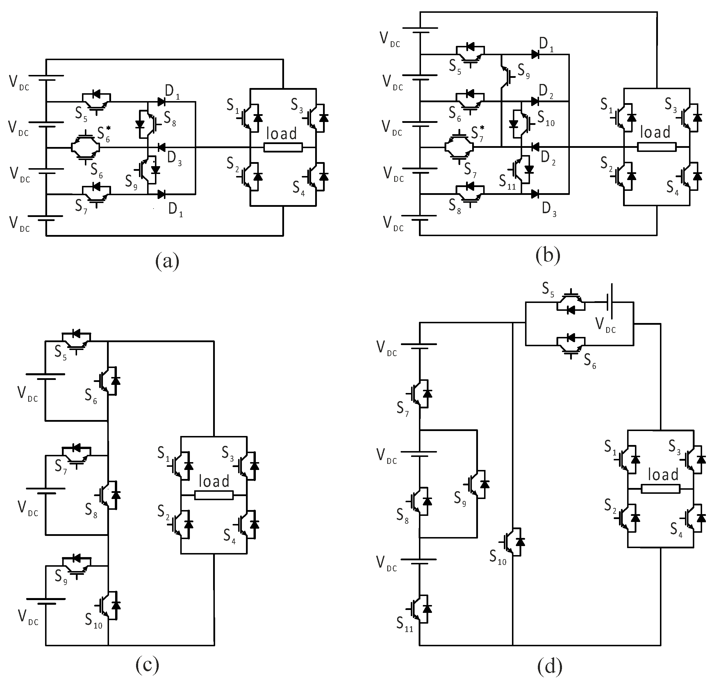
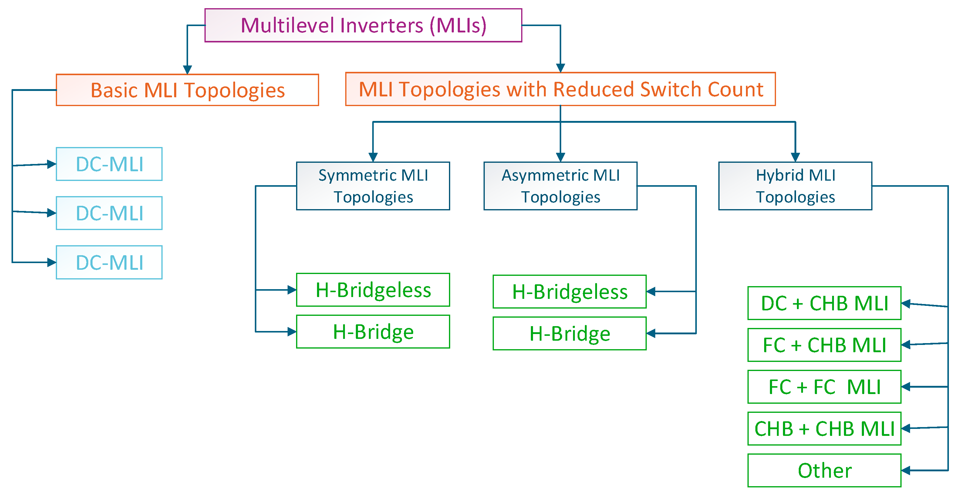
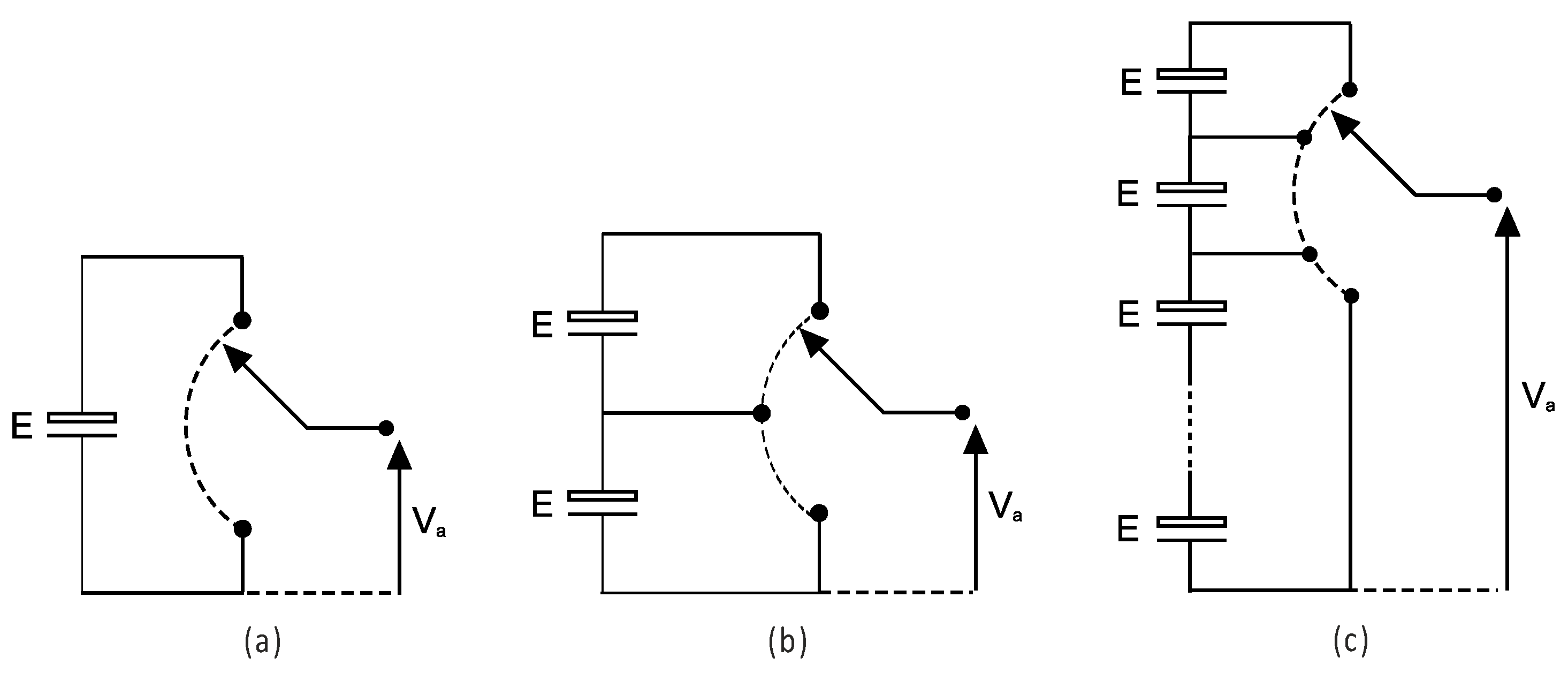
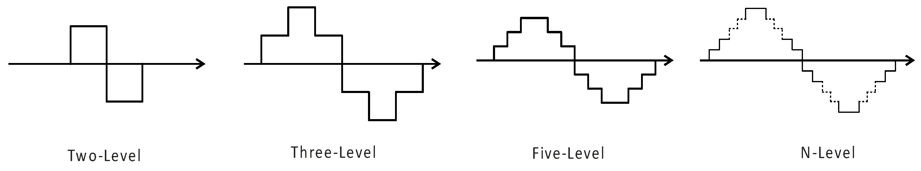
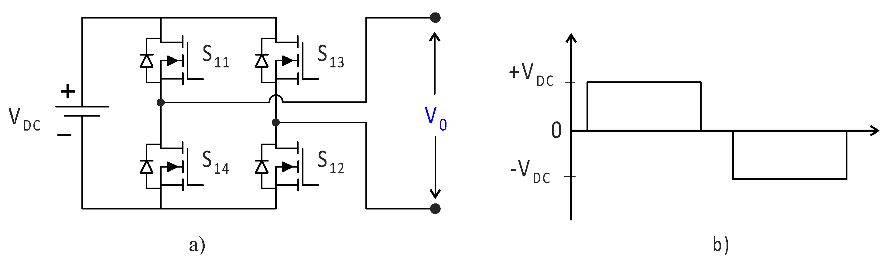
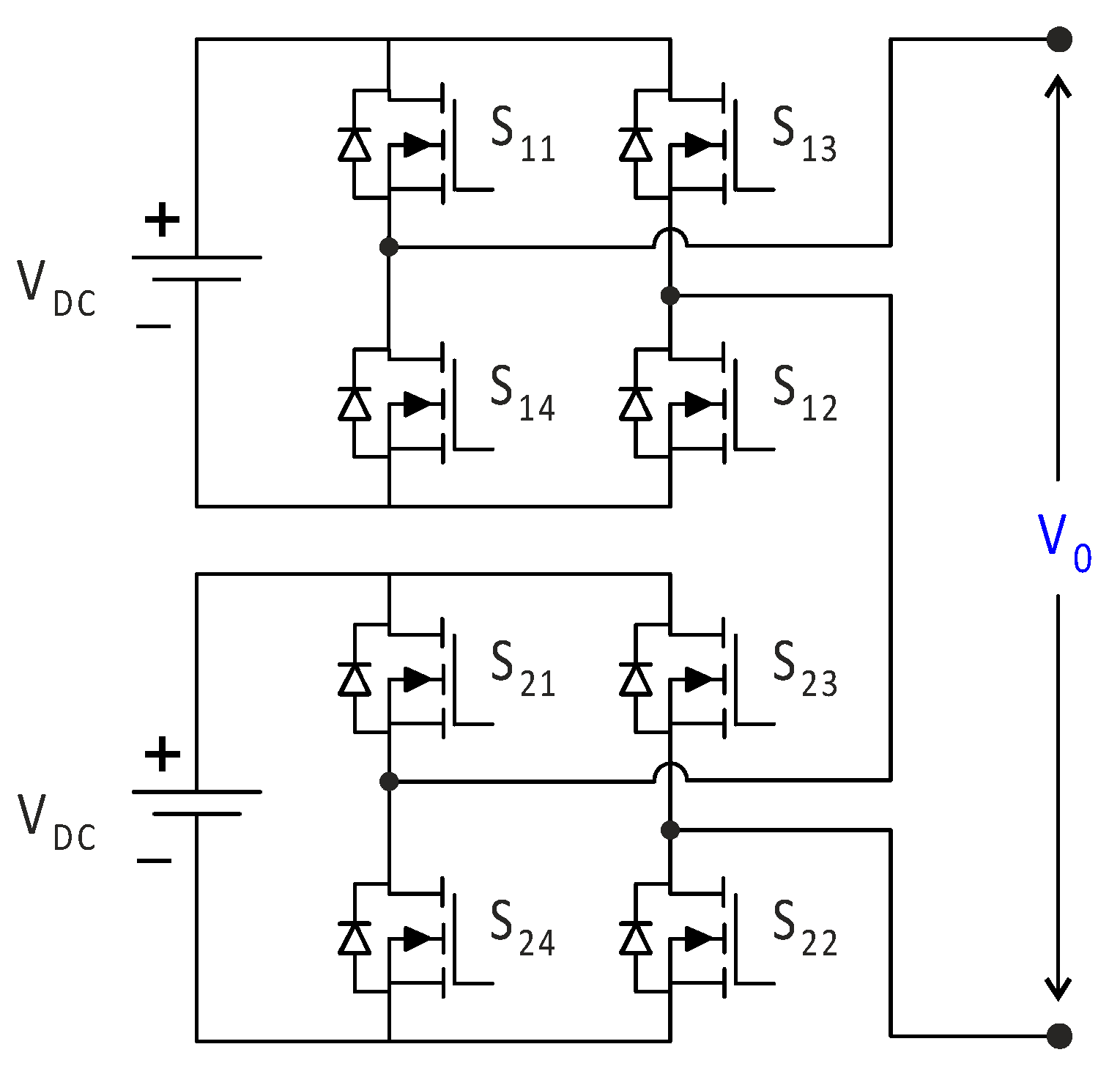

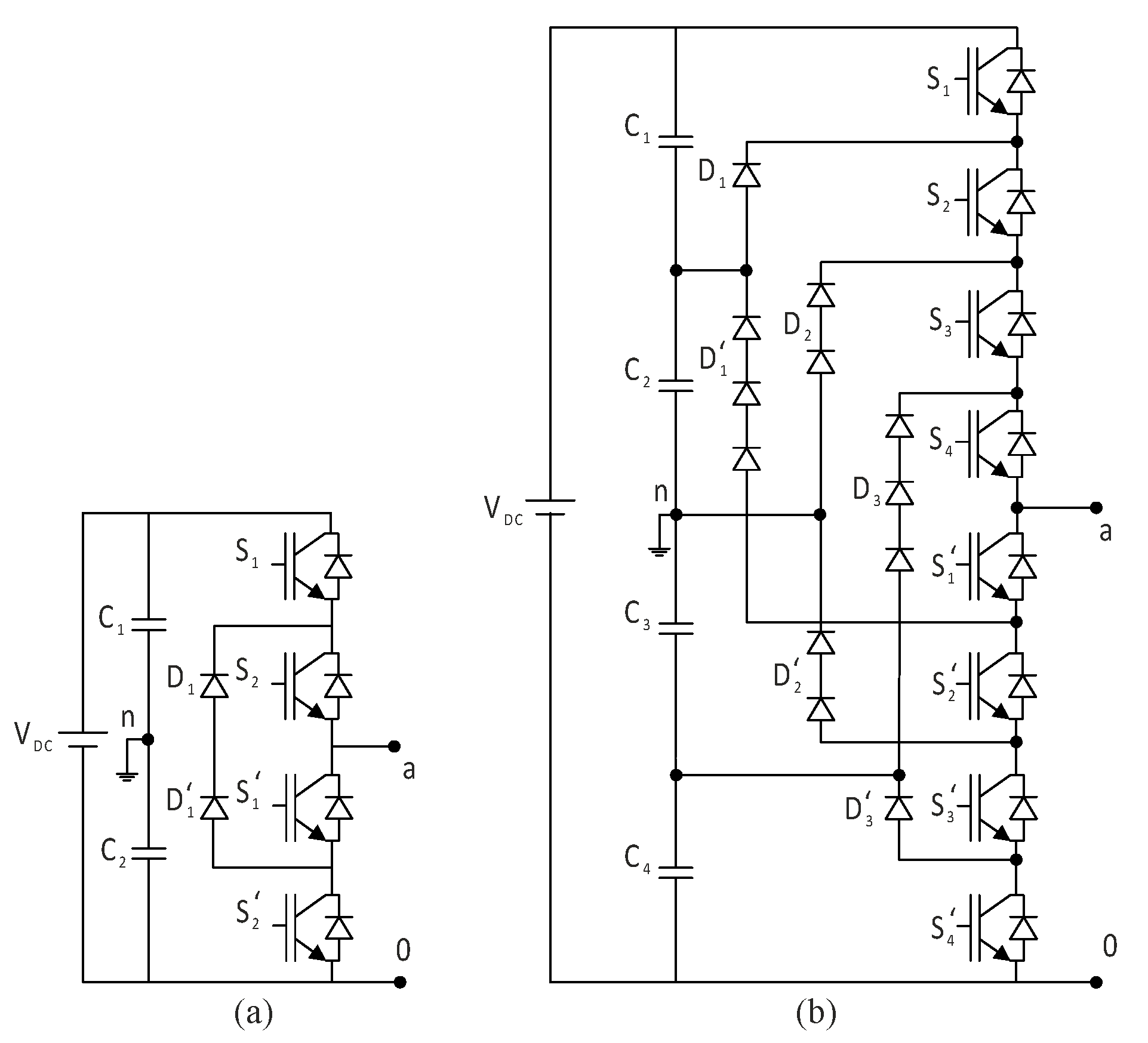
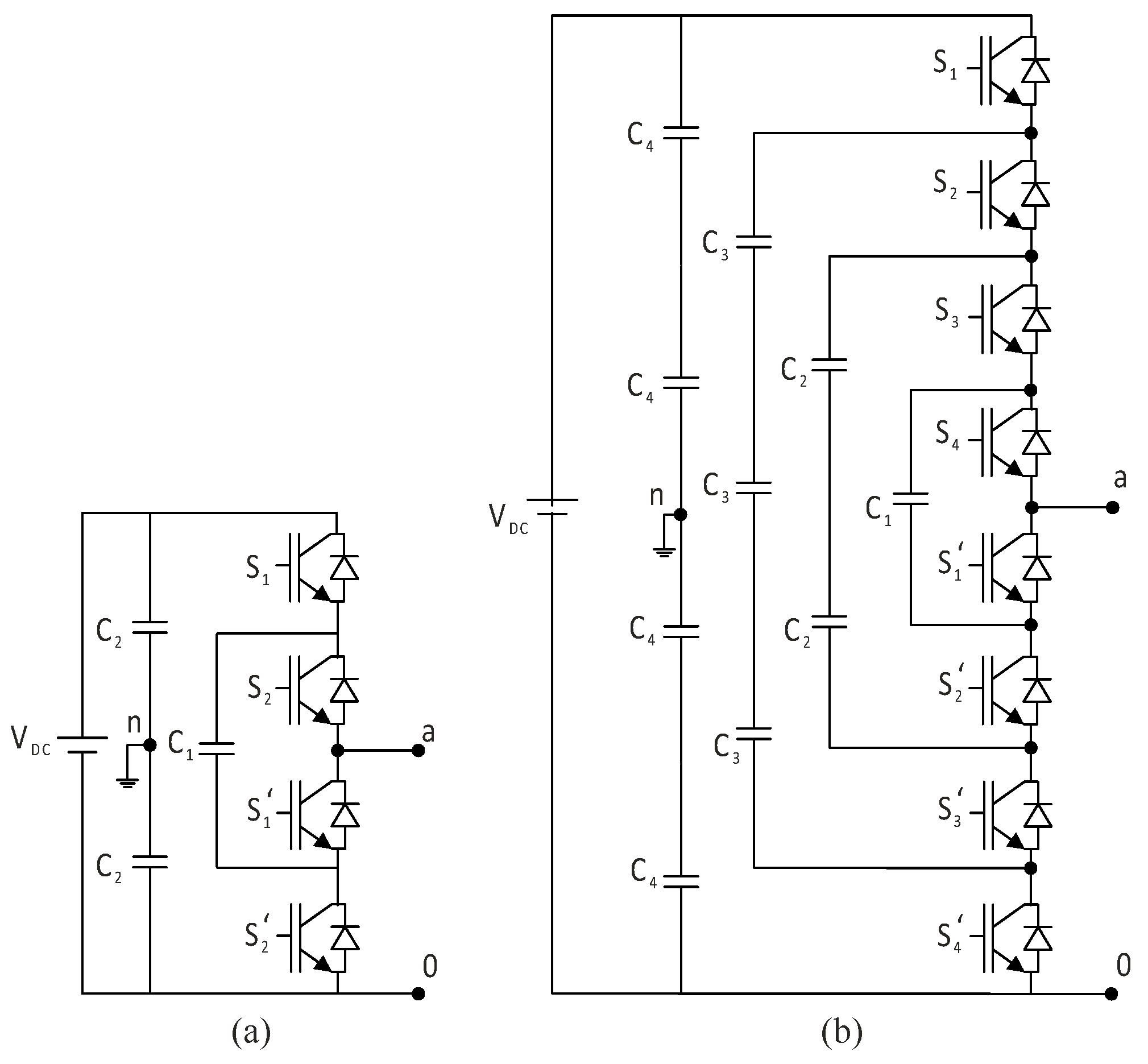
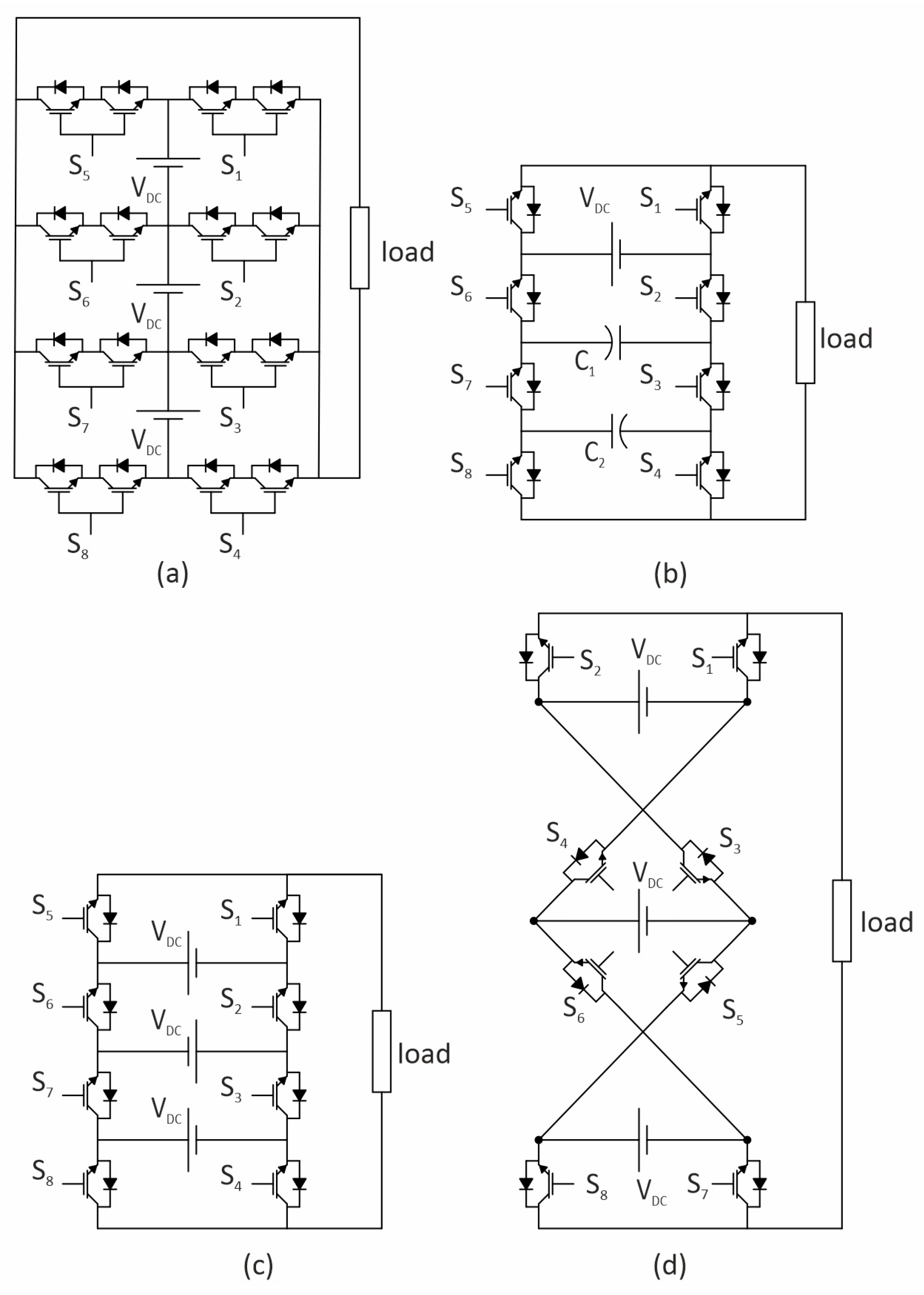
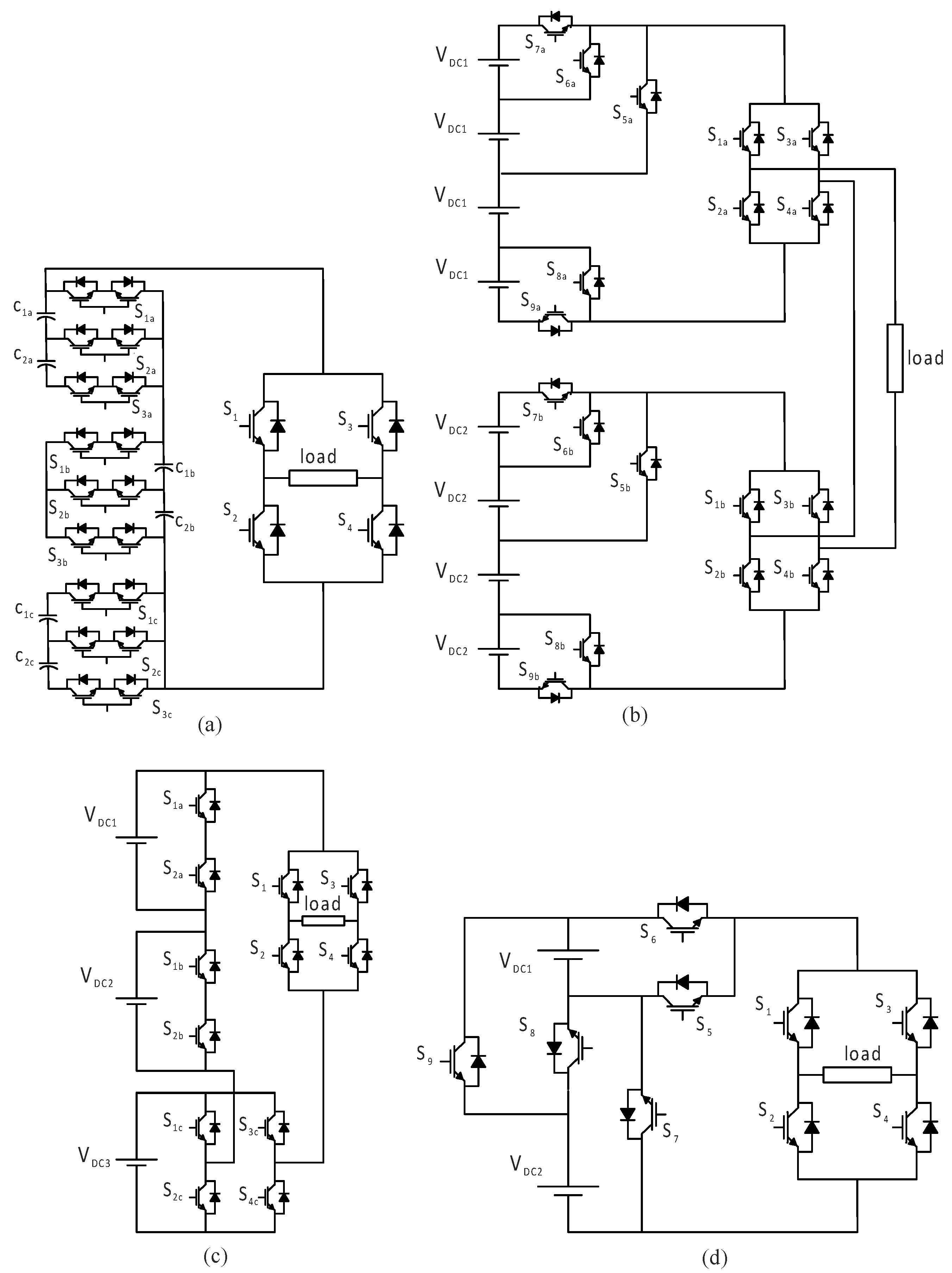

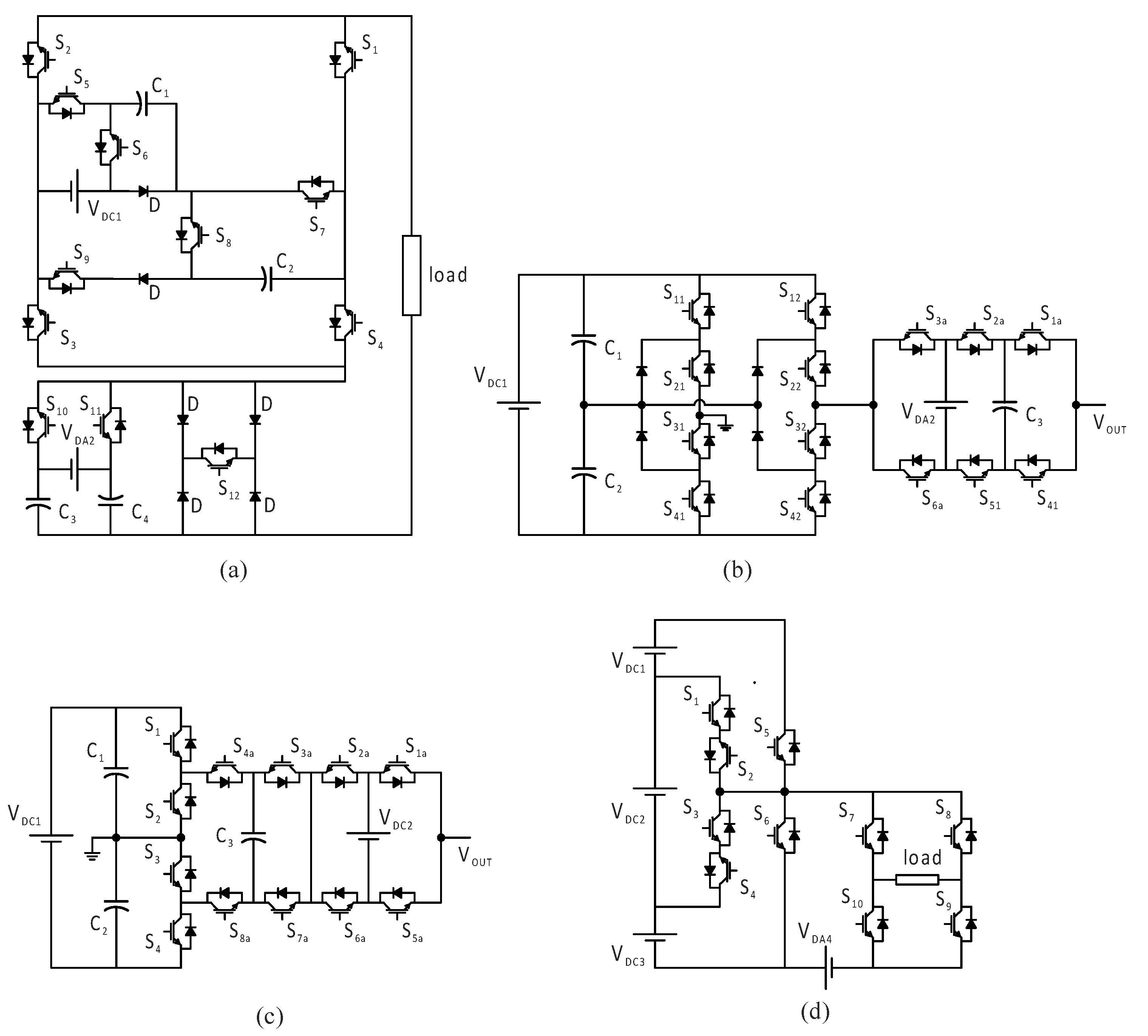
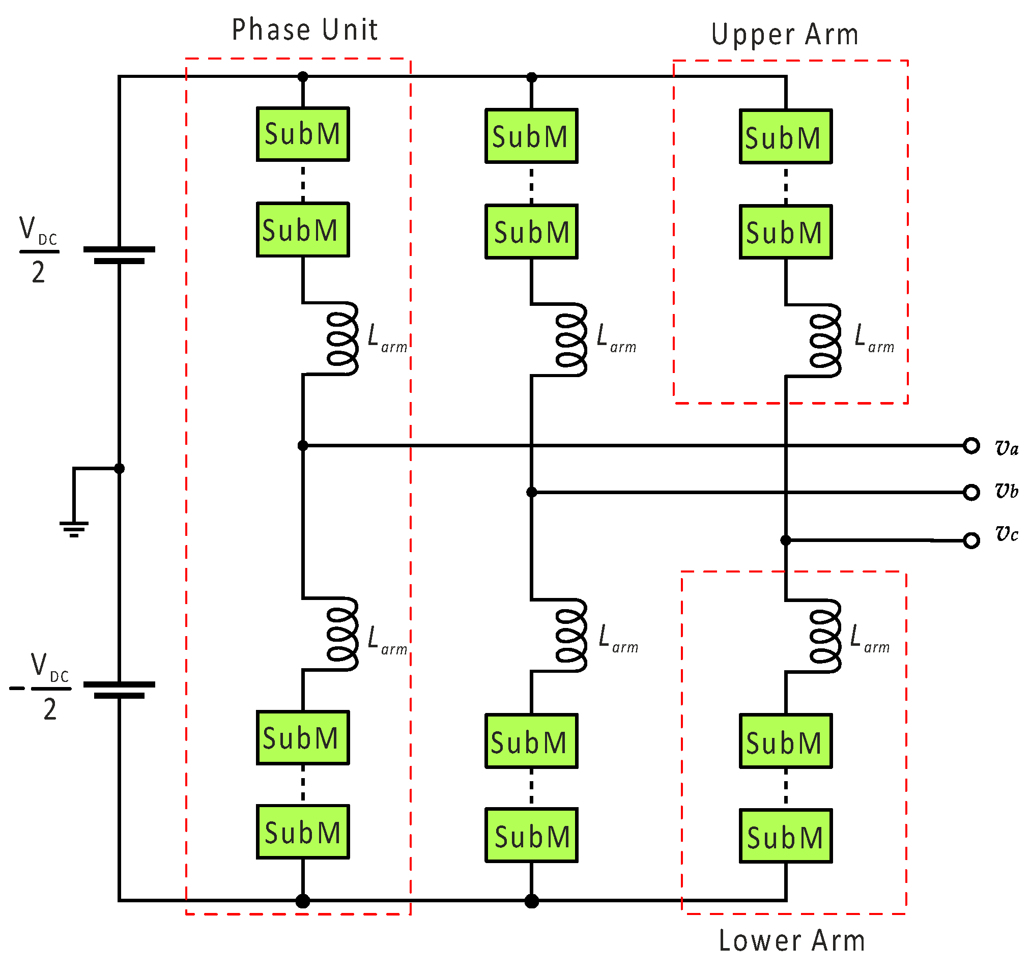
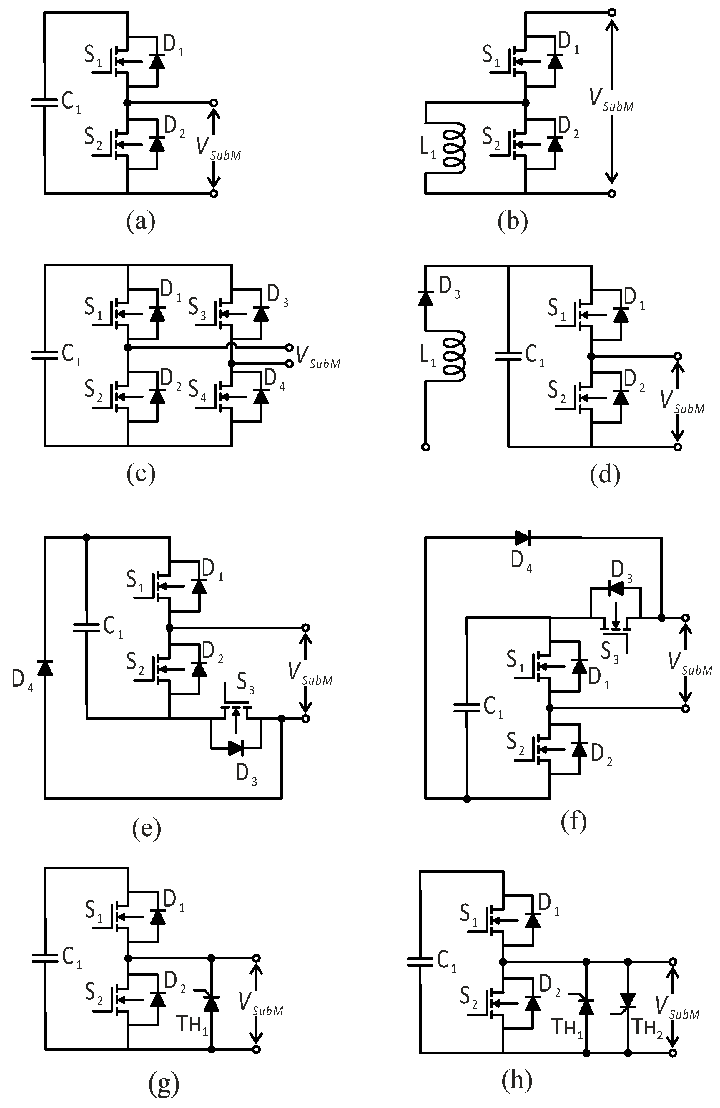
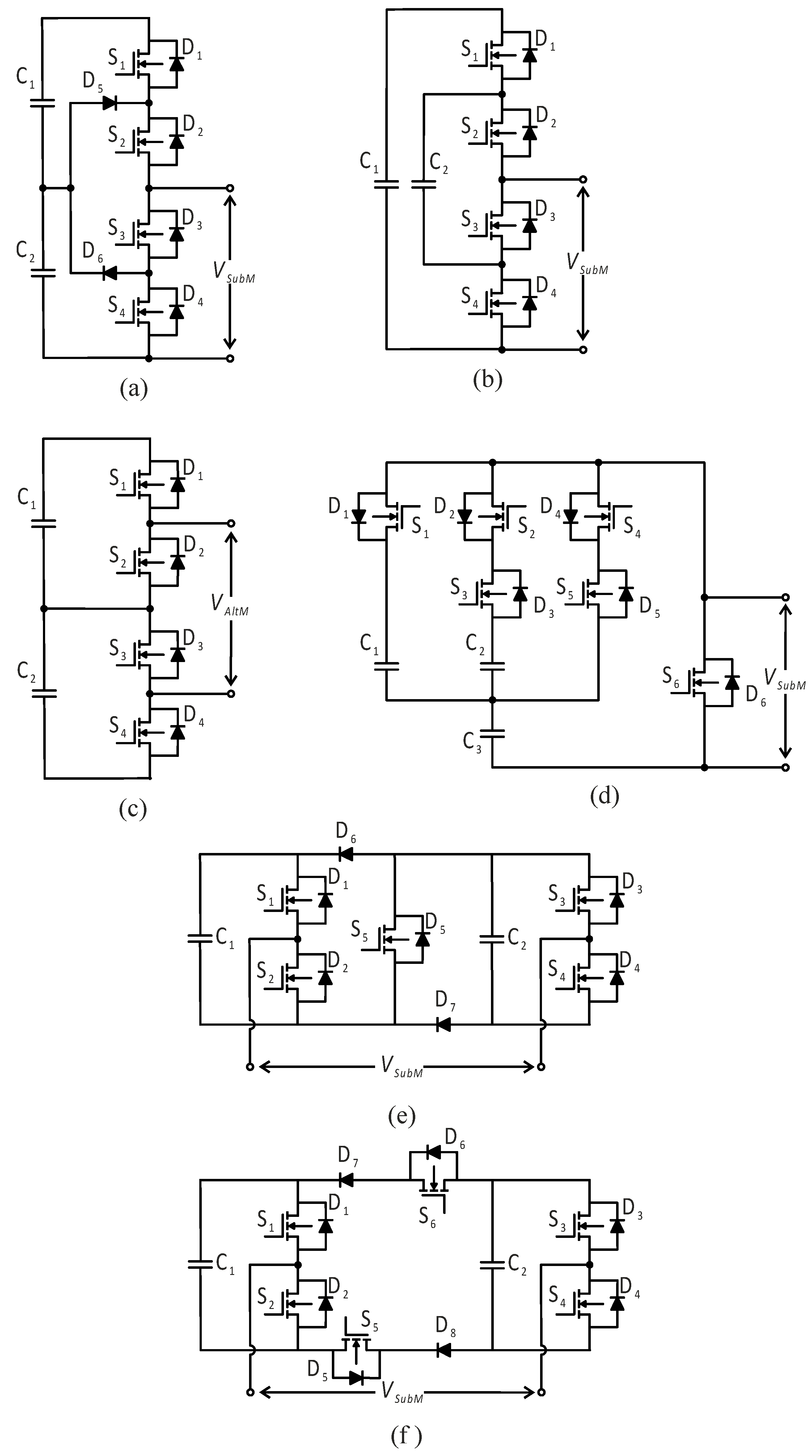

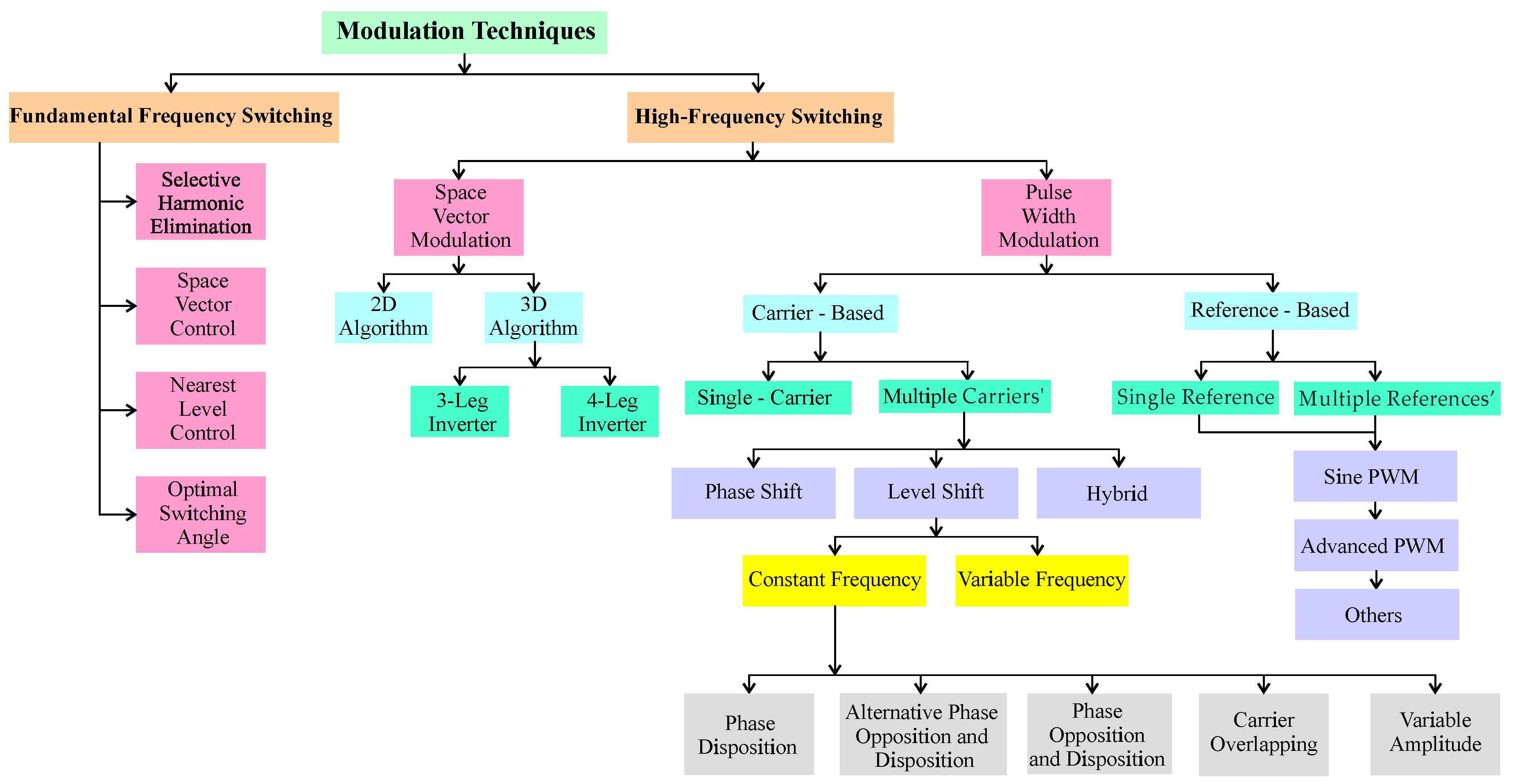
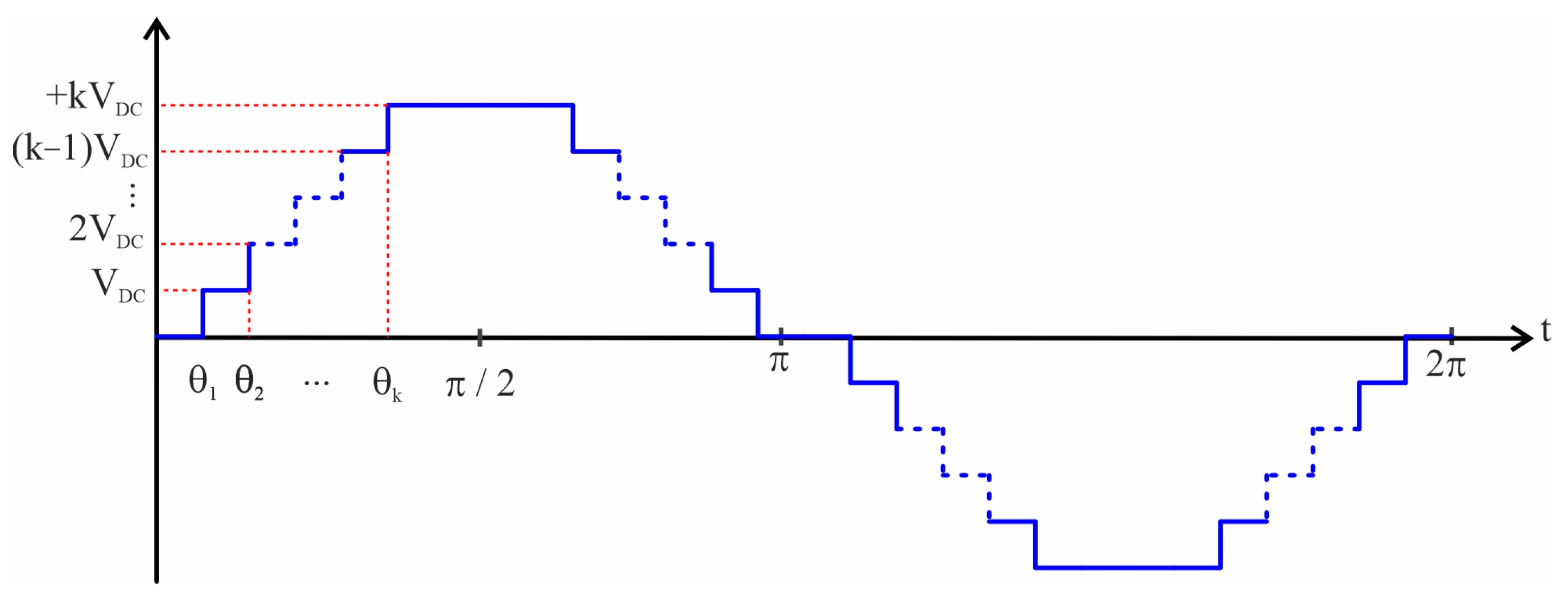
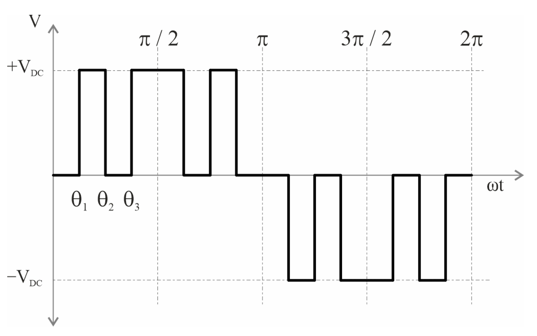
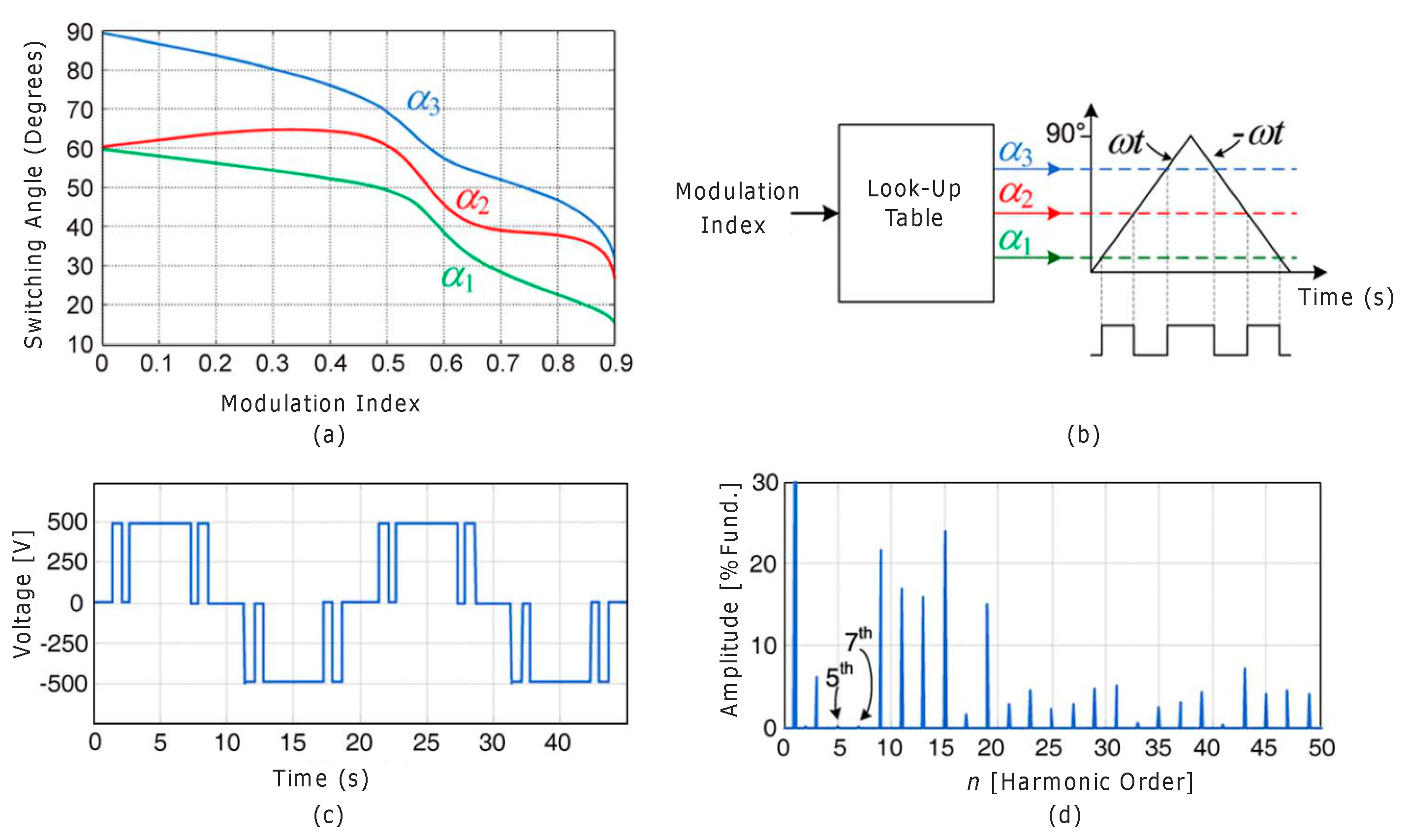
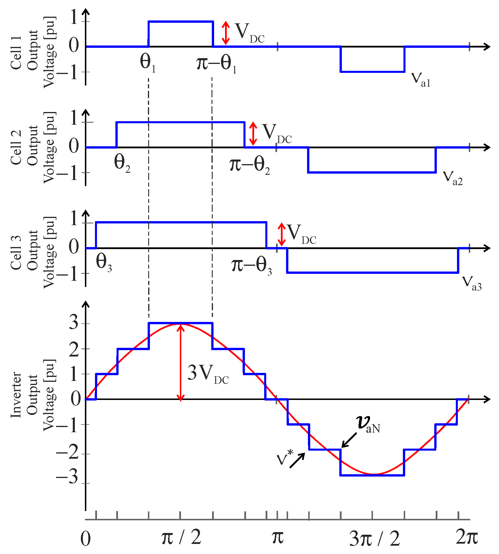
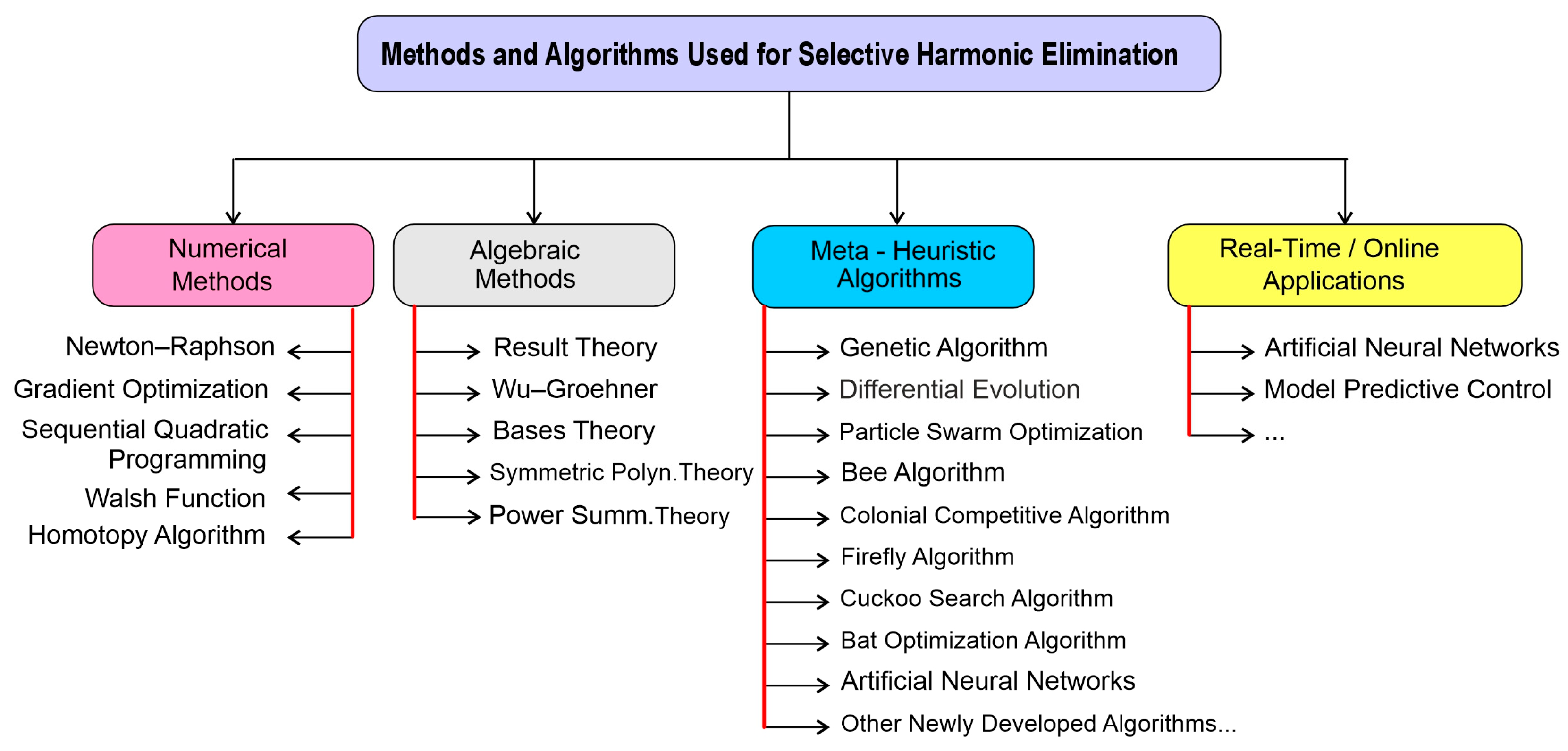
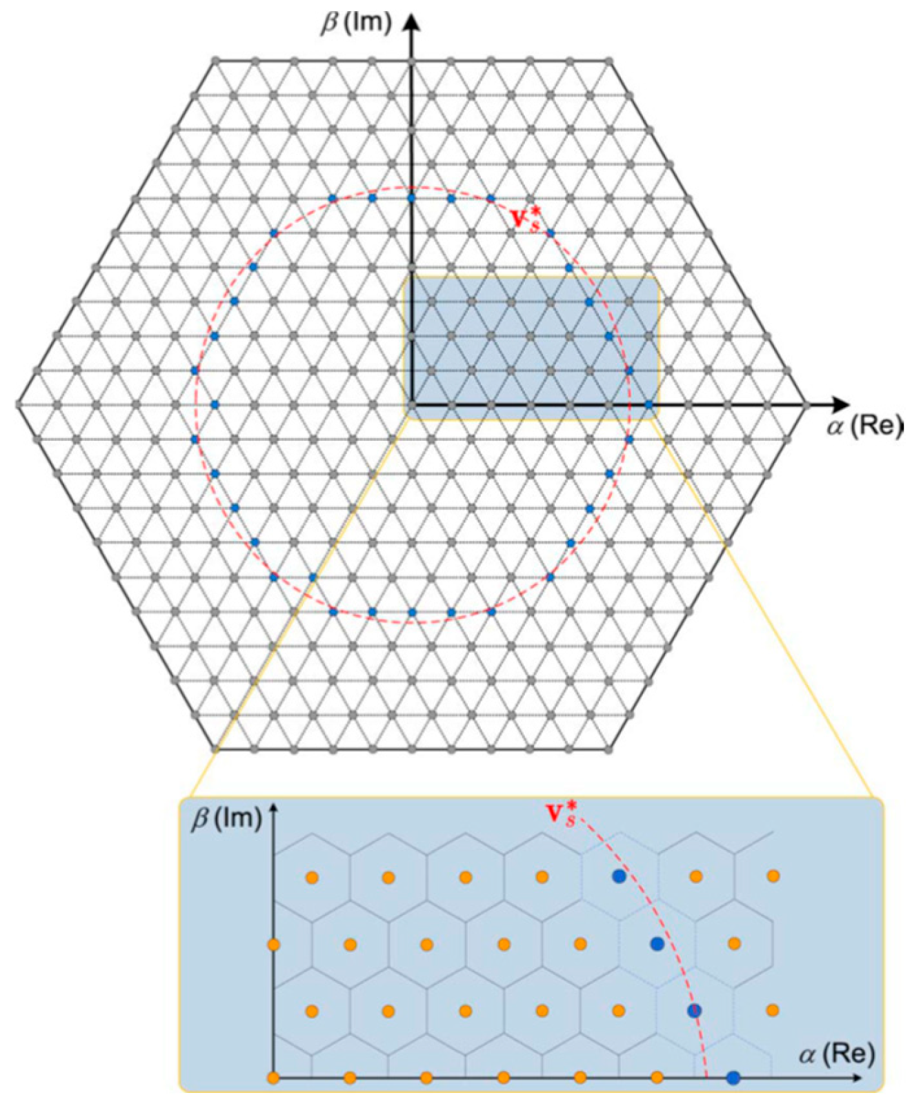
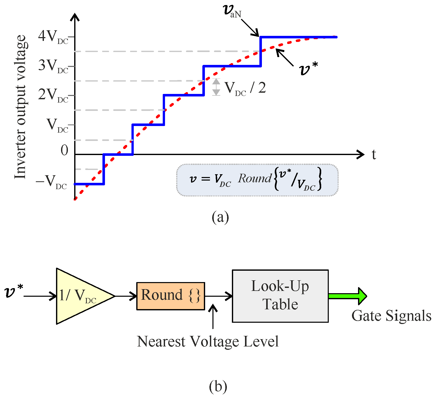
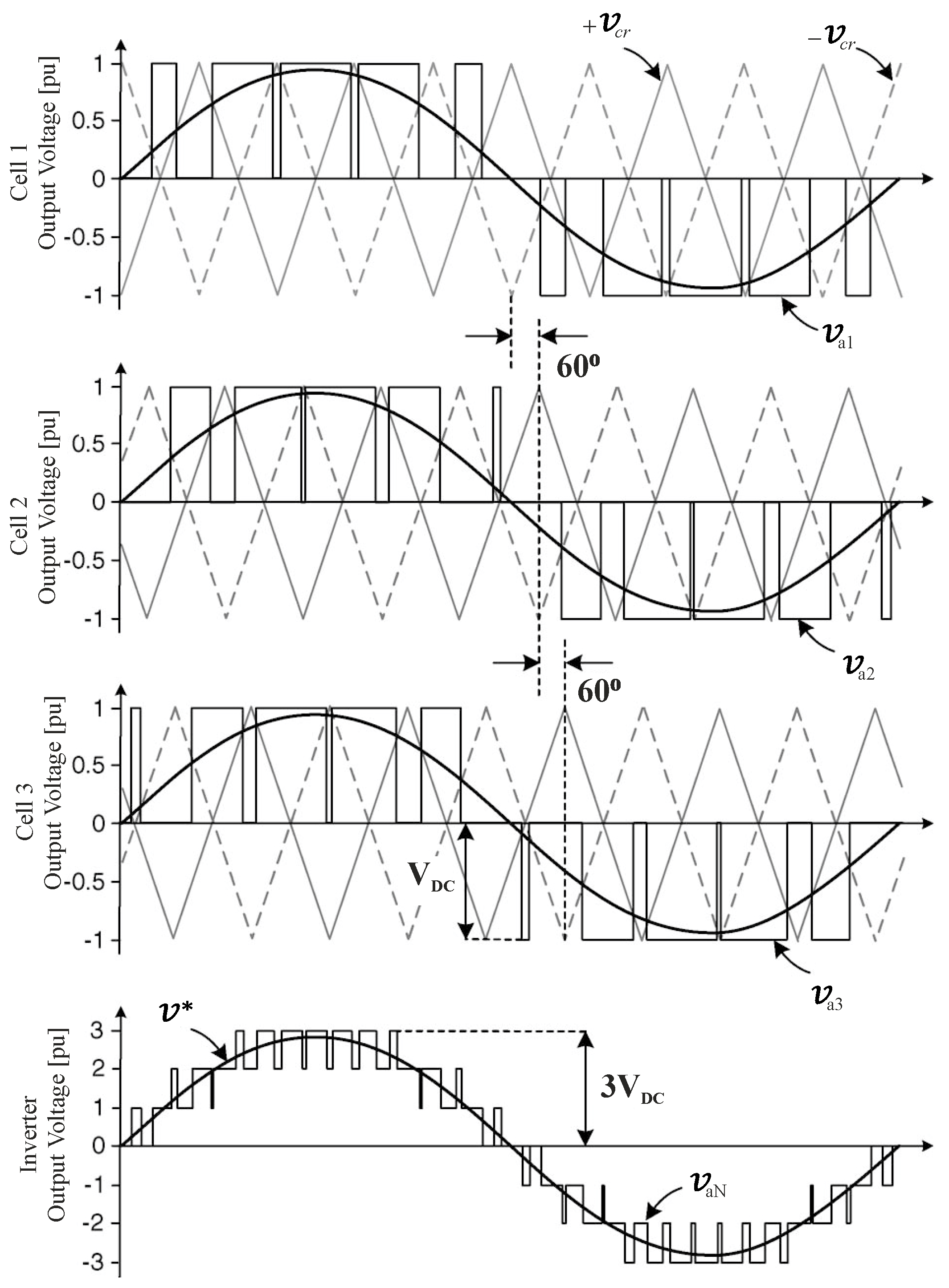
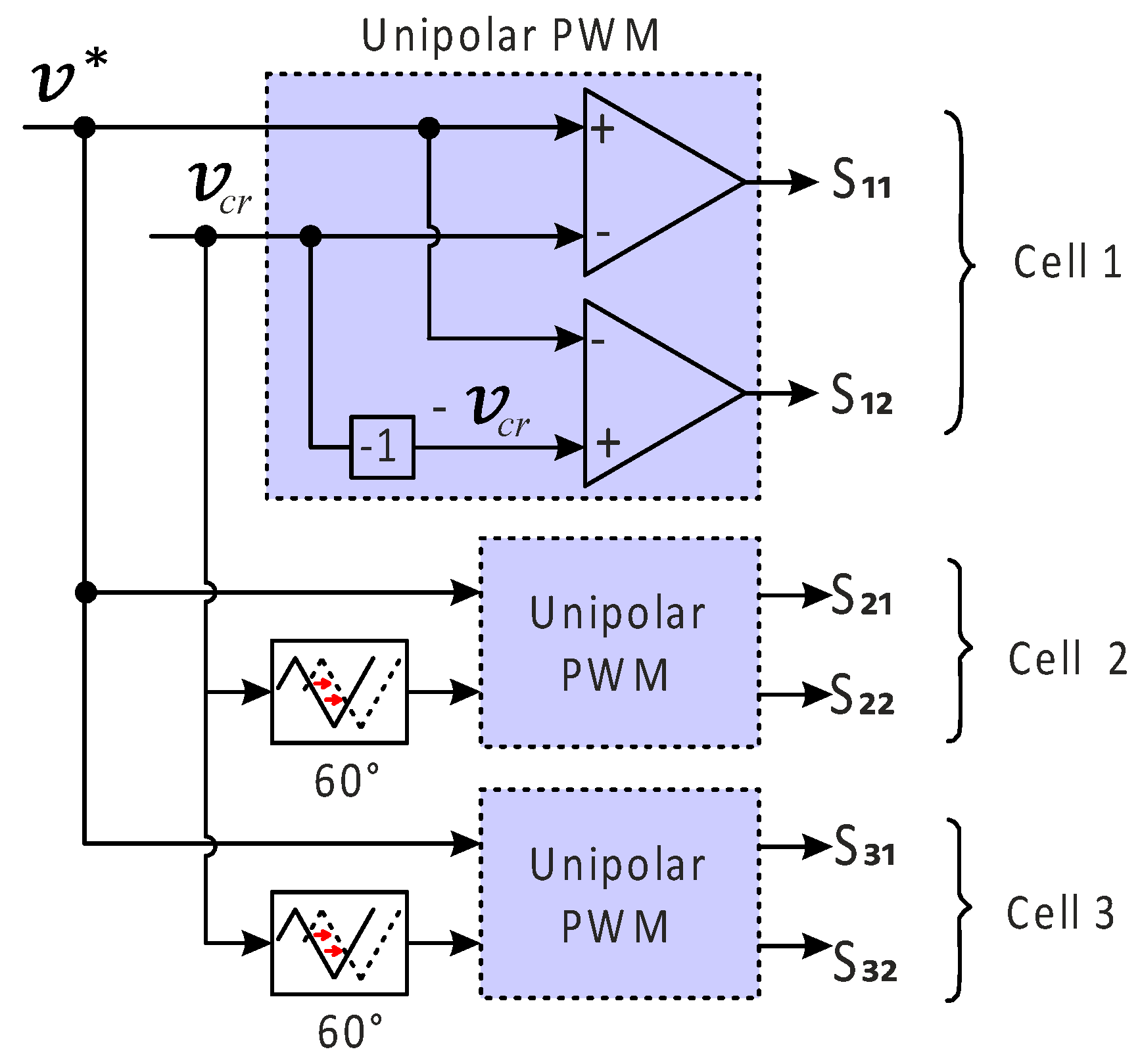
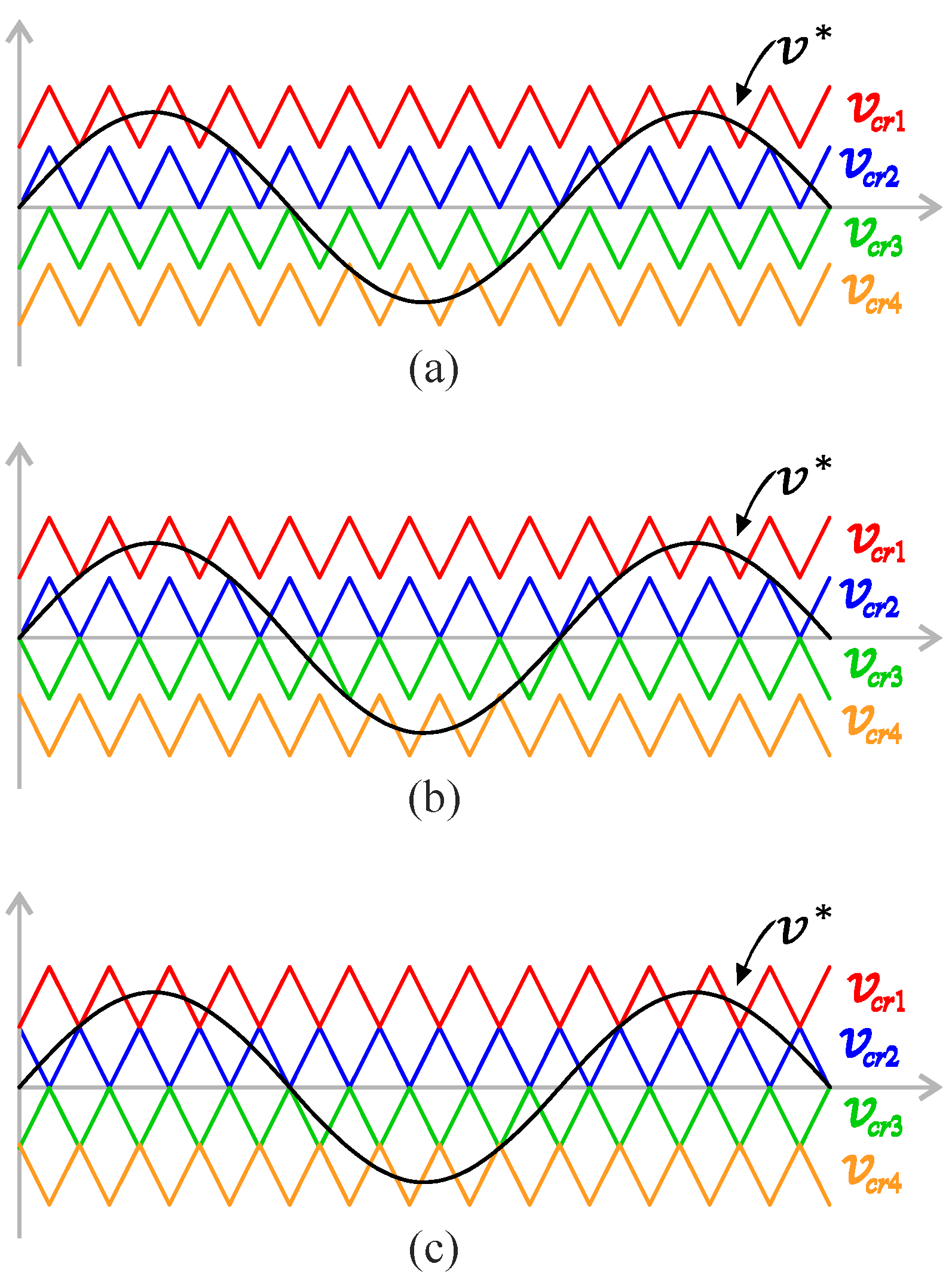
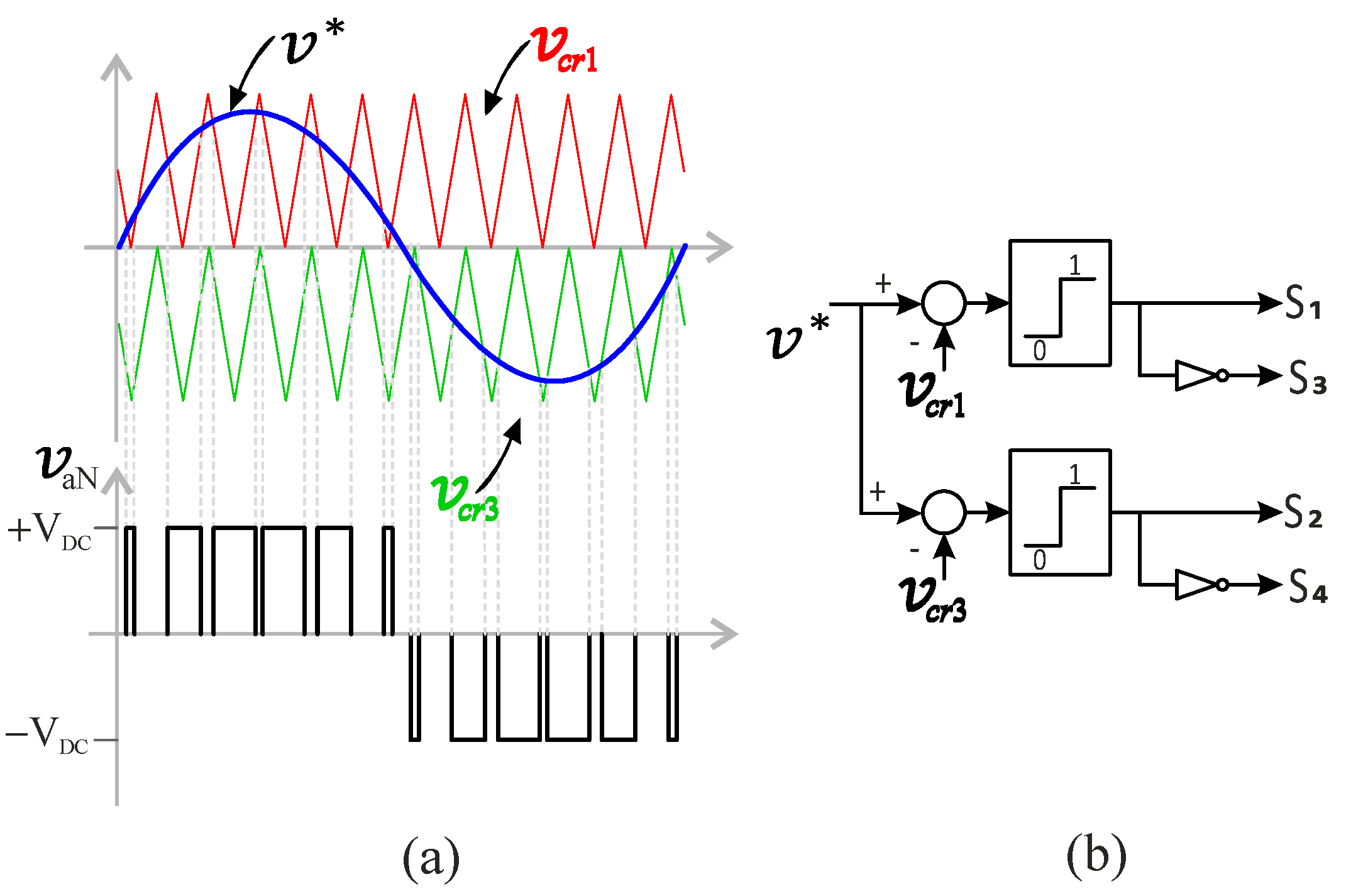
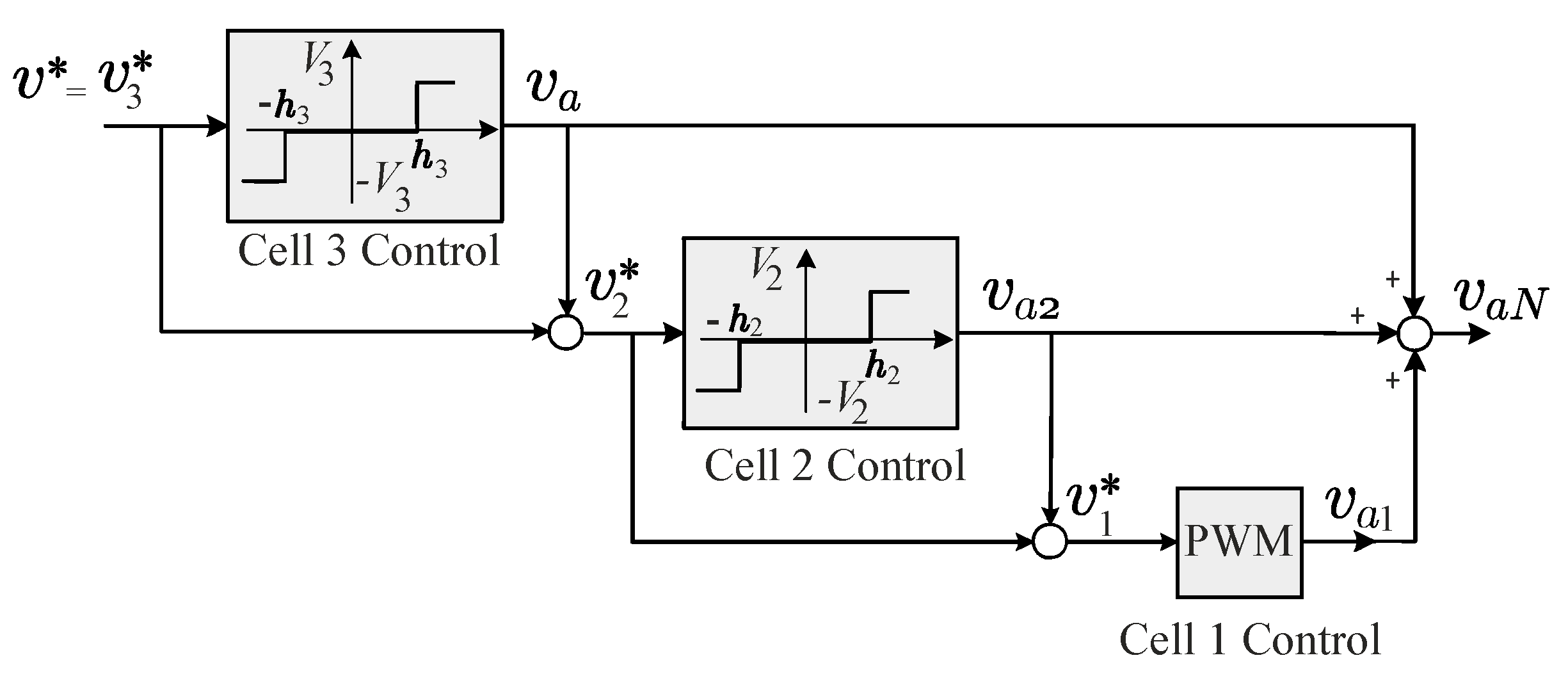

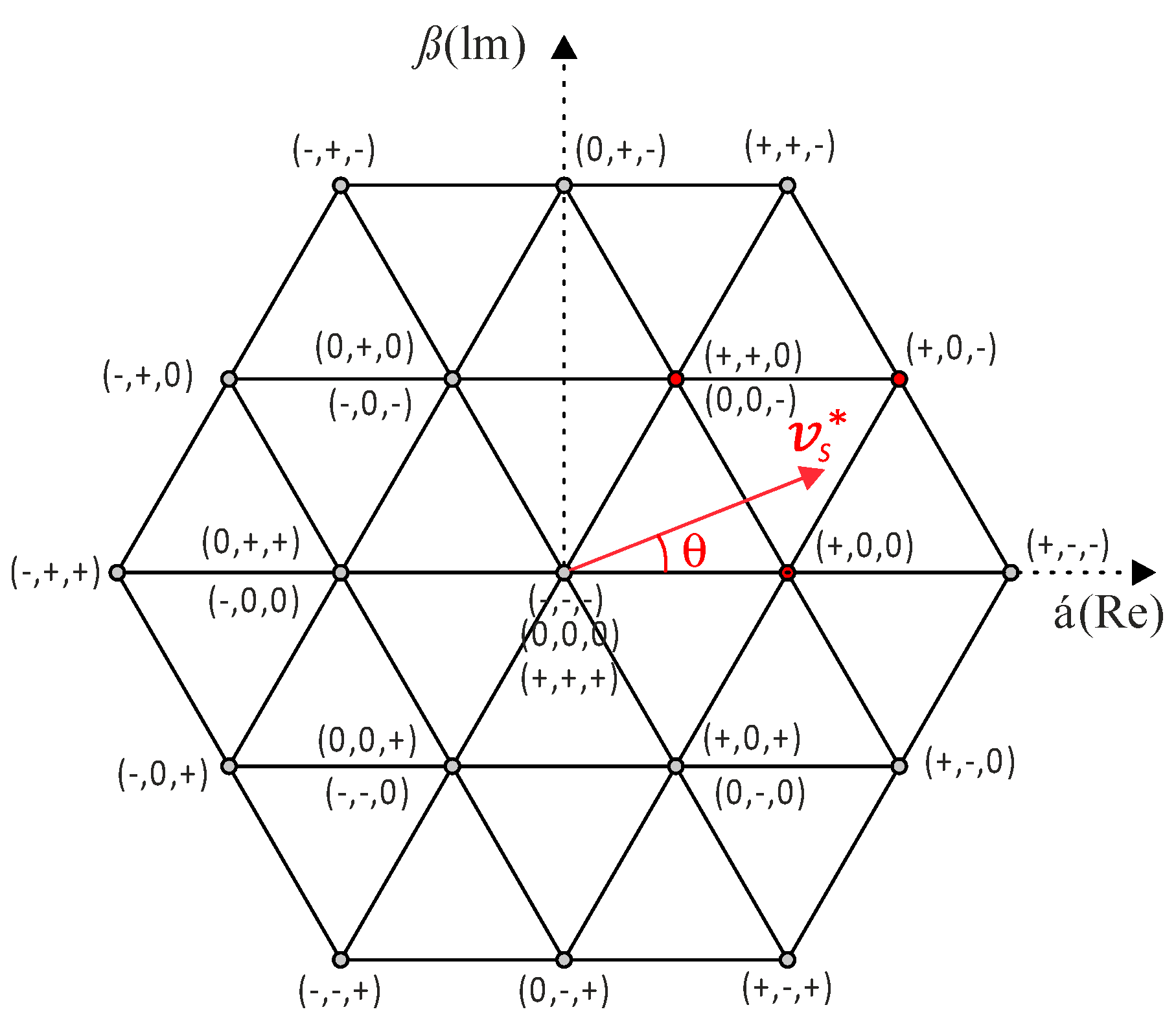
