1. Introduction
The continuous scaling of CMOS technology to nanometer sizes has enabled the development of highly integrated systems for wireless communication, offering benefits such as higher speed, lower power consumption, and reduced area. As a result, CMOS technology is widely adopted for RF applications due to its high-density integration and cost effectiveness. However, this comes with challenges, particularly in maintaining low phase noise and power efficiency. One key issue is the degradation of the on-chip LC tank quality factor, which is typically limited in the GHz range due to thin metal layers and substrate losses [
1]. While advancements in process technology and additional metal layers have gradually improved the quality factor of passive elements [
2], designing high-performance LC voltage-controlled oscillator (VCOs) remains a complex task, especially with the reduced supply voltage that complicates achieving wide linearity and full output swing [
3].
The 5 GHz frequency band is widely used in modern RF applications, including Wi-Fi standards such as 802.11a/n/ac/ax [
4], mid-band 5G networks [
5], and automotive radar systems [
6]. These applications demand low-phase-noise oscillators to ensure reliable communication, reduced signal distortion, and enhanced performance. Furthermore, IoT devices operating in this band benefit from reduced interference and higher data throughput compared to the crowded 2.4 GHz spectrum [
7]. Designing VCOs optimized for such applications is critical to meet the stringent requirements of high-speed data transfer, low power consumption, and robust performance in the presence of noise and interference. This work aims to address these challenges by proposing an efficient optimization methodology tailored to the needs of these 5 GHz applications.
Numerous methodologies for designing LC VCOs have been proposed in the literature. Most studies rely on analytical models to characterize circuit behavior but often ignore parasitic effects, which are only accounted for through simulations. For instance, the
methodology explored in [
8] optimizes LC VCOs across all transistor inversion regions but lacks applicability for varactor characterization. Furthermore, model-based optimization methods combined with genetic algorithms (GAs) have been employed to enhance phase noise and power consumption in RF applications [
9,
10]. Despite their effectiveness, these approaches might miss certain non-idealities captured by electromagnetic simulations, highlighting the need for further validation through Process, Voltage, and Temperature (PVT) and yield analysis.
Recent work in [
11] introduces a wide-tunable, low-voltage LC-VCO using a novel active inductor, achieving impressive performance metrics. However, the absence of optimization algorithms limits further enhancement of phase noise and power consumption, and the use of an active inductor can introduce higher noise and power consumption compared to traditional inductors. Moreover, studies like [
12] employ EDA tools and Evolutionary Algorithms (EAs) for optimal VCO sizing, achieving precise performance trade-offs. Still, their focus on only two LC-VCO topologies may overlook alternative designs that could offer better results, and the computational intensity of such simulations may increase design time and complexity. Similarly, ref. [
13] presents a simulation-based methodology for multi-objective optimization of LC-VCOs, focusing on key metrics like power consumption and phase noise. While validated using 0.13 µm RF CMOS technology, this approach’s reliance on extensive simulations can make it computationally expensive, demanding significant time and resources, especially for more complex RF circuits. In [
14], the authors propose a new multi-objective optimization methodology for designing a complementary cross-coupled LC-VCO, aiming to minimize both phase noise and power consumption. This approach leverages a multi-objective algorithm that enhances exploration and exploitation, theoretically improving oscillator performance. However, the work has several limitations: it lacks validation through circuit simulation, limiting practical applicability, and, despite claiming a multi-objective approach, only a single solution is presented, which undermines the multi-objective framework. Additionally, the VCO modeling uses simplified equations that may not adequately capture the complexities of real-world VCO behavior.
According to recent reviews of metaheuristic optimization in analog circuit design, the vast majority of reported studies rely on population-based approaches, particularly genetic algorithms, evolutionary strategies, and swarm intelligence. Among these, GAs and NSGA-II are by far the most frequently employed for analog and RF circuit sizing, reflecting their maturity and community adoption [
15,
16]. Nonetheless, the same reviews also document an increasing adoption of hybrid schemes (e.g., PSO–DE combinations), surrogate-assisted optimizers (such as surrogate-augmented DE or ESSAB [
17]), and more recent swarm-based innovations (e.g., MSSA, MOBO/D), which offer promising improvements in convergence speed and scalability [
18,
19,
20]. While classical algorithms remain critical as baselines and for comparability across studies, the integration of recent algorithms highlights the research momentum toward more efficient, hybridized, and machine-learning-assisted metaheuristics in analog design [
21,
22].
Recent surveys of metaheuristic-based analog design confirm that these methods remain the most widely adopted tools for circuit optimization due to their ability to handle nonlinear, non-differentiable, and simulation-driven objectives. Evolutionary and swarm intelligence approaches such as GA, PSO, and DE dominate the literature, while multi-objective variants like NSGA-II and SPEA2 remain the most frequently applied to balance conflicting circuit performance metrics. At the same time, newer trends include hybrid [
20] and surrogate-assisted metaheuristics [
18,
19] that aim to reduce the high computational cost of repeated SPICE simulations, as well as physics-inspired and decomposition-based approaches (e.g., MOEA/D, MSSA) that enhance convergence speed and Pareto diversity. Importantly, the recent taxonomy of methods also highlights the growing role of machine learning integration [
17,
21,
22], such as ANN-assisted differential evolution [
16] or surrogate-guided search [
17], for handling high-dimensional analog design tasks. These findings emphasize both the maturity of classical algorithms and the momentum of recent innovations, situating our proposed framework at the intersection of reliability and state-of-the-art advancement.
While differential LC-VCOs inherently benefit from symmetric topologies to ensure balanced outputs and effective common-mode rejection, practical implementations often introduce asymmetries due to layout constraints, parasitic mismatches, or non-uniform biasing. These asymmetries can degrade performance, particularly phase noise and power efficiency; however, when properly characterized, they may also offer optimization flexibility. In this context, this paper explores how model-based metaheuristic optimization can implicitly account for such structural and layout asymmetries while enforcing performance-driven symmetry in key signal paths.
In this work, we propose a model-based optimization approach that leverages the EKV model for accurate characterization of circuit elements combined with metaheuristic algorithms. Our methodology, demonstrated through case studies using 180 nm CMOS technology, effectively minimizes phase noise and power consumption. The accuracy of the optimized LC-VCO designs is validated through detailed simulations, and their robustness is confirmed via yield analysis.
It is important to note that the novelty of this work does not lie in introducing a new optimization algorithm. Instead, it resides in the methodological contribution of embedding symmetry and asymmetry considerations directly into EKV-based analytical modeling of LC-VCOs. By enriching the modeling layer, the proposed approach enables existing metaheuristics—whether classical (e.g., GA, PSO, DE, NSGA-II) or modern (e.g., new, hybrid, surrogate-assisted, or machine-learning-based)—to converge toward physically consistent, verifiable, and practically implementable designs. This modeling innovation ensures that optimization outcomes remain both robust and relevant, even without the development of a new algorithm.
The main motivations of this work can be summarized as follows:
To integrate EKV-based physical models with metaheuristics for verifiable LC-VCO design;
To assess how symmetry and asymmetry influence optimization outcomes;
To compare single- and multi-objective optimization in minimizing phase noise and power;
To validate robustness through yield-oriented Monte Carlo simulations.
The rest of this paper is structured as follows:
Section 2 formulates the optimization problem for LC-VCO design.
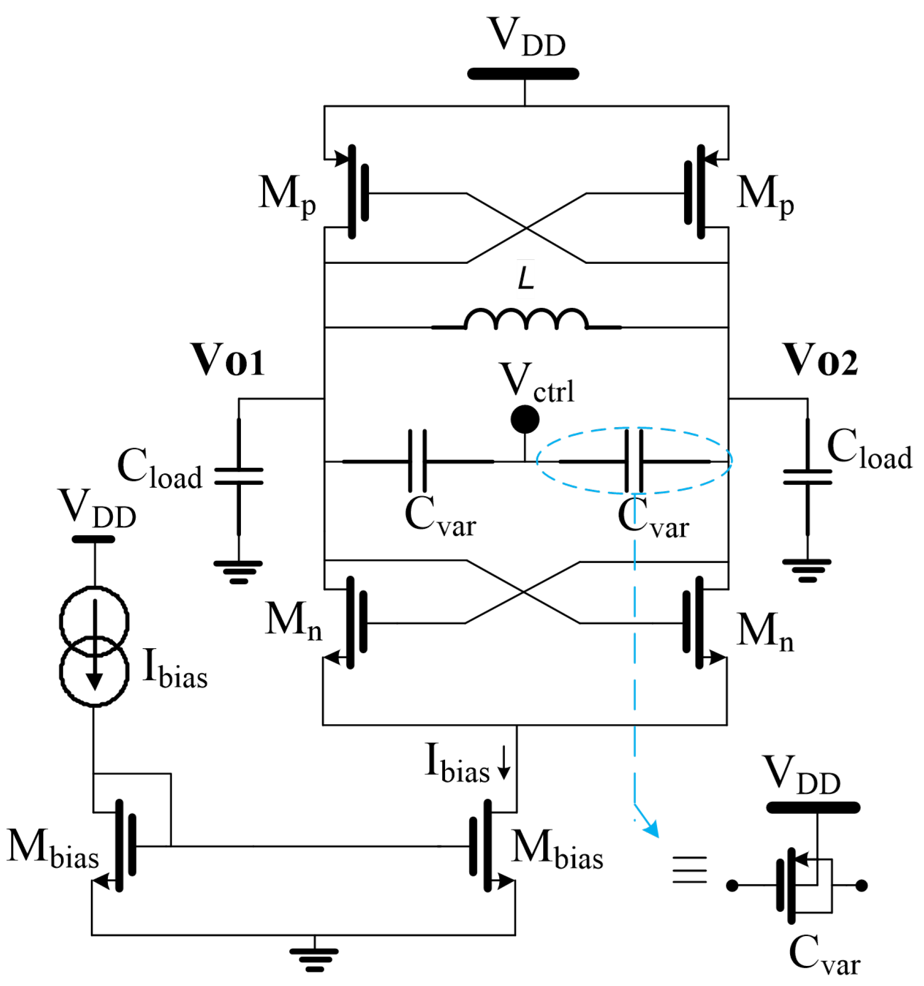
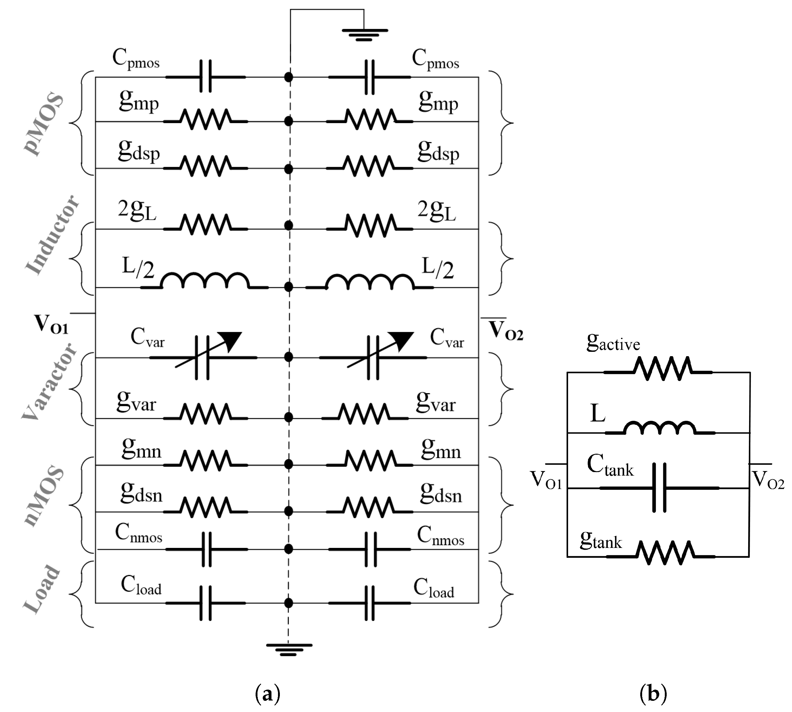
Section 3 presents the LC-VCO topology and modeling, providing the foundational analytical models for the spiral inductor and CMOS varactor as well as performance characterization.
Section 4 discusses the LC-VCO optimization results, with detailed analysis and comparisons. Finally, conclusions are drawn in
Section 5.
2. LC-VCO Optimization Formulation
The circuit optimization problem focuses on determining the optimal set of design parameters that maximize or minimize specific performance metrics of a circuit, while satisfying a set of constraints. In the context of LC-VCO design, the optimization problem seeks to determine the optimal set of design parameters that improve critical performance metrics. The optimization can be formulated as follows:
Here, represents the set of objective functions, which can be a circuit characteristic or combination of characteristics to be optimized. In the case of LC-VCO design, this typically includes phase noise, power consumption, and other metrics such as the tuning range or oscillation frequency.
The vector consists of the d design parameters, where each parameter corresponds to a specific element of the LC-VCO circuit, such as transistor dimensions, inductor and capacitor sizes, or biasing currents. Each design parameter is constrained by lower bounds and upper bounds , ensuring that they remain within feasible ranges based on technology limitations or physical constraints. The set S denotes the design space, encompassing all possible combinations of design parameters within their bounds.
The inequality constraints typically represent physical limitations, such as the maximum allowable power or biasing conditions, while the equality constraints might correspond to specific circuit conditions, such as ensuring that the oscillation frequency of the LC tank matches the desired target frequency.
Constraint handling is implemented using a static penalty approach. Violations of design constraints—such as deviations in oscillation frequency () or exceeding power limits—incur additive penalties proportional to the severity of the violation. This method ensures that infeasible solutions are penalized, guiding the optimization algorithm toward feasible and high-performance LC-VCO designs.
By formulating the problem in this way, the optimization aims to balance multiple objectives, such as reducing phase noise while minimizing power consumption, under the constraints imposed by the LC-VCO design and technology. This problem formulation enables the use of various optimization algorithms to explore the design space and find the best solution and/or trade-off between competing performance goals.
4. Optimization Results and Discussions
This section outlines the optimization procedure for the LC-VCO circuit, addressing two experimental setups:
(i) Single-objective optimization, where the goal is to minimize phase noise to enhance signal purity. Here, the outcome is a single optimal solution that achieves the minimum phase noise while satisfying imposed constraints.
(ii) Multi-objective optimization, which simultaneously minimizes both phase noise and power consumption,
, to achieve a balanced trade-off between performance and energy efficiency. In this case, minimizing
F in Equation (
1) generates a set of Pareto-optimal solutions, forming the Pareto set, representing trade-offs between phase noise and power consumption. The mapping of the Pareto set into the objective space results in the Pareto Front.
In both setups, the circuit optimization is formulated as a constrained optimization task, as described in Equation (
1). A key constraint in the VCO design optimization is ensuring that the output signal frequency closely matches the desired target frequency,
. To achieve this, the constraint
is imposed, representing the allowable deviation of the actual output frequency from the target frequency
. This ensures that
is constrained to be within
, allowing a small relaxation margin in line with design requirements. Here, the target oscillation frequency of the LC-VCO is
= 5 GHz, while
denotes the actual oscillation frequency of the optimized LC-VCO.
For the single-objective optimization experiments, we used several metaheuristic algorithms, including Particle Swarm Optimization (PSO) [
32], Artificial Bee Colony (ABC) [
33], Ant Colony Optimization (ACO) [
34], Butterfly Optimization Algorithm (BOA) [
35], Differential Evolution (DE) [
36], Equilibrium Optimizer (EO) [
37], Firefly Algorithm (FA) [
38], Genetic Algorithm (GA) [
39], Simulated Annealing (SA) [
40], and Whale Optimization Algorithm (WOA) [
41]. For the multi-objective optimization experiments, we employed multi-objective metaheuristics, specifically, Non-dominated Sorting Genetic Algorithm II (NSGA-II) [
42], Multi-Objective Particle Swarm Optimization (MOPSO) [
43], Strength Pareto Evolutionary Algorithm 2(SPEA2) [
44], Multi-Objective Evolutionary Algorithm Based on Decomposition (MOEA/D) [
42], Multi-Objective Optimization Based on Decomposition (MOBO/D) [
45], and Multi-objective Salp Swarm Algorithm (MSSA) [
46]. All experiments and algorithms were implemented in
Matlab.
The experiments were conducted on a computer equipped with an Intel Corporation® CoreTM i7-7820HQ CPU @ 2.90 GHz (8 cores) and 16 GB of RAM. Each algorithm was run 100 times for all experiments to reduce the random effects inherent in non-deterministic algorithms. The performance of the algorithms was evaluated and compared based on the average results across these 50 runs, providing a robust measure of algorithmic effectiveness and consistency.
4.1. Experiment 1: Minimizing Phase Noise
In this first experiment, the sizing process is formulated to ensure that the phase noise is minimized while satisfying the required design constraints given in
Table 1. This approach emphasizes achieving the best possible phase noise performance without considering the optimization of other factors such as power consumption.
In this single-objective optimization experiment, we consider two optimization scenarios:
In the first scenario, the varactor and spiral inductor are optimized separately, and their optimal values are then used as fixed parameters in the subsequent LC-VCO optimization.
In the second scenario, the varactor and spiral inductor are treated as optimization variables directly integrated into the LC-VCO optimization process.
4.1.1. Scenario 1: Size Components First, Then Optimize
As mentioned before, in this scenario, we first optimize the spiral inductor and varactor independently. These optimized values are then used as fixed parameters in the LC-VCO optimization, allowing for targeted improvement of the circuit’s overall performance.
- (A)
Spiral inductor sizing
The objective is to maximize the quality factor of the spiral inductor,
, as defined in Equation (
13). This optimization must be achieved while maintaining a fixed inductance of
at the operating frequency
and satisfying the area constraint imposed by the outer diameter
.
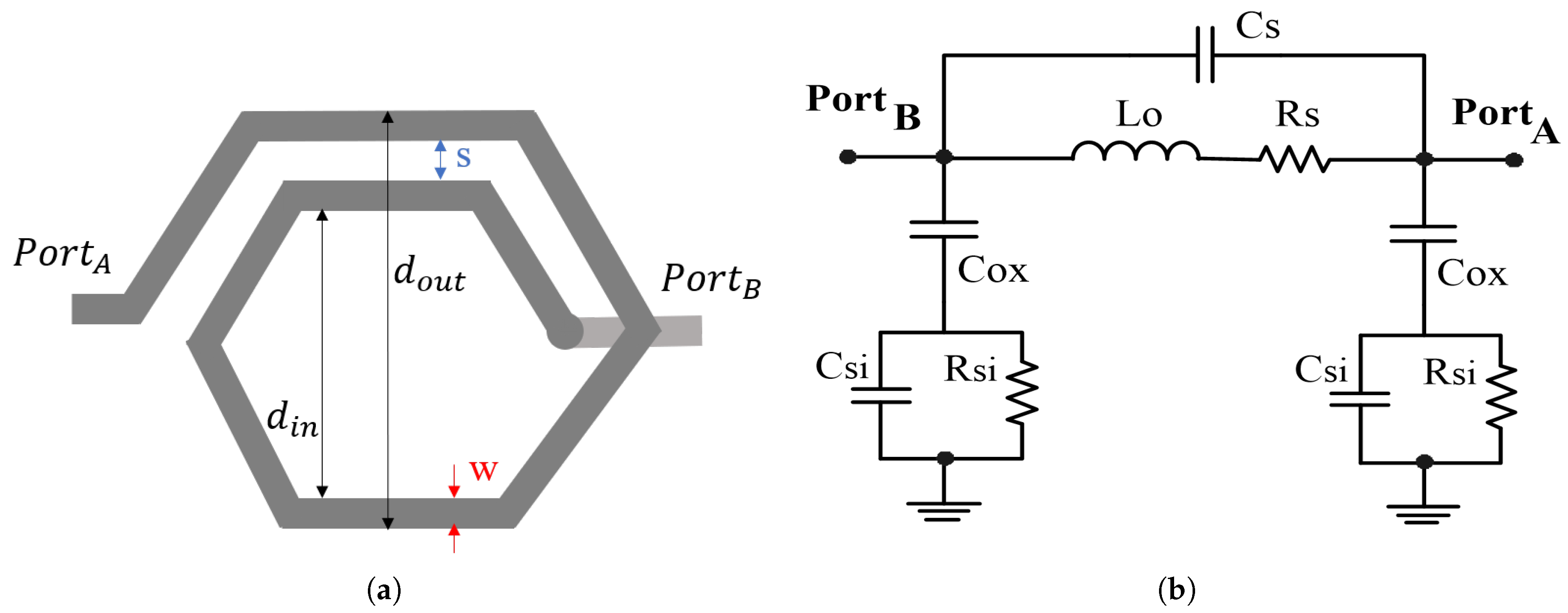
We consider a hexagonal planar spiral inductor topology, as modeled in
Section 3.3. The design variables include the track width (
w), the number of turns (
n), and the internal diameter (
). These variables are constrained within the following ranges:
,
, and
. The spacing between turns is fixed at
, as no improvement is expected from larger spacing.
Table 2 presents a statistical performance comparison of algorithms for spiral inductor sizing, where all methods successfully produced feasible designs in every run. Among the algorithms, PSO, DE, EO, FA, SA, and WOA consistently achieved the best solution (13.0902) with zero variability, demonstrating exceptional efficiency and reliability. WOA is particularly distinguished for its fastest convergence time (10.05 s), closely followed by EO (12.01 s), both excelling in solution quality and speed. ABC also performed well, achieving a good mean solution (13.0448) with low variability (0.0589); however, its convergence time (31.68 s) was slower, but still faster than DE (37.34 s) and FA (42.24 s).
In contrast, BOA shows high variability and gives one of the worst solutions (11.3439), highlighting its reduced reliability. Finally, GA had the worst performance (3.6837), with the lowest mean solution (11.4619), significant variability, and the slowest convergence time (261.47 s), making it less efficient than all other methods in this experiment.
- (B)
CMOS varactor sizing
Here, the objective is to maximize the quality factor of the CMOS varactor,
, as defined in Equation (19), leveraging the EKV MOS model equations described in
Section 3.4. This optimization is carried out at the operating frequency
. The design variables for the varactor include the MOS channel width (
), length (
), and the number of fingers (
). Their respective ranges are
,
, and
.
Table 3 compares the statistical performance of algorithms for varactor sizing, showing their success rates, optimization results, and convergence times. All algorithms achieved feasible designs in every run, except for the BOA algorithm, which had a success rate of 69%, and the GA algorithm, which had a success rate of 82%. PSO, ACO, DE, EO, FA, SA, and WOA consistently found the best solution (10.8066) with no variability, highlighting their reliability. Among these, WOA was the fastest (11.53 s), followed by EO (13.19 s) and SA (17.48 s). DE (39.10 s) and FA (45.97 s) were slower but still efficient. The ABC algorithm, while performing well with a slightly lower mean (10.6777) and minor variability (0.1989), did not achieve the best solution. In contrast, BOA had significant variability, with a mean of 6.3054 and a worst-case value of 4.7841, making it less reliable, despite its best-case solution (10.8047). GA, although it had a competitive best solution (10.4463), showed extreme variability (2.7230) and was the slowest (181.62 s), indicating inefficiency. Overall, WOA excelled in speed and reliability, with EO and SA also providing robust and efficient performance, while BOA and GA were less suited for this task.
- (C)
LC-VCO sizing based on sized LC tank parameters
The objective in this experiment is to minimize phase noise in the cross-coupled CMOS LC-VCO, optimized in
CMOS technology, using the previously optimized spiral inductor and varactor, fulfilling the constraints listed in
Table 1. Some of these constraints are already met through the prior optimization of the LC tank components. The optimized component sizes for the varactor are
,
, and
; and for the spiral inductor are
,
, and
.
In this setup, the design variables for the LC-VCO are , , , , , , and . To simplify the design, all transistors of the same channel type are assigned the same geometric sizes, with and . This simplification reduces the set of design variables to three key parameters: , , and . The ranges for these variables are defined as follows: , , and .
Table 4 compares the performance of various algorithms for LC-VCO sizing, showing that most algorithms, with the exception of ACO and GA, consistently achieved identical objective function values with a 100% success rate and zero standard deviation, demonstrating high reliability in phase noise minimization. ACO, with a 100% success rate and a standard deviation of 0.0016, performed similarly to the other algorithms, while GA achieved a success rate of 84% but showed a higher variability (standard deviation of 2.47). Notably, PSO, ABC, ACO, BOA, DE, EO, FA, SA, and WOA showed consistent results, with WOA being the fastest (17.57 s), followed by SA (22.66 s). GA, while efficient in some runs, exhibited a lower mean value (117.47) and the highest variability (2.47), along with the longest computational time (698.85 s), making it less stable. GA was the slowest algorithm (698.85 s). These results highlight WOA and SA as the most efficient and reliable algorithms for this task.
Although several algorithms in
Table 4 achieved identical best values and 100% success rates, this stems from the convex-like landscape induced by EKV-based constraints in Scenario 1. The challenge persists in Scenario 2, where added design variables increase complexity and convergence speed and variability become key discriminators among algorithms.
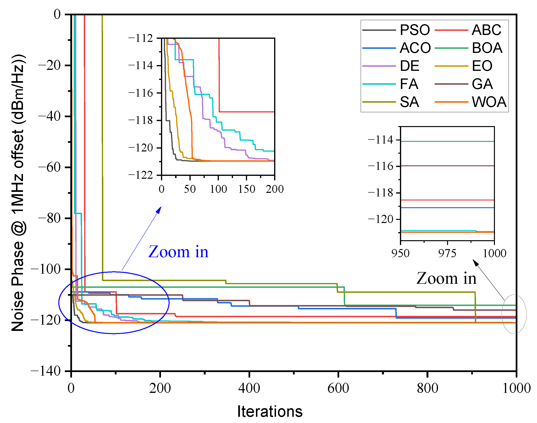
Figure 4 shows the convergence curves for phase noise obtained by the algorithms in the best case, where all algorithms achieved almost the same minimum value. All algorithms demonstrate convergence in fewer than 10 iterations, with DE, ACO, and EO converging after 1, 3, and 4 iterations, respectively.
4.1.2. Scenario 2: Optimize the Entire VCO
The robustness of the results is already reflected in the statistical indicators in
Table 2,
Table 3,
Table 4 and
Table 5 (mean, median, best, worst, standard deviation, success rate). These descriptors provide equivalent insights to boxplot visualizations. Moreover, convergence plots (
Figure 4 and
Figure 5) illustrate the consistency of the algorithms, ensuring statistical soundness without redundant figures.
In this scenario, the varactor and spiral inductor parameters are incorporated as optimization variables integrated into the LC-VCO optimization process. The optimization targets the same oscillation frequency as in Scenario 1, using the same variable ranges for the spiral inductor, varactor, MOS transistors, and current bias.
Table 5 presents a statistical performance comparison of algorithms for the LC-VCO sizing in the second scenario. As in Scenario 1, all algorithms achieved 100% success rates, except for BOA (38%) and GA (23%). PSO, DE, and EO demonstrated exceptional performance, consistently achieving the same optimal value of −120.9616 across all runs, with no variability (standard deviation = 0), indicating perfect consistency. These algorithms also exhibited relatively short convergence times, with EO being the fastest (26.85 s), followed by PSO (40.99 s) and DE (54.12 s). FA, SA, and WOA delivered slightly lower performance values, with FA reaching −120.6275, SA −120.9346, and WOA −120.5234, yet they maintained high consistency, as indicated by their negligible standard deviations, particularly in the case of SA. In contrast, ACO, with a mean of −116.23, was much slower (300.13 s) and showed a small standard deviation (1.09), suggesting that it could be more computationally expensive without a proportional gain in performance. ABC also achieved a competitive mean value (−112.47), but with a higher standard deviation (3.56) and a moderate convergence time (46.47 s). On the other hand, BOA and GA were significantly outperformed, with BOA achieving a mean of −78.88 and GA reaching only −104.46, indicating lower reliability and inferior performance. BOA also exhibited a high variability, shown by a high standard deviation (36.81), suggesting that it may not be a suitable choice for LC-VCO sizing in this scenario. The results suggest that PSO, DE, and EO are the most reliable and efficient algorithms, with DE and EO being particularly fast.
Figure 5 illustrates the convergence curves for phase noise optimization under the best-case scenario, where all algorithms reach their best minimum values. In this scenario, PSO, EO, and WOA demonstrate rapid convergence, completing the process in under 80 iterations. Notably, PSO achieves convergence the fastest, stabilizing before 50 iterations, while EO and WOA follow closely behind, requiring only a few more iterations to converge.
4.1.3. Comparison of Results Between Scenario 1 and Scenario 2
The results of both scenarios highlight key differences in performance and computational time. In Scenario 1, where the inductor and varactor were pre-optimized, all algorithms except GA showed consistent performance with identical phase noise values (−119.91) and zero standard deviation. GA achieved the worst value (−108.92) and had higher variability (2.47). Scenario 2, which involved full optimization of the VCO, resulted in significantly better phase noise performance (−120.96) for PSO, DE, and EO, while ABC, BOA, and GA exhibited greater variability. Computationally, WOA was the fastest algorithm in both scenarios; however, it was not consistent (with 0.98 standard deviation) in Scenario 2. PSO and EO were fast and consistent in both scenarios, while ACO and GA remained the slowest algorithms. Overall, Scenario 2 provided superior phase noise performance due to the inclusion of the varactor and inductor as optimization variables, but at the cost of increased optimization time and complexity, particularly for algorithms like ABC, ACO, BOA, and GA, which struggled with the additional variables.
4.2. Experiment 2: Minimizing Both Phase Noise and Power Consumption
In this experiment, we explore the multi-objective optimization of the complementary cross-coupled LC-VCO circuit, focusing on the trade-off between phase noise and power consumption at a 5 GHz operating frequency. The spiral inductor topology used in previous experiments was maintained. The optimization problem is formulated to simultaneously minimize the two conflicting objectives, resulting in a set of Pareto-optimal solutions. This enables designers to evaluate the trade-offs between phase noise and power consumption, streamlining a more balanced and efficient VCO design that meets the specifications detailed in
Table 6. It should be noted that some of the multi-objective algorithms employed in this study, such as NSGA-II and SPEA2, are mature methods that remain widely used as community benchmarks in analog/RF optimization. Their inclusion allows meaningful comparison with prior LC-VCO optimization studies. At the same time, we also evaluate more recent approaches, including MOEA/D, MOBO/D, and MSSA, which represent modern decomposition-based and swarm-inspired metaheuristics. By combining both classical and emerging methods within a symmetry-aware EKV-driven modeling framework, the present work provides a balanced and up-to-date evaluation that, to the best of our knowledge, has not been previously reported for GHz-range LC-VCO design.
To explore these trade-offs, we use different multi-objective metaheuristics, including Non-dominated Sorting Genetic Algorithm II (NSGA-II), Multi-Objective Particle Swarm Optimization (MOPSO), Strength Pareto Evolutionary Algorithm 2 (SPEA2), Multi-Objective Evolutionary Algorithm Based on Decomposition (MOEA/D), Multi-Objective Optimization Based on Decomposition (MOBO/D), and Multi-objective Salp Swarm Algorithm (MSSA). Each of these algorithms offers unique advantages in balancing the conflicting objectives, and their application allows for a comprehensive evaluation of the solution space. The same design variables and ranges from previous experiments are used, except for the current bias, which is explored over a wider range due to its significant impact on power consumption: .
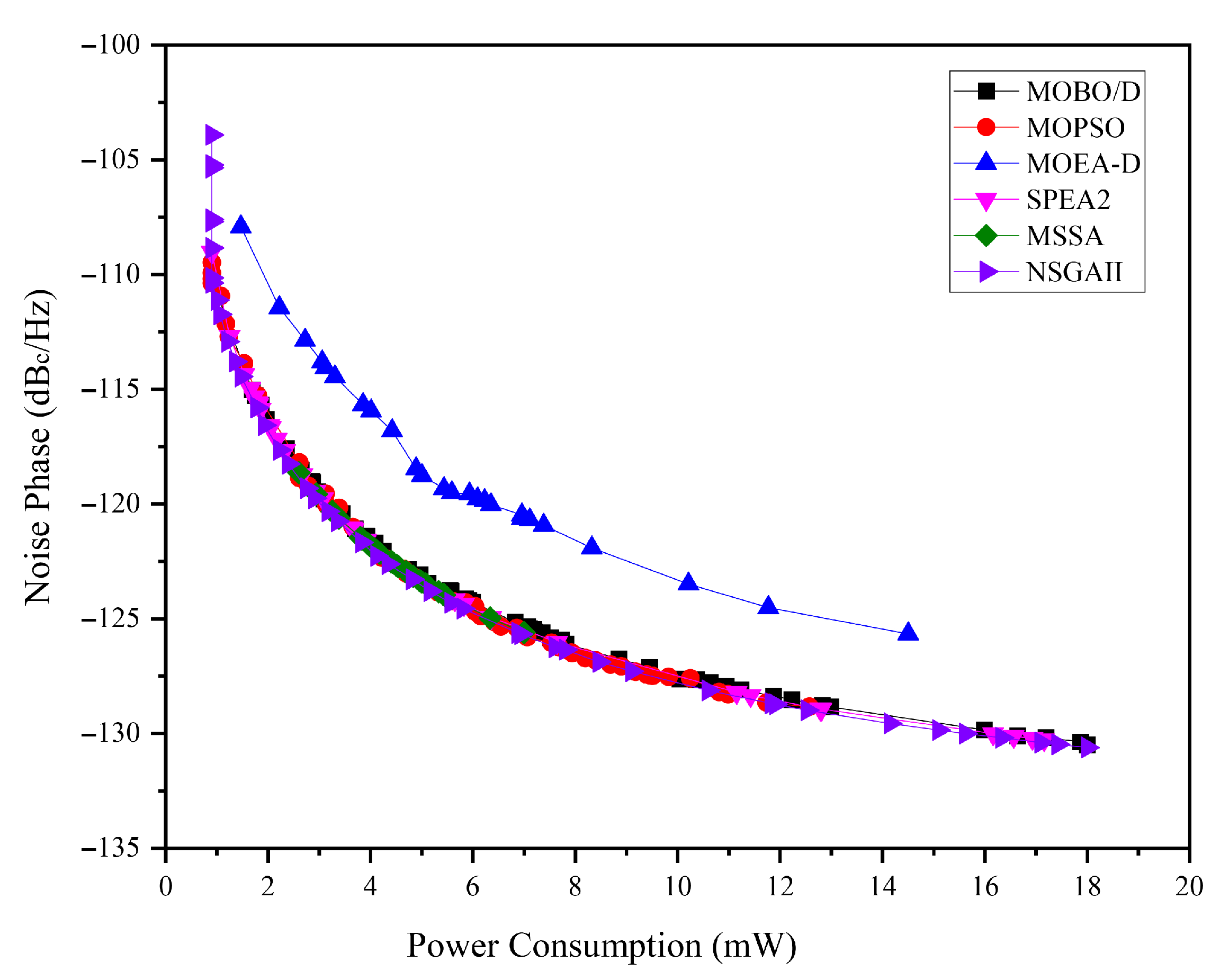
Figure 6 illustrates the combined Pareto fronts generated by the multi-objective metaheuristic algorithms used in this study. The two objectives—minimizing phase noise (dBc/Hz) and power consumption (mW)—represent conflicting trade-offs inherent in the VCO design process. The figure compares the performance of NSGA-II, MOPSO, SPEA2, MOEA/D, MOBO/D, and MSSA. While all algorithms demonstrate well-distributed Pareto fronts, the MOEA/D indicates challenges in achieving both convergence and diversity.
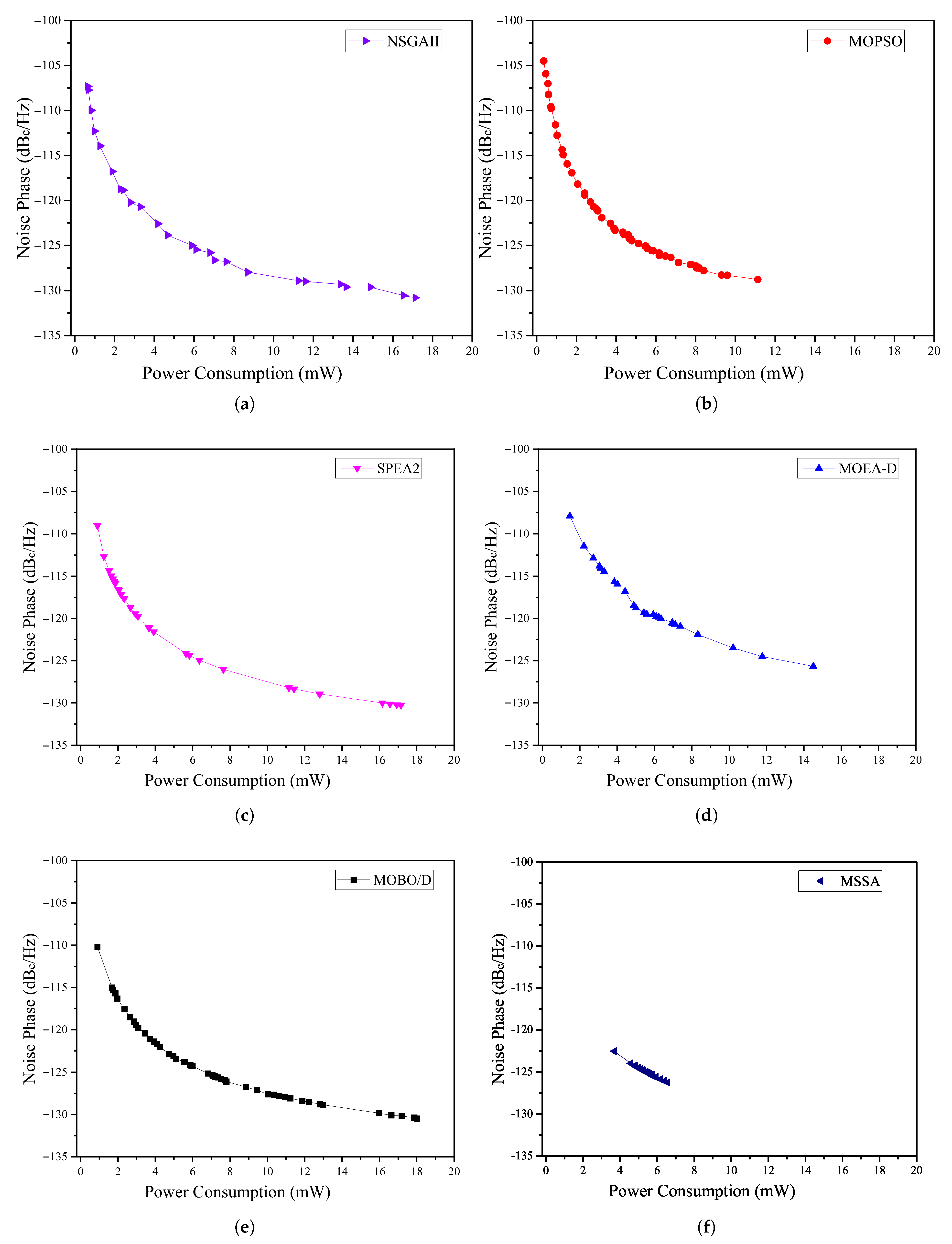
Figure 7 presents the separated Pareto fronts for each algorithm, providing detailed insights into their performance. NSGA-II exhibits a well-distributed front, effectively capturing extreme trade-offs and balancing convergence and diversity. SPEA2 and MOBO/D closely mirror the performance of NSGA-II but provide less smooth fronts with visible gaps, prioritizing convergence over diversity. MOPSO produces a dense front but shows signs of clustering, potentially limiting its ability to maintain a uniform solution spread across the trade-off space. MOEA/D struggles with both convergence and diversity, while MSSA generates a small and but dense front, indicating limited exploration of the objective space and a focus on a specific region.
Overall, the combined and separated Pareto fronts provide valuable insights into the strengths and limitations of each algorithm in handling the conflicting objectives of low phase noise and low power consumption. These results emphasize the importance of selecting algorithms based on the specific requirements of VCO design.
Table 7 presents a comparison of six multi-objective optimization algorithms using three key metrics: convergence time, hypervolume, and IGD. Higher hypervolume and lower IGD values indicate better Pareto front quality.
MSSA achieves the fastest convergence (11.19 s) but yields the least favorable IGD (0.0894) and hypervolume (0.6373). NSGA-II, though the slowest (60.23 s), provides the best overall performance, with the highest hypervolume (0.8343) and the lowest IGD (0), confirming its strength in producing high-quality, well-distributed Pareto fronts.
SPEA2 offers a strong compromise, with the second-best IGD (0.0176), competitive hypervolume (0.8028), and a relatively low convergence time (35.92 s). It stands out as a practical option when balancing solution quality and efficiency.
While MOPSO and MOBO/D converge faster than SPEA2, they deliver inferior Pareto front quality. NSGA-II produces the highest-quality results in terms of IGD and hypervolume, but at the expense of convergence time. In contrast, SPEA2 provides a balanced trade-off between solution quality and computational cost, making it well-suited for applications where both performance and efficiency are important.
Statistical Analysis of Multi-Objective Results
While hypervolume and IGD metrics (
Table 7) provide quantitative measures of Pareto front quality, additional statistical analysis is required to evaluate robustness across multiple runs.
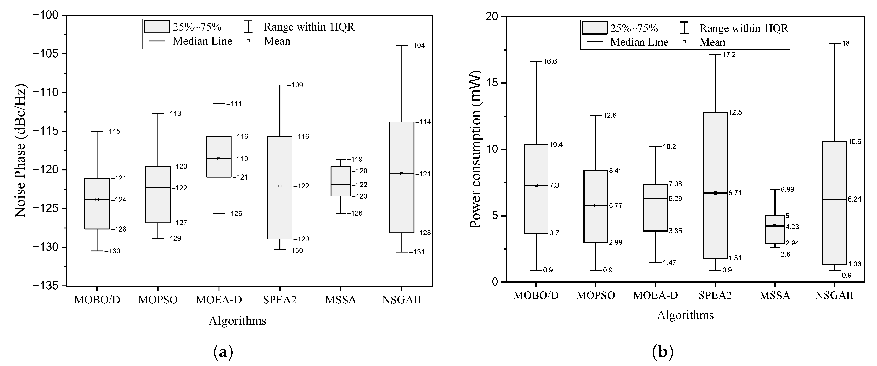
Figure 8 presents boxplots for phase noise (
Figure 8a) and power consumption (
Figure 8b) across the six multi-objective metaheuristics. Each boxplot shows the median (horizontal line), interquartile range (25%–75%, box), mean (square marker), and whiskers, with outliers individually marked.
The boxplots reveal several key observations. NSGA-II and SPEA2 exhibit narrow interquartile ranges, indicating stable performance across runs. NSGA-II achieves consistently low phase noise, confirming its high hypervolume and lowest IGD (
Table 7), while SPEA2 also demonstrates strong robustness. MOPSO and MOBO/D show broader spreads, reflecting higher sensitivity to initial conditions and greater variability. MSSA maintains competitive phase noise levels but shows less variability in power consumption, consistent with the smaller Pareto fronts observed in
Figure 7. MOEA-D presents moderate variability with occasional outliers.
Overall, these boxplots complement the convergence and Pareto front analyses by visually confirming the relative robustness and variability of the tested algorithms, highlighting NSGA-II as the most reliable and SPEA2 as a well-balanced option between performance and efficiency.
4.3. Simulation and Yield Analysis
Since we obtained multiple solutions in both scenarios, we only validated the best-performing solution from
Table 5. The simulation results, shown in
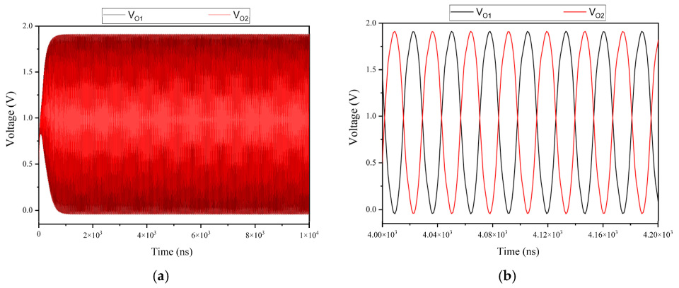
Figure 9, illustrate the output waveforms of the sized CMOS LC-VCO.
Figure 9a presents the complete simulation, capturing both the transient and steady-state behaviors of the oscillator. During the transient phase, the oscillation amplitude gradually increases, demonstrating a successful startup mechanism. In the steady-state phase, the oscillations stabilize at approximately 1.8 V peak-to-peak, indicating robust and reliable operation.
Figure 9b provides a zoomed-in view of the steady-state oscillator behavior. The two differential outputs,
and
, exhibit a periodic waveform with a consistent 180° phase difference. This symmetry confirms the proper functioning of the differential circuit design.
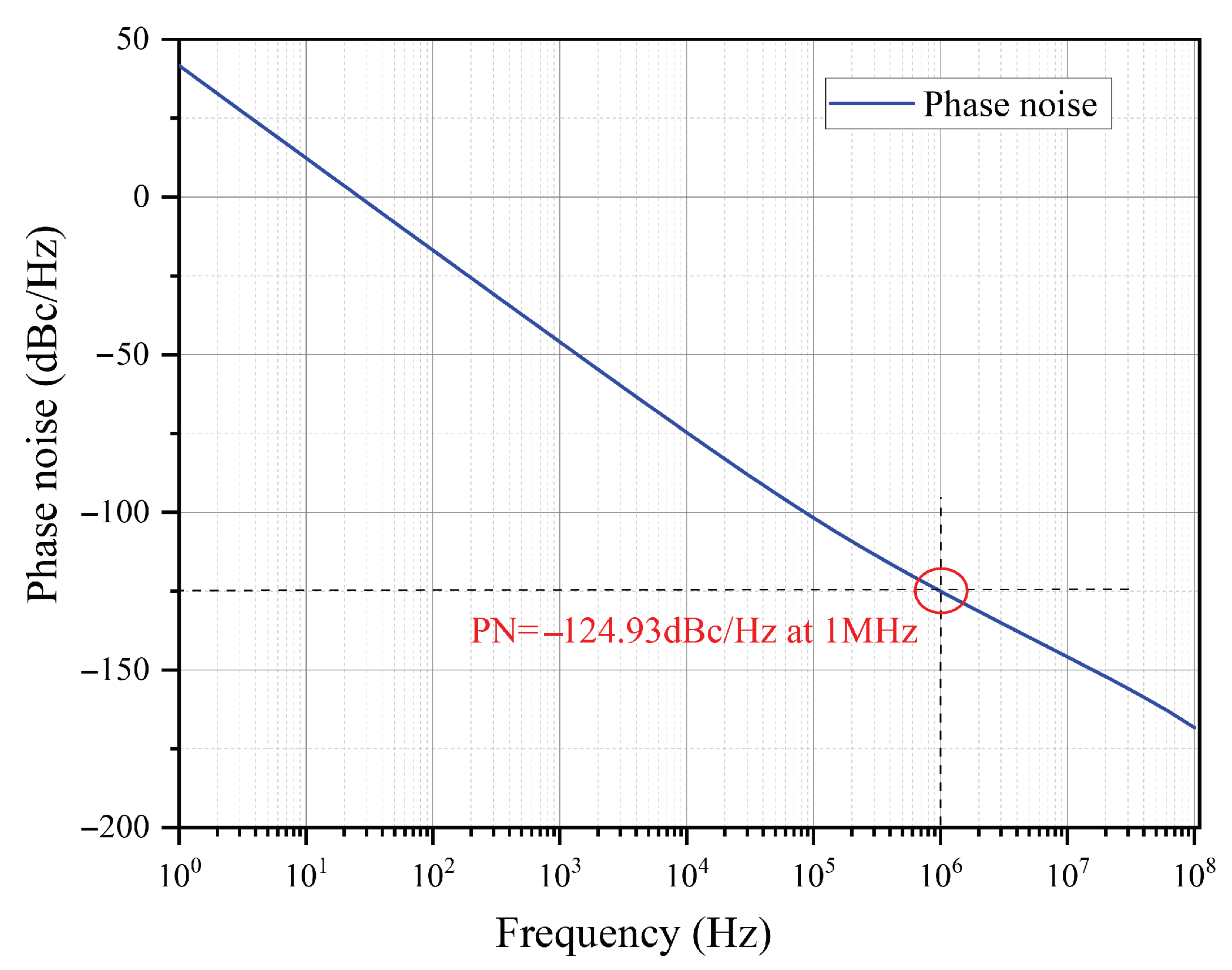
The simulated oscillation frequency of 4.96 GHz and phase noise of
dBc/Hz (see
Figure 10) closely match the targeted design specifications, demonstrating the effectiveness of the proposed setup. These results verify that the CMOS LC-VCO delivers stable oscillations with the intended frequency and amplitude, confirming its suitability for RF and communication applications.
The Monte Carlo simulation results for the LC VCO oscillator provide critical insights into its performance variability across 200 samples. The phase noise distribution (
Figure 11a) demonstrates a tight clustering around the mean value of −124.93 dBc/Hz, with a standard deviation of 56.37 µ, indicating robust noise characteristics within the acceptable design range. Similarly, the oscillation frequency distribution (
Figure 11b) reveals a mean frequency of 4.96113 GHz with minimal deviation (standard deviation of 486.945 MHz), underscoring the stability of the oscillator. Both simulations exhibit 100% pass rates, indicating a high yield that ensures the design consistently meets the performance requirements under process and mismatch variations. These findings validate the effectiveness of the proposed EKV-model-based metaheuristic methodology, reinforcing its potential for high-precision applications and its reliability under diverse operating conditions.
4.4. Symmetry and Asymmetry in EKV-Based VCO Optimization
In high-frequency VCO designs, symmetry is typically sought to ensure phase alignment and minimize common-mode noise. However, the optimization process must address unavoidable asymmetries—such as layout-induced parasitics or finger mismatches—that influence effective capacitance and inductance values.
By embedding physical models (EKV, spiral -model, and parasitic-aware varactor models) into the metaheuristic optimization loop, our approach allows the algorithm to implicitly explore both symmetric and asymmetric configurations. This enables the discovery of Pareto-optimal solutions that either preserve symmetry (for noise minimization) or tolerate controlled asymmetry (for enhanced power efficiency or area reduction).
Moreover, the simulation results show that phase noise minima often correspond to symmetric sizing conditions, whereas power minimization occasionally yields asymmetrical transistor biasing or LC tank element dimensions. This interplay reinforces the importance of considering symmetry and asymmetry as part of AI-driven optimization strategies.
5. Conclusions
In this paper, we introduced an automated sizing methodology for a complementary cross-coupled CMOS LC-VCO circuit, using the EKV model and metaheuristic optimization algorithms. The VCO is fully modeled through analytical equations and a technology-specific EKV model, offering a high degree of adaptability to emerging technologies and significantly faster computation than traditional electromagnetic simulation-based methods.
Two distinct scenarios were explored for single-objective optimization: (1) optimizing the LC tank (varactor and spiral inductor) as a preliminary step, followed by LC-VCO optimization using the fixed LC tank parameters; and (2) treating the varactor and spiral inductor as design variables integrated within the LC-VCO optimization. Metaheuristic algorithms proved highly effective in navigating the complex design space, particularly in addressing the sensitivity of on-chip LC tank quality factors to degradation, which directly impacts phase noise.
We further extended the methodology to multi-objective optimization, simultaneously minimizing phase noise and power consumption. Among the various algorithms tested, NSGA-II achieved the most balanced trade-off between Pareto front quality and diversity. These results underscore the suitability of multi-objective metaheuristics in resolving conflicting design goals.
To validate robustness under manufacturing variations, Monte Carlo simulations were conducted on the best-performing solution. The results demonstrated excellent yield, with a 100% pass rate for both phase noise and oscillation frequency specifications across 200 samples, confirming the method’s ability to indicate robustness under evaluated scenarios. The optimized LC-VCO achieved a mean phase noise of −124.93 dBc/Hz and an oscillation frequency centered around 4.96 GHz with minimal deviation, confirming the method’s ability to meet stringent RF performance requirements.
In summary, the proposed methodology effectively minimizes phase noise and power consumption, providing a scalable and accurate solution for analog circuit sizing in advanced CMOS technologies. The novelty of this work lies not in proposing a new optimization algorithm but in embedding symmetry/asymmetry considerations into EKV-based analytical modeling, thereby enabling existing algorithms to achieve physically consistent and verifiable LC-VCO designs.
This distinction is crucial: while many recent works focus on creating new metaheuristic variants, our contribution addresses the equally important gap of providing a physically grounded, symmetry-aware modeling framework that makes optimization results meaningful for real CMOS implementations. In this way, the proposed methodology complements ongoing algorithmic innovations by ensuring that both classical and modern optimizers produce designs that are not only optimal in theory but also valid and verifiable in practice.
Our study complements recent survey findings by demonstrating how a symmetry-aware EKV modeling layer can be combined with both classical and modern metaheuristics (including hybrid, surrogate-assisted, and decomposition-based approaches) to produce physically consistent and efficient LC-VCO designs while keeping simulation cost tractable.
Crucially, beyond its algorithmic effectiveness, this work emphasizes the implicit handling of structural symmetry and asymmetry in RF circuit design. While symmetric topologies ensure balanced performance, asymmetries arising from parasitics or design constraints can be strategically exploited within the optimization framework. By relying on physically grounded models and algorithmic intelligence, the proposed method aligns with the broader goals of symmetry-aware EDA, offering a practical approach to balancing regularity and deviation in high-performance analog systems.
