
Superconductivity in Hierarchical 3D Nanostructured Pb–In Alloys

 ,
,  , and
, and 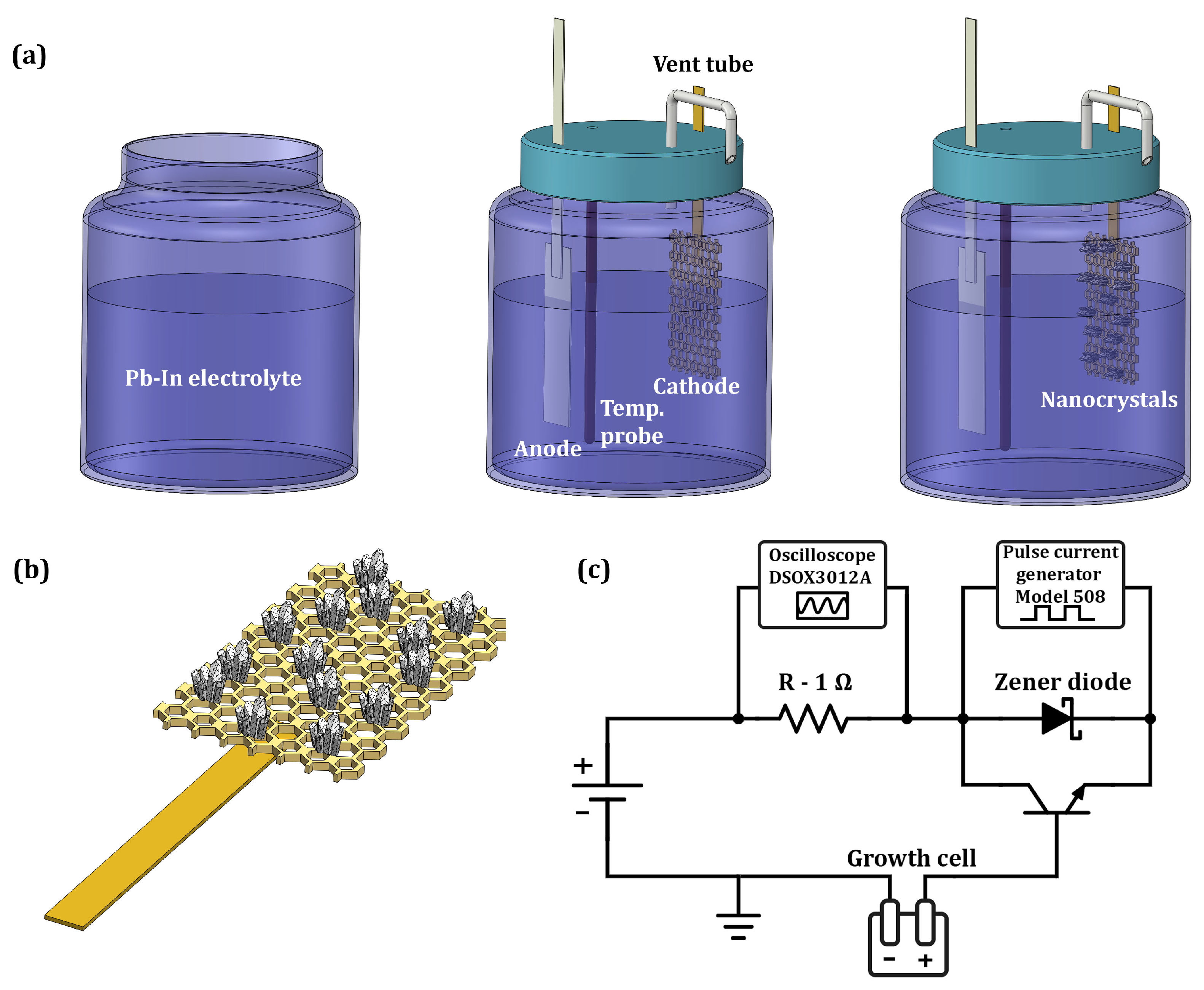
Abstract
1. Introduction
2. Methods
3. Results and Discussion
3.1. Sample Structures
3.2. Dynamic Magnetic Susceptibility of Pb–In Nanocrystalline Samples
3.2.1. Theory
3.2.2. Results of Measurement and Calculation
4. Conclusions
Author Contributions
Funding
Data Availability Statement
Acknowledgments
Conflicts of Interest
References
- Bose, S.; Ayyub, P. A review of finite size effects in quasi-zero dimensional superconductors. Rep. Prog. Phys. 2014, 77, 116503. [Google Scholar] [CrossRef]
- Arutyunov, K.Y.; Golubev, D.S.; Zaikin, A.D. Superconductivity in one dimension. Phys. Rep. 2008, 464, 1–70. [Google Scholar] [CrossRef]
- Brun, C.; Cren, T.; Roditchev, D. Review of 2D superconductivity: The ultimate case of epitaxial monolayers. Supercond. Sci. Technol. 2016, 30, 013003. [Google Scholar] [CrossRef]
- Alam, H.; Ramakrishna, S. A review on the enhancement of figure of merit from bulk to nano-thermoelectric materials. Nano Energy 2013, 2, 190–212. [Google Scholar] [CrossRef]
- Yeom, S.H.; Kang, B.H.; Kim, K.J.; Kang, S.W. Nanostructures in biosensor—A review. Front.-Biosci.-Landmark 2011, 16, 997–1023. [Google Scholar] [CrossRef]
- Yakovlev, D.S.; Lvov, D.S.; Emelyanova, O.V.; Dzhumaev, P.S.; Shchetinin, I.V.; Skryabina, O.V.; Egorov, S.V.; Ryazanov, V.V.; Golubov, A.A.; Roditchev, D.; et al. Physical Vapor Deposition Features of Ultrathin Nanocrystals of Bi2(Tex Se1−x)3. J. Phys. Chem. Lett. 2022, 13, 9221–9231. [Google Scholar] [CrossRef] [PubMed]
- Lee, J.H.; Singer, J.P.; Thomas, E.L. Micro-/nanostructured mechanical metamaterials. Adv. Mater. 2012, 24, 4782–4810. [Google Scholar] [CrossRef] [PubMed]
- Kalidindi, S.B.; Jagirdar, B.R. Nanocatalysis and prospects of green chemistry. ChemSusChem 2012, 5, 65–75. [Google Scholar] [CrossRef]
- Sacépé, B.; Feigel’man, M.; Klapwijk, T.M. Quantum breakdown of superconductivity in low-dimensional materials. Nat. Phys. 2020, 16, 734–746. [Google Scholar] [CrossRef]
- Anderson, P.W. Theory of dirty superconductors. J. Phys. Chem. Solids 1959, 11, 26–30. [Google Scholar] [CrossRef]
- von Delft, J.; Zaikin, A.D.; Golubev, D.S.; Tichy, W. Parity-affected superconductivity in ultrasmall metallic grains. Phys. Rev. Lett. 1996, 77, 3189. [Google Scholar] [CrossRef] [PubMed]
- Smith, R.A.; Ambegaokar, V. Effect of level statistics on superconductivity in ultrasmall metallic grains. Phys. Rev. Lett. 1996, 77, 4962. [Google Scholar] [CrossRef] [PubMed]
- Bezryadin, A. Quantum suppression of superconductivity in nanowires. J. Physics Condens. Matter 2008, 20, 043202. [Google Scholar] [CrossRef]
- Natarajan, C.M.; Tanner, M.G.; Hadfield, R.H. Superconducting nanowire single-photon detectors: Physics and applications. Supercond. Sci. Technol. 2012, 25, 063001. [Google Scholar] [CrossRef]
- Xing, Y.; Sun, Y.; Singh, M.; Zhao, Y.F.; Chan, M.H.; Wang, J. Electronic transport properties of topological insulator films and low dimensional superconductors. Front. Phys. 2013, 8, 491–508. [Google Scholar] [CrossRef]
- Franca, S.; Efremov, D.; Fulga, I. Phase-tunable second-order topological superconductor. Phys. Rev. B 2019, 100, 075415. [Google Scholar] [CrossRef]
- Grünhaupt, L.; Spiecker, M.; Gusenkova, D.; Maleeva, N.; Skacel, S.T.; Takmakov, I.; Valenti, F.; Winkel, P.; Rotzinger, H.; Wernsdorfer, W.; et al. Granular aluminium as a superconducting material for high-impedance quantum circuits. Nat. Mater. 2019, 18, 816–819. [Google Scholar] [CrossRef]
- Ekinci, K.; Valles, J., Jr. Morphology of quench condensed Pb films near the insulator to metal transition. Phys. Rev. Lett. 1999, 82, 1518. [Google Scholar] [CrossRef]
- Guo, Y.; Zhang, Y.F.; Bao, X.Y.; Han, T.Z.; Tang, Z.; Zhang, L.X.; Zhu, W.G.; Wang, E.; Niu, Q.; Qiu, Z.; et al. Superconductivity modulated by quantum size effects. Science 2004, 306, 1915–1917. [Google Scholar] [CrossRef]
- Moshchalkov, V.; Gielen, L.; Strunk, C.; Jonckheere, R.; Qiu, X.; Haesendonck, C.V.; Bruynseraede, Y. Effect of sample topology on the critical fields of mesoscopic superconductors. Nature 1995, 373, 319–322. [Google Scholar] [CrossRef]
- Zgirski, M.; Riikonen, K.P.; Touboltsev, V.; Arutyunov, K. Size dependent breakdown of superconductivity in ultranarrow nanowires. Nano Lett. 2005, 5, 1029–1033. [Google Scholar] [CrossRef] [PubMed]
- Reich, S.; Leitus, G.; Popovitz-Biro, R.; Schechter, M. Magnetization of small lead particles. Phys. Rev. Lett. 2003, 91, 147001. [Google Scholar] [CrossRef] [PubMed]
- Li, W.H.; Yang, C.; Tsao, F.; Lee, K. Quantum size effects on the superconducting parameters of zero-dimensional Pb nanoparticles. Phys. Rev. B 2003, 68, 184507. [Google Scholar] [CrossRef]
- Tsai, A.; Chandrasekhar, N.; Chattopadhyay, K. Size effect on the superconducting transition of embedded lead particles in an Al–Cu–V amorphous matrix. Appl. Phys. Lett. 1999, 75, 1527–1528. [Google Scholar] [CrossRef]
- Li, W.H.; Yang, C.; Tsao, F.; Wu, S.; Huang, P.; Chung, M.; Yao, Y. Enhancement of superconductivity by the small size effect in In nanoparticles. Phys. Rev. B 2005, 72, 214516. [Google Scholar] [CrossRef]
- Wu, F.Y.; Yang, C.; Wu, C.M.; Wang, C.W.; Li, W.H. Superconductivity in zero-dimensional indium nanoparticles. J. Appl. Phys. 2007, 101, 09G111. [Google Scholar] [CrossRef]
- Profeta, G.; Calandra, M.; Mauri, F. Phonon-mediated superconductivity in graphene by lithium deposition. Nat. Phys. 2012, 8, 131–134. [Google Scholar] [CrossRef]
- Szczȩśniak, D.; Szczȩśniak, R. Signatures of nonadiabatic superconductivity in lithium-decorated graphene. Phys. Rev. B 2019, 99, 224512. [Google Scholar] [CrossRef]
- Strukova, G.K.; Strukov, G.V.; Postnova, E.Y.; Rusanov, A.Y.; Veshchunov, I.S. Mesoscopic models of plants composed of metallic nanowires. J. Bionic Eng. 2013, 10, 368–376. [Google Scholar] [CrossRef][Green Version]
- Sun, L.L.; Liu, L.L.; Luo, L.H.; Wu, Y.F.; Shi, J.J.; Cheng, L.; Xu, X.U.; Guo, Y.M. Facile synthesis of flower-like Pd catalyst for direct ethanol solid oxide fuel cell. J. Fuel Chem. Technol. 2016, 44, 607–612. [Google Scholar] [CrossRef]
- Li, K.; Teng, H.; Dai, X.; Wang, Y.; Wang, D.; Zhang, X.; Yao, Y.; Liu, X.; Feng, L.; Rao, J.; et al. Atomic scale modulation strategies and crystal phase transition of flower-like CoAl layered double hydroxides for supercapacitors. CrystEngComm 2022, 24, 2081–2088. [Google Scholar] [CrossRef]
- Fu, M.; Zhu, Z.; Chen, W.; Yu, H.; Lv, R. Carbon cloth-supported flower-like porous nickel-based electrodes boosting ion/charge transfer characteristics of flexible supercapacitors. Carbon 2022, 199, 520–528. [Google Scholar] [CrossRef]
- Riminucci, A.; Schwarzacher, W. Magnetic signature of granular superconductivity in electrodeposited Pb nanowires. J. Appl. Phys. 2014, 115, 223910. [Google Scholar] [CrossRef]
- Strukova, G.; Strukov, G.; Khodos, I.; Vitkalov, S. Disintegration of nanostructured metals with the formation of nanoparticles in electron microscope. Nano-Struct. Nano-Objects 2018, 16, 104–109. [Google Scholar] [CrossRef]
- Neminsky, A.; Nikolaev, P.; Shovkun, D.; Laukhina, E.; Yagubskii, E. Temperature dependence of the magnetic field penetration depth in Rb 3 C 60 measured by ac susceptibility. Phys. Rev. Lett. 1994, 72, 3092. [Google Scholar] [CrossRef] [PubMed]
- Imai, Y.; Nabeshima, F.; Yoshinaka, T.; Miyatani, K.; Kondo, R.; Komiya, S.; Tsukada, I.; Maeda, A. Superconductivity at 5.4 K in β-Bi2Pd. J. Phys. Soc. Jpn. 2012, 81, 113708. [Google Scholar] [CrossRef]
- Shmyt’ko, I.; Kudrenko, E.; Strukova, G.; Klassen, N. “Isomorphous” phases in nanodispersed powders of rare-earth oxides. Phys. Solid State 2008, 50, 1157–1164. [Google Scholar] [CrossRef]
- Shmyt’ko, I.; Strukova, G. Fine sructure of Na5Lu9F32 nanocrystallites formed at the initial stages of crystallization. Phys. Solid State 2009, 51, 1907–1911. [Google Scholar] [CrossRef]
- Williamson, G.; Hall, W. X-ray line broadening from filed aluminium and wolfram. Acta Metall. 1953, 1, 22–31. [Google Scholar] [CrossRef]
- Guinier, A. X-ray Diffraction in Crystals, Imperfect Crystals, and Amorphous Bodies; Courier Corporation: Chelmsford, MA, USA, 1994. [Google Scholar]
- Liz-Marzan, L.M.; Kamat, P.V. Nanoscale Materials; Springer: Berlin/Heidelberg, Germany, 2004; pp. 1–3. [Google Scholar]
- Landau, L.; Lifshitz, E. Electrodynamics of Condensed Matter; Nauka: Moscow, Russia, 1982. [Google Scholar]
- Rao, C.; Dubeck, L.; Rothwarf, F. Superconducting energy gaps from magnetization measurements: Pb-In system. Phys. Rev. B 1973, 7, 1866. [Google Scholar] [CrossRef]


Publisher’s Note: MDPI stays neutral with regard to jurisdictional claims in published maps and institutional affiliations. |
© 2022 by the authors. Licensee MDPI, Basel, Switzerland. This article is an open access article distributed under the terms and conditions of the Creative Commons Attribution (CC BY) license (https://creativecommons.org/licenses/by/4.0/).
Share and Cite
Shevchun, A.F.; Strukova, G.K.; Shmyt’ko, I.M.; Strukov, G.V.; Vitkalov, S.A.; Yakovlev, D.S.; Nazhestkin, I.A.; Shovkun, D.V. Superconductivity in Hierarchical 3D Nanostructured Pb–In Alloys. Symmetry 2022, 14, 2142. https://doi.org/10.3390/sym14102142
Shevchun AF, Strukova GK, Shmyt’ko IM, Strukov GV, Vitkalov SA, Yakovlev DS, Nazhestkin IA, Shovkun DV. Superconductivity in Hierarchical 3D Nanostructured Pb–In Alloys. Symmetry. 2022; 14(10):2142. https://doi.org/10.3390/sym14102142
Chicago/Turabian StyleShevchun, Artem F., Galina K. Strukova, Ivan M. Shmyt’ko, Gennady V. Strukov, Sergey A. Vitkalov, Dmitry S. Yakovlev, Ivan A. Nazhestkin, and Dmitry V. Shovkun. 2022. "Superconductivity in Hierarchical 3D Nanostructured Pb–In Alloys" Symmetry 14, no. 10: 2142. https://doi.org/10.3390/sym14102142
APA StyleShevchun, A. F., Strukova, G. K., Shmyt’ko, I. M., Strukov, G. V., Vitkalov, S. A., Yakovlev, D. S., Nazhestkin, I. A., & Shovkun, D. V. (2022). Superconductivity in Hierarchical 3D Nanostructured Pb–In Alloys. Symmetry, 14(10), 2142. https://doi.org/10.3390/sym14102142