
Efficient Designs of Quantum Adder/Subtractor Using Universal Reversible Gate on IBM Q


Abstract
:1. Introduction
2. Preliminaries
2.1. Basic Definitions
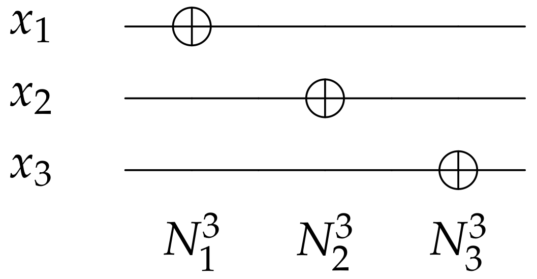
2.1.1. NOT Gate
2.1.2. Feynman Gate
2.1.3. Controlled Square-Root NOT Gate
2.1.4. Toffoli Gate
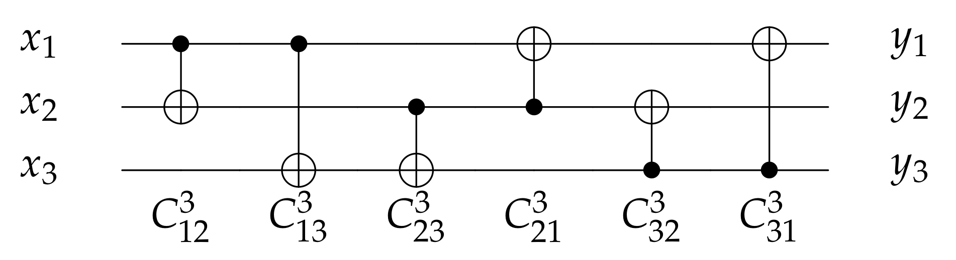
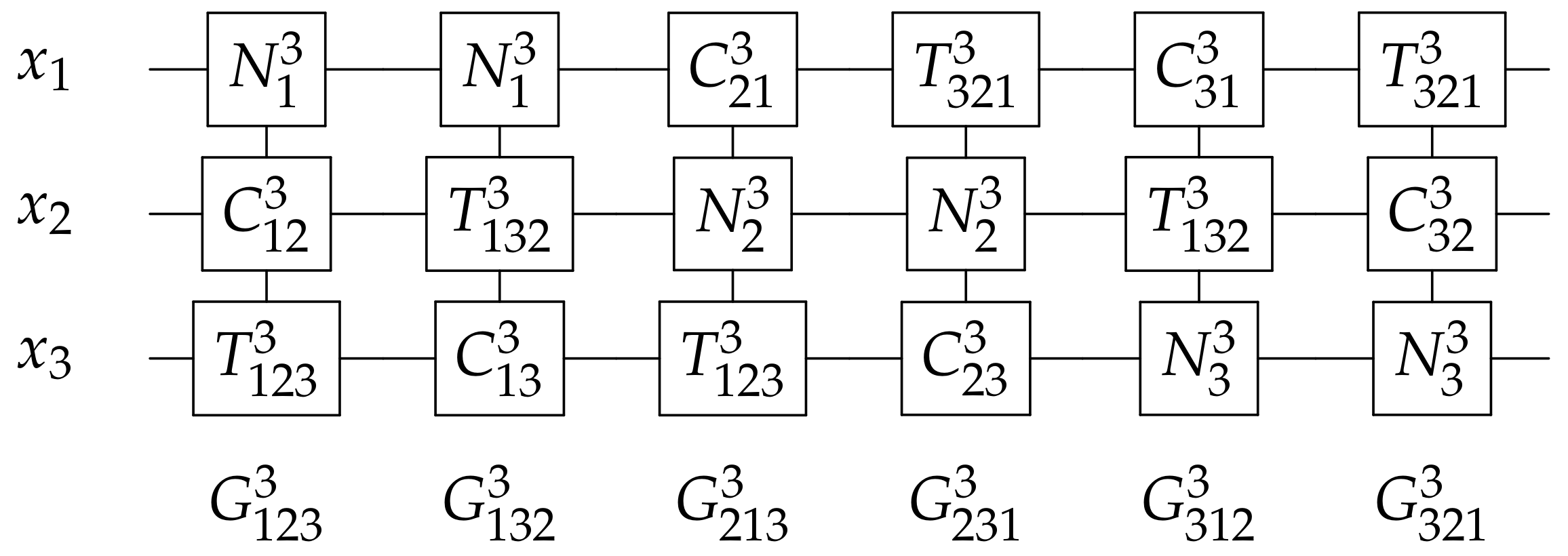
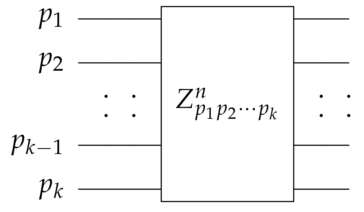
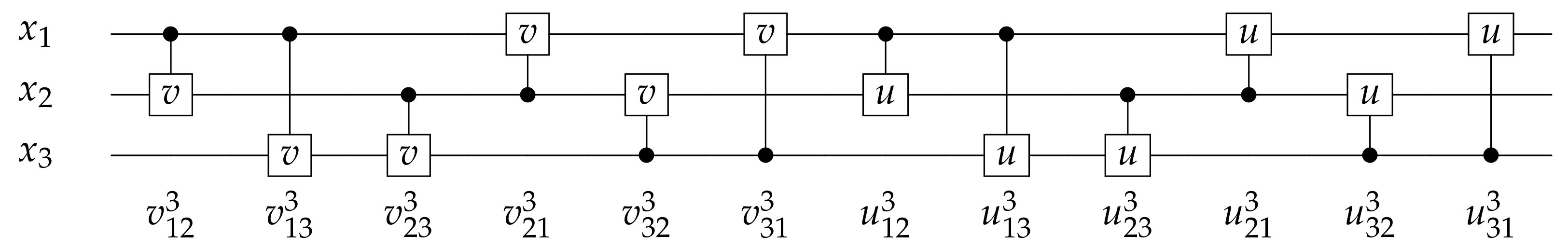
2.1.5. G Gate
- Every () or () quantum gates will have only one unit delay.
- Every quantum gates with () or bigger will be substituted with their equivalent () gates and () gates.
- Find the path from input to output which has the maximum delay; this is considered the unit delay of the circuit.
3. The Proposed Designs
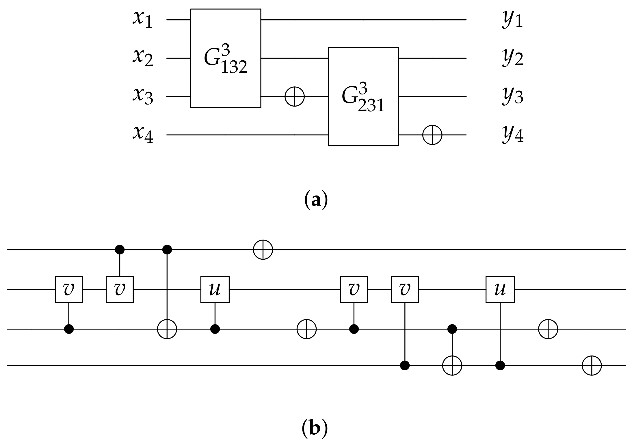
3.1. The Proposed Reversible Half Adder/Subtractor Circuits
3.2. The Proposed Reversible Full Adder Circuit
3.3. The Proposed Reversible Full Subtractor Circuit
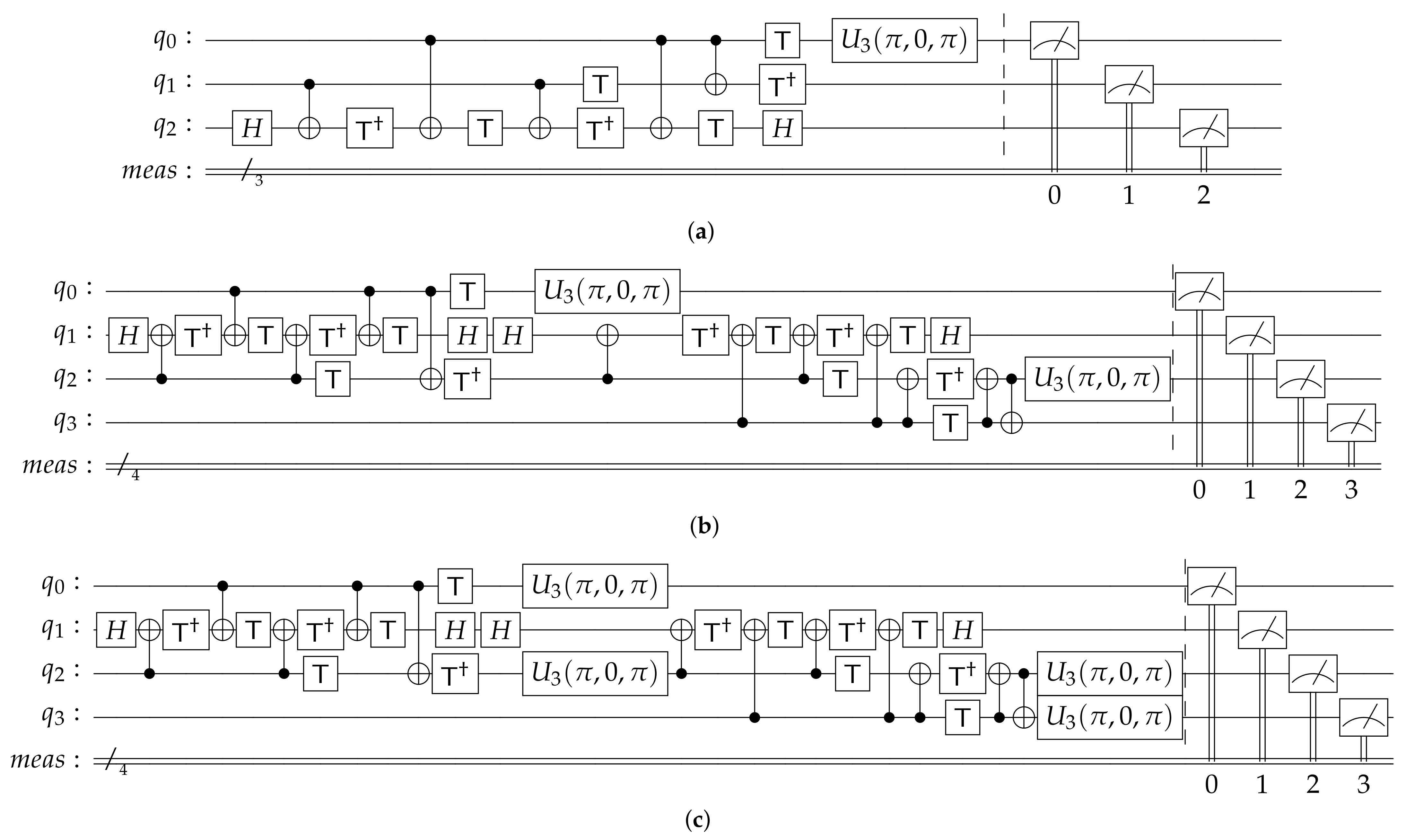
4. Experimental Results and Discussion
Executing the Proposed Designs on IBM Q
5. Conclusions
Author Contributions
Funding
Institutional Review Board Statement
Informed Consent Statement
Data Availability Statement
Acknowledgments
Conflicts of Interest
References
- Bennett, C.H. Logical reversibility of computation. IBM J. Res. Dev. 1973, 17, 525–532. [Google Scholar] [CrossRef]
- Fredkin, E.; Toffoli, T. Conservative logic. Int. J. Theor. Phys. 1982, 21, 219–253. [Google Scholar] [CrossRef]
- Garipelly, R.; Kiran, P.M.; Kumar, A.S. A review on reversible logic gates and their implementation. Int. J. Emerg. Technol. Adv. Eng. 2013, 3, 417–423. [Google Scholar]
- De Vos, A.; Desoete, B.; Janiak, F.; Nogawski, A. Control Gates as Building Blocks for Reversible Computers; Proceedings Patmos 2001 Conference; Springer: New York, NY, USA, 2001. [Google Scholar]
- De Vos, A.; Desoete, B.; Adamski, A.; Pietrzak, P.; Sibiński, M.; Widerski, T. Design of reversible logic circuits by means of control gates. In International Workshop on Power and Timing Modeling, Optimization and Simulation; Springer: Berlin/Heidelberg, Germany, 2000; pp. 255–264. [Google Scholar]
- Orlov, A.; Amlani, I.; Bernstein, G.; Lent, C.; Snider, G. Realization of a functional cell for quantum-dot cellular automata. Science 1997, 277, 928–930. [Google Scholar] [CrossRef] [Green Version]
- Amlani, I.; Orlov, A.O.; Toth, G.; Bernstein, G.H.; Lent, C.S.; Snider, G.L. Digital logic gate using quantum-dot cellular automata. Science 1999, 284, 289–291. [Google Scholar] [CrossRef] [PubMed] [Green Version]
- Feynman, R.P. Quantum mechanical computers. Found. Phys. 1986, 16, 507–531. [Google Scholar] [CrossRef]
- Deutsch, D. Quantum theory, the Church–Turing principle and the universal quantum computer. Proc. R. Soc. London. A Math. Phys. Sci. 1985, 400, 97–117. [Google Scholar]
- Lloyd, S. A potentially realizable quantum computer. Science 1993, 261, 1569–1571. [Google Scholar] [CrossRef] [PubMed]
- Buhrman, H.; Cleve, R.; Wigderson, A. Quantum vs. classical communication and computation. In Proceedings of the Thirtieth Annual ACM Symposium on Theory of Computing, Dallas, TX, USA, 24–26 May 1998; pp. 63–68. [Google Scholar]
- Grover, L.K. Quantum mechanics helps in searching for a needle in a haystack. Phys. Rev. Lett. 1997, 79, 325. [Google Scholar] [CrossRef] [Green Version]
- Shor, P.W. Polynomial-time algorithms for prime factorization and discrete logarithms on a quantum computer. SIAM Rev. 1999, 41, 303–332. [Google Scholar] [CrossRef]
- Nielsen, M.A.; Chuang, I. Quantum Computation and Quantum Information; Cambridge University Press: Cambridge, UK, 2002. [Google Scholar]
- Mohammadi, M.; Eshghi, M. On figures of merit in reversible and quantum logic designs. Quantum Inf. Process. 2009, 8, 297–318. [Google Scholar] [CrossRef]
- Patterson, D.A.; Hennessy, J.L. Computer Organization and Design ARM Edition: The Hardware Software Interface; Morgan Kaufmann: San Francisco, CA, USA, 2016. [Google Scholar]
- Thapliyal, H.; Ranganathan, N. A new design of the reversible subtractor circuit. In Proceedings of the 2011 11th IEEE International Conference on Nanotechnology, Portland, OR, USA, 15–18 August 2011; pp. 1430–1435. [Google Scholar]
- Gupta, A.; Singla, P.; Gupta, J.; Maheshwari, N. An improved structure of reversible adder and subtractor. arXiv 2013, arXiv:1306.1889. [Google Scholar]
- Moghimi, S.; Reshadinezhad, M.R. A Novel 4*4 Universal Reversible Gate as a Cost Efficient Full Adder/Subtractor in Terms of Reversible and Quantum Metrics. Int. J. Mod. Educ. Comput. Sci. 2015, 7. [Google Scholar] [CrossRef] [Green Version]
- Montaser, R.; Younes, A.; Abdel-Aty, M. New design of reversible full adder/subtractor using R gate. Int. J. Theor. Phys. 2019, 58, 167–183. [Google Scholar] [CrossRef] [Green Version]
- Younes, A. On the universality of n-bit reversible gate libraries. Appl. Math. Inf. Sci. 2015, 9, 2579. [Google Scholar]
- Montaser, R.; Younes, A.; Abdel-Aty, M. New Design of Universal Reversible Gate Library. Quantum Matter 2017, 6, 89–96. [Google Scholar] [CrossRef]
- Osman, M.; Younes, A.; Ismail, G.; Farouk, R. An Improved Design of n-Bit Universal Reversible Gate Library. Int. J. Theor. Phys. 2019, 58, 2531–2549. [Google Scholar] [CrossRef]
- Team I.Q. IBM Q 5 Santiago Backend Specification V1.0.0; IBM: Armonk, NY, USA, 2018. [Google Scholar]
- Qiskit: An Open-source Framework for Quantum Computing. 2019. Available online: https://qiskit.org/ (accessed on 8 August 2021).
- Mano, M.M.; Ciletti, M. Digital Design: With an Introduction to the Verilog HDL; Pearson: New York, NY, USA, 2013. [Google Scholar]
- Katz, R.H.; Borriello, G. Contemporary Logic Design. 2005. Available online: https://www.amazon.com/Contemporary-Logic-Design-Randy-Katz/dp/0201308576 (accessed on 8 August 2021).
- Yang, G.; Song, X.; Perkowski, M.A.; Hung, W.N.; Seo, C.J. Minimal universal library for n× n reversible circuits. Comput. Math. Appl. 2008, 56, 160–165. [Google Scholar] [CrossRef] [Green Version]
- Toffoli, T. Reversible computing. In International Colloquium on Automata, Languages, and Programming; Springer: Berlin/Heidelberg, Germany, 1980; pp. 632–644. [Google Scholar]
- Montaser, R.; Younes, A.; Abdel-Aty, M. Improving the quantum cost of NCT-based reversible circuit. Quantum Inf. Process. 2015, 14, 1249–1263. [Google Scholar] [CrossRef]
- Ali, M.B.; Hirayama, T.; Yamanaka, K.; Nishitani, Y. Quantum cost reduction of reversible circuits using new Toffoli decomposition techniques. In Proceedings of the 2015 International Conference on Computational Science and Computational Intelligence (CSCI), Las Vegas, NV, USA, 7–9 December 2015; pp. 59–64. [Google Scholar]
- Shende, V.V.; Prasad, A.K.; Markov, I.L.; Hayes, J.P. Synthesis of reversible logic circuits. IEEE Trans. Comput.-Aided Des. Integr. Circuits Syst. 2003, 22, 710–722. [Google Scholar] [CrossRef] [Green Version]
- Maslov, D.; Miller, D.M. Comparison of the cost metrics for reversible and quantum logic synthesis. arXiv 2005, arXiv:quant-ph/0511008. [Google Scholar]
- Yang, G.; Song, X.; Hung, W.N.; Perkowski, M.A.; Seo, C.J. Synthesis of reversible circuits with minimal costs. Calcolo 2008, 45, 193–206. [Google Scholar] [CrossRef]
- Ni, L.; Guan, Z.; Zhu, W. A general method of constructing the reversible full-adder. In Proceedings of the 2010 Third International Symposium on Intelligent Information Technology and Security Informatics, Jian, China, 2–4 April 2010; pp. 109–113. [Google Scholar]
- Morrison, M.; Ranganathan, N. Design of a reversible ALU based on novel programmable reversible logic gate structures. In Proceedings of the 2011 IEEE Computer Society Annual Symposium on VLSI, Chennai, India, 4–6 July 2011; pp. 126–131. [Google Scholar]
- Rangaraju, H.; Venugopal, U.; Muralidhara, K.; Raja, K. Design of efficient reversible parallel Binary adder/subtractor. In International Conference on Advances in Communication, Network, and Computing; Springer: Berlin/Heidelberg, Germany, 2011; pp. 83–87. [Google Scholar]
- Bruce, J.; Thornton, M.A.; Shivakumaraiah, L.; Kokate, P.; Li, X. Efficient adder circuits based on a conservative reversible logic gate. In Proceedings of the IEEE Computer Society Annual Symposium on VLSI. New Paradigms for VLSI Systems Design (ISVLSI 2002), Pittsburgh, PA, USA, 25–26 April 2002; pp. 83–88. [Google Scholar]
- Babu, H.M.H.; Islam, M.R.; Chowdhury, S.M.A.; Chowdhury, A.R. Synthesis of full-adder circuit using reversible logic. In Proceedings of the 17th International Conference on VLSI Design. Proceedings, Mumbai, India, 9 January 2004; pp. 757–760. [Google Scholar]
- Thapliyal, H.; Srinivas, M. A new reversible TSG gate and its application for designing efficient adder circuits. arXiv 2006, arXiv:cs/0603091. [Google Scholar]


| Result | |||||||
|---|---|---|---|---|---|---|---|
| Proposed design Section 3.1 | 0 | ADD, NOT | |||||
| SUB, NOT |
| Result | |||||||||
|---|---|---|---|---|---|---|---|---|---|
| Proposed design Section 3.2 | Sum | ADD, NOT, XNOR | |||||||
| NOT, AND, XNOR, XOR | |||||||||
| NOT, OR, XNOR | |||||||||
| NOT, NAND, XNOR, XOR | |||||||||
| NOT, NOR, XNOR, XOR | |||||||||
| Proposed design Section 3.3 | Difference | SUB, NOT, XOR |
| SUM | Success Probability | |||
|---|---|---|---|---|
| Average success probability | ||||
| Diff | Success Probability | |||
|---|---|---|---|---|
| Average success probability | ||||
| SUM | Success Probability | ||||
|---|---|---|---|---|---|
| Average success probability | |||||
| Diff | Success Probability | ||||
|---|---|---|---|---|---|
| Average success probability | |||||
| Reference | Function | QC | GO | CI | GC | Delay |
|---|---|---|---|---|---|---|
| Proposed designSection 3.2 | FA | |||||
| Proposed designSection 3.3 | FS | |||||
| [35] | FA | − | − | |||
| [36] | FA/FS | |||||
| Design 1 [37] | FA/FS | − | ||||
| Design 2 [37] | FA/FS | − | ||||
| Design 3 [37] | FA/FS | − | ||||
| [38] | FA | − | − | |||
| [39] | FA | − | ||||
| [17] | FS | − | − | − | ||
| [40] | FA | − | − | 1 | − | |
| [18] | FA/FS | − | − | − | ||
| [19] | FA/FS | 0 | − | |||
| [20] | FA/FS |
Publisher’s Note: MDPI stays neutral with regard to jurisdictional claims in published maps and institutional affiliations. |
© 2021 by the authors. Licensee MDPI, Basel, Switzerland. This article is an open access article distributed under the terms and conditions of the Creative Commons Attribution (CC BY) license (https://creativecommons.org/licenses/by/4.0/).
Share and Cite
Osman, M.; El-Wazan, K. Efficient Designs of Quantum Adder/Subtractor Using Universal Reversible Gate on IBM Q. Symmetry 2021, 13, 1842. https://doi.org/10.3390/sym13101842
Osman M, El-Wazan K. Efficient Designs of Quantum Adder/Subtractor Using Universal Reversible Gate on IBM Q. Symmetry. 2021; 13(10):1842. https://doi.org/10.3390/sym13101842
Chicago/Turabian StyleOsman, Mohamed, and Khaled El-Wazan. 2021. "Efficient Designs of Quantum Adder/Subtractor Using Universal Reversible Gate on IBM Q" Symmetry 13, no. 10: 1842. https://doi.org/10.3390/sym13101842
APA StyleOsman, M., & El-Wazan, K. (2021). Efficient Designs of Quantum Adder/Subtractor Using Universal Reversible Gate on IBM Q. Symmetry, 13(10), 1842. https://doi.org/10.3390/sym13101842