Abstract
Organic solar cells, characterized by a symmetrical regular layered structure, are very promising systems for developing green, low cost, and flexible solar energy conversion devices. Despite the efficiencies being appealing (over 17%), the technological transfer is still limited by the low durability. Several processes, in bulk and at interface, are responsible. The quick downgrading of the performance is due to a combination of physical and chemical degradations. These phenomena induce instability and a drop of performance in working conditions. Close monitoring of these processes is mandatory to understand the degradation pathways upon device operation. Here, an unconventional approach based on Energy Dispersive X-ray Reflectivity (ED-XRR) performed in-situ is used to address the role of Wells–Dawson polyoxometalate (K6-P2W18O62, hereafter K6-P2W18) as hole transporting layer in organic photovoltaics. The results demonstrate that K6-P2W18 thin films, showing ideal bulk and interface properties and superior optical/morphological stability upon prolonged illumination, are attractive candidates for the interface of durable OPV devices.
1. Introduction
In recent decades, photovoltaic technologies have developed as an alternative to silicon, providing competitive performances. Among them, an important recent aspect deals with integrating organic, greener, and recyclable components. Organic photovoltaics (OPVs) are, indeed, promising alternatives for solar-cell energy generation, owing to their solution processability [1,2], tuneable electronic properties [3], low manufacturing temperature [4], low cost, and abundance of their constituent elements [5]. Efficiency has reached over 17% [6,7], comparable to the efficiency values obtained by most commercial silicon solar cells [8], making them quite appealing for commercialization [9,10]. However, shadows remain; especially concerning electronic exchange and degradation at interfaces.
In the search for novel OPV materials, it was recently demonstrated that a K6-P2W18 layer, despite its N-type semiconductor characteristic, allows an efficient hole transport from the active layer to the ITO electrode [11].
Indeed, K6-P2W18 is part of the polyoxometalates (POMs) compounds, belonging to a wide class of transition metal molecular oxides which are emerging as serious candidates for charge transport layers. Well-known for their remarkable, reversible and multiple, redox properties [12,13], they are also interesting models for quantum-sized semiconducting oxides [14,15], and they are increasingly used as components in molecular electronic devices such as non-volatile memories [16] or organic solar cells [11,17]. Among them, Wells–Dawson- and Keggin-type polyoxotungstates are particularly promising, owing to their richer redox properties. The recent development of film fabrication techniques now enables them to be used as independent interfacial layers in OSCs, either as electron or hole transport layers (ETLs/HTLs, respectively).
Here, we explore the effect of prolonged illumination on the morphology of a novel system using a thin layer of a Wells–Dawson polyoxometalate (K6-P2W18) as the hole transporting layer (HTL), inserted between the P3HT-donor:PCBM-acceptor bulk heterojunction (BHJ) and the Glass/Indium tin oxide (ITO) electrode. Poly(3-hexylthiophene) (P3HT) and [6,6]-phenyl-C61-butyric acid methyl ester were used as the active layer in the solar cell process; a well-known P/N junction frequently used as a model.
This study represents an essential step toward device optimization, since the performance of OPV cells based on BHJs is closely related to the morphological characteristics of the various components at the nanoscale, and many recent investigations focusing on this aspect have addressed this issue [18,19,20,21]. Suitable morphology of the layers is required to achieve adequate donor/acceptor separation and transport to the electrodes [22]. For this reason, device materials’ morphology evolution under working conditions can be a major degradation pathway, and close monitoring of these processes is mandatory to understand the physical and chemical processes occurring during device operation [23].
With these constrains in mind, time-resolved in-situ Energy Dispersive (ED) X-ray reflectometry (XRR) is proposed to approach our investigation. Indeed, XRR is a powerful method for investigating monolithic and multi-layered film structures, and is highly sensitive to the electron density gradients of the investigated systems [24,25], allowing us to determine the mass density, the thickness, and the roughness of thin layers/multilayers [26], as well as being particularly well suited for in-situ studies [25,26,27,28], being a minimally interacting remote probe. However, its application to the study of dynamic processes is severely limited by the time resolution of the measurement as traditionally performed—in the angular dispersive mode (AD) [20]—while the advantages of the ED technique find their best output in in-situ time resolved experiments [29,30,31,32,33,34,35].
ED-XRR has proved extremely useful to observe and study aging mechanisms and address strategies towards inhibiting them in photovoltaic devices of different kinds, and has strongly contributed to unravelling the physical–chemical mechanisms occurring inside devices at buried interfaces [36,37].
This approach is hereby applied to explore the effect of prolonged illumination upon a novel system using a thin layer of a Wells–Dawson polyoxometalate (K6-P2W18) as a transport layer, and inserting this material as hole transporting layer (HTL) between a P3HT:PCBM blend (active material) and glass/indium tin oxide.
2. Materials and Methods
2.1. Materials
Glass substrates coated with indium tin oxide (ITO) (75 Ω.cm−1) were purchased from Solems (Palaiseau France) and used as a transparent conductive oxide (TCO). The TCO was etched with chlorhydric acid in the presence of Zn0 and transferred directly into a glovebox for spin coating to ensure clean deposition. In the meantime, a solution at a different concentration of K6-P2W18 in dried dimethyl sulfoxide and sonicate was prepared for 30 min prior the deposition.
Poly(3-hexylthiophene) (P3HT), [6,6]-phenyl-C61-butyric acid methyl ester (PCBM, purity 99.5%) dimethyl sulfoxide (DMSO, purity 99.9%) and 1,2-dichlorobenzene (ODCB, purity 99%), were all purchased from Sigma-Aldrich.
2.2. Layers Preparation
The K6-P2W16O62 and P3HT:PCBM blends were deposited by spin-coating on top of the commercial ITO. Different concentrations in weights of K6-P2W18 powder were used to prepare thin and thick films, of 10 mg/mL (2.2 × 10⁻³ mol/L) and 100 mg/mL (2.2 × 10⁻² mol/L), respectively. To deposit thin films, a two-step spin-coating procedure was followed: a first deposition at 500 rpm for 10 s and a second at 2600 rpm for 50 s. To obtain thick films, the 100 mg/mL solution was spin-coated in three steps: step 1 at 500 rpm for 30 s, step 2 at 900 rpm for 20 s, and step 3 at 2600 rpm for 10 s. Subsequently, the films were annealed at 140 °C for 10 min in a nitrogen glovebox.
Subsequently, a 100~150 nm the active layer bulk heterojunction (BHJ) consisting of P3HT:PCBM (15 mg/mL for P3HT, 12 mg/mL for PCBM, blended in ODCB) was deposited onto the HTL and subsequently annealed under nitrogen in a glovebox at 100 °C for 15 min.
The layers were then introduced onto a thermal evaporator with 0.8 nm of lithium Fluoride (LiF) at 0.2 nm/s and more than 80 nm of aluminium at 0.8 nm/s deposited by Joule effect.
Devices were then transferred (via a channel to control atmosphere) to a probe station to be measured and characterized.
2.3. Methods
The ED-XRR technique was applied to monitor the morphological (thickness and interface roughness) and electron density parameters [29] on the materials of interest in their pristine state and during prolonged illumination. A tungsten anode X-ray tube was used as source, emitting radiation ranging up to E = 50 keV. The generator was set at 30 mA, and detection was accomplished using an ORTEC solid state Ge- single crystal detector. These experimental conditions allowed for no material damage to occur [38].
In the ED configuration, no monochromator is required, and the whole emitted “white” radiation is focused, in reflection mode, onto the samples, located in the optical centre of the instrument on top of a set of step-motors and a rotating cradle. In this configuration, static measurements can be performed and in-situ time-resolved measurements are possible. In fact, the detector plays a double role. It not only counts the incoming photons, but is also able to reveal their energy, thus allowing us to collect a whole X-ray reflectivity pattern simultaneously in the scattering parameter range of interest without any mechanical movement of the spectrometer arms, thus ensuring the same scattering volume is probed.
Complementary Atomic Force Microscopy (AFM) images were collected in tapping mode on an air-operating in-house-designed apparatus, mounting a scanner ranging a maximum area of 30 μm × 30 μm [39]. Silicon probes were used (frequency (υ) = 300 kHz, spring constant = 40 Nm−1 for tapping, and υ= 75 kHz, k = 0.2 N.m−1 for contact mode). Images were collected in one direction only, and 500 points per line were acquired.
UV-Vis spectroscopy spectra were collected in reflection mode by means of a double beam spectrometer (Jasco V630) with a thin film sample holder. Base line subtraction was automatically performed.
The photovoltaic devices were characterized in a glovebox under nitrogen using a probe station connected on a SourceMeter from Tektronix, model 2406; the measurements were recorded on an optical bench, with a solar simulator providing AMG1.5 solar spectra at the desired power (80 mW/cm² in this experiment).
3. Results
3.1. Ex-Situ Measurements
ED-XRR measurements were first performed ex situ in order to accurately deduce the electron density ρe and the morphological characteristics—thickness d and roughness σ—of each layer composing the system under investigation. As reported in Figure 1, the reflectivity patterns of glass/ITO, glass/ITO/HTL, and glass/ITO/HTL/BHJ samples, being representative of a whole set of investigated films, are reported (dots) together with the best Parratt fit (red lines) [40].
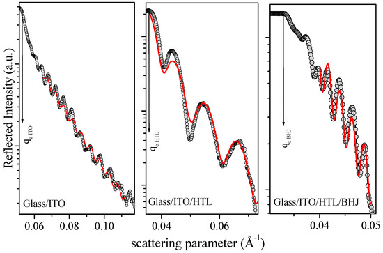
Figure 1.
Reflectivity edges of the various materials, layer by later. Red lines are the Parratt fits used to deduce electron density, as follows: glass/ITO, ρe = 5.6 × 10⁻⁵ Å−2; glass/ITO/ K6-P2W18 ρe = 3.04 × 10⁻⁵ Å−2; glass/ITO/ K6-P2W18/P3HT:PCBM, ρe = 1.3 × 10⁻⁵ Å−2.
Reciprocal space regions, depending on the different position of the critical reflection edges (qc) associated with the materials under investigation, and the reflectivity edges of the various materials, layer by layer, were monitored.
Electron densities were deduced according to the equation relating critical scattering parameter and critical angle qc ≅ αc/λ with (λ being the incident wavelength, ρe the material density and re the classical electron radius [41]): glass/ITO, ρe = 5.6 × 10⁻⁵ Å−2; glass/ITO/ K6-P2W18 ρe = 3.04 × 10⁻⁵ Å−2; glass/ITO/ K6-P2W18/P3HT:PCBM, ρe = 1.3 × 10⁻⁵ Å−2. These values were found to be in excellent agreement with the expected values calculated on the basis of the nominal mass densities of the materials and their composition [30]. Morphological parameters were also deduced and are reported in Table 1 for clarity.

Table 1.
Morphological parameters deduced by the Parratt fitting of patterns in Figure 1.
3.2. In-Situ Time-Resolved Measurements
K6-P2W18 films of different thicknesses were deposited on top of glass only, and in-situ time-resolved ED-XRR measurements were performed under illumination (24 h) to ensure the stability of the material independently of the device architecture. The acquisition time was 20 min, in order to optimize the signal to noise ratio while preserving a reasonable time resolution to detect morphological/electron density degradation occurring as a consequence of light/ temperature induced while the cell was illuminated with a white light lamp (10 mW/cm2).
The results for two films are reported in Figure 2. The ED-XRR patterns are plotted as a function of the scattering parameter and illumination time. Experimental conditions were set to detect both the critical edge (qc)—crucial for electron density determination—and a sufficient number of Kiessig fringes—essential to determine the morphological parameters (film thickness and roughness) [42] by means of the Parratt fitting procedure (red line) [34]. As visible to the naked eye, no degradation occurred upon light exposure, and no variation in the pattern shape (fringes frequency, curve slope or edge position) was detected, as evidenced by arrows connecting the minima of a Kiessig fringe; thus ensuring the possibility to precisely observe the real-time evolution of the system. The morphological parameters remained stable as well as the electron density for both films: (A) d = 120(5) Å and σ = 7(1) Å; (B) d = 515(5) Å and σ = 4(1) Å.
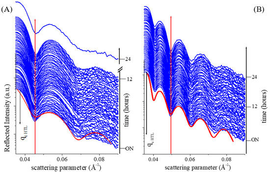
Figure 2.
In situ time resolved morphological and electron density monitoring glass/HTL samples under illumination, representative of different thicknesses (d) taken into account: (A) d = 120Å; (B) d = 515Å. Parratt fit (red line)—used to deduce morphological parameters and electron density—is shown for the first pattern.
The same experimental procedure was followed after depositing the HTL material on top of a glass/ITO, with indium tin oxide being a semiconductor with a wide band gap ( eV), having excellent photo electrolytic properties, and being transparent (80–95%) in the visible range. In the system under investigation, it represents the transparent electrode—of particular interest to high efficiency OPV solar cells. As visible in Figure 3, ITO strongly modifies the overall system: the indium tin oxide reflection edge (qc ITO) affects the ED-XRR patterns—its electron density being much higher than that of HTL. The In adsorption edge is also visible in the figure near 0.065 Å. The monitoring of the real time reflectivity evolution was possible in the same experimental conditions as for the glass/HTL system, and the Parratt fitting (red line) procedure was performed. In Figure 3B, the time evolution of ρe HTL is reported, with no modification occurring. The film thickness d = 520(5) Å and roughness σ = 5(1) Å were also stable.
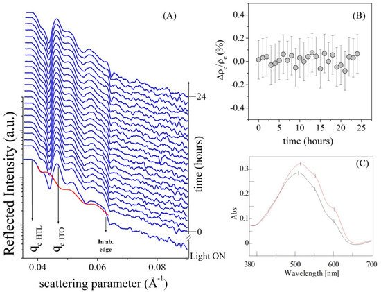
Figure 3.
(A) In-situ time-resolved EDXR patterns of glass/ITO/HTL collected upon prolonged illumination. As visible, despite the presence of ITO reflectivity and absorption edge, HTL signal is still detected and fitted by Parratt model (red line). (B) Electron density monitoring showing no modification. (C) UV-VIS spectra collected prior (red line) and after illumination (black line).
Despite the apparent morphological stability, the UV-Vis absorption measurements (Figure 3C) performed upon the pristine (red line) and illuminated (black line) system demonstrate a slight aging in terms of decreased overall absorption intensity. The absorption bands remain in the same positions, at 513(2) nm, 552(2) nm, and 602(2) nm, respectively.
Since XRR measurements of layered systems enables us to deduce both the surface and buried interface roughness of the system [29], AFM measurements (10 μm × 10 μm) were performed to further characterize the surface texture of the sample before and after illumination. The results shown in Figure 4 are representative of several explored portions of the pristine and aged sample, clearly showing that no surface modification occurred as consequence of prolonged illumination, thus supporting the reflectivity data.
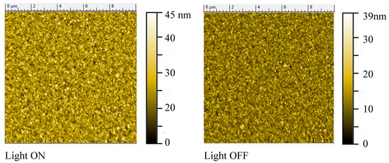
Figure 4.
AFM images—representative of several investigated portions—collected upon the glass/ITO/HTL intermediate sample shown in Figure 3 (d = 520 Å), before and after prolonged illumination, supporting ED-XRR data, proving no morphological modification occurred as a consequence of aging.
The estimated mean surface roughness was σAFM = 5.2(5) nm on the as-deposited sample, and σAFM = 5.0(5) nm for the illuminated sample; the granular texture was preserved.
Subsequently, the BHJ was deposited on top of the HTL. It is well-known that the hole and electron extracting interlayers in the organic solar cells play an important role in high-performing devices, and monitoring their interfacial and superficial morphological/electron density properties is crucial.
Time-resolved ED-XRR patterns were collected in situ for 60 h overall in the previously described experimental conditions. The time evolution of morphological parameters and electron density was obtained, giving an insight into the physical process occurring at the HTL/BHJ interface during illumination. As visible in Figure 5, where the XRR patterns are plotted in linear scale for clarity, with illumination time, oscillations appear at higher q values (labelled in the figure with a dot), and the amplitude is strongly enhanced.
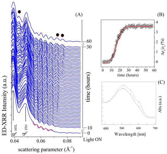
Figure 5.
(A) Sequence of Reflectivity Patterns collected upon the complete system as a function of illumination time and scattering parameter. Strong electron density increase is observed as indicated by the rise of new Kiessig fringes labelled with a black dot. In Figure (B), the electron density percentage increase is shown as deduced by the accurate Parratt fitting of each pattern in (A). A sigmoidal trend (red line) is observed. (C) UV-VIS spectra were collected prior to (red line) and after illumination (black line).
Theoretical modelling of reflectivity patterns attributes the amplitude variation either to a roughness variation or to an electronic density increase. However, roughness modification is strictly entangled to a slope variation of the curves, which is not the present case. The Parratt fitting procedure was performed on all spectra, and no morphological modification was observed (d = 1460(5) Å, σ = 5(1) Å). However, as previously reported [11], after illumination, a strong electron density increase was observed for the HTL material. The fit of the time-resolved experimental data reported in Figure 5A allowed the evolution of ρe to be followed, and the results are reported in Figure 5B. A sigmoidal trend was observed, with 8 h of induction time, and saturation reached after 30 h.
In Figure 5C, UV-Vis absorption spectra of the pristine (red line) and aged (black line) system show moderate aging due to prolonged illumination. The absorption bands are still clearly detected and perfectly overlap those previously measured and reported in Figure 3: 512(2) nm, 553(2) nm, 603(2) nm.
3.3. Photovoltaic Characterization Data
Finally, K6-P2W18 was implemented into a full stack of layers to produce a photovoltaic cell. The results are presented in Figure 6.
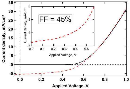
Figure 6.
Current density as a function of the applied bias of an {ITO/K6-P2W18(>45 nm)/P3HT-PCM (120 nm)/LiF(0.7 nm)/Al} solar cell, at 80 mW/cm². The curve corresponding to the I(V) characterization performed in the dark is reported as a black line; the I(V) curve under illumination is plotted as a red dash line. The inset graph is a zoom into the fourth quadrant to highlight the fill factor, measured at 45%.
The graph presented in Figure 6 is characteristic of an I(V) for solar cell under illumination and in the dark. In the absence of light (black line), the device behaves as a Schottky diode. It is blocking at a negative bias and passing at a positive bias. Under illumination, the black curve is shifted in the negative current, demonstrating the photovoltaic effect and the efficiency (at least in terms of electronic building bands) of the device. The shape of the red dash curve in Figure 6 is the proof that K6-P2W18 is acting as an electronic relay from the P3HT:PCBM blend to the ITO for the holes, and from ITO to P3HT:PCBM for the electrons. If not, the curve would likely be a straight line passing through zero (in dark and light analysis) and a bad band adjustment of K6-P2W18, which is not the case.
In this measurement, the efficiency was calculated at almost 3%, with an open circuit voltage of 0.58V and a current density of 8.9 mA/cm².
The presence of the POM at the anodic side adjacent to ITO allows a photocurrent under illumination despite the band misalignment [11], thanks to the presence of the gap state below the Fermi level.
4. Discussion
Degradation effects and aging under ambient conditions/during operation are the main issues to address for a proper improvement in OPV technologies. In these devices, several degradation pathways are present, related to the intrinsic components, to exposure to air/moisture, to heat induced by illumination and light itself, as well as the architecture instability mostly associated with interface aging phenomena.
With these constraints in mind, we have performed an accurate in-situ time-resolved investigation of the morphological and optical stability of a polyoxometalate film by means of ED-XRR, AFM, and UV-Vis spectroscopy.
We have demonstrated the stability of the K6-P2W18 films, independent of their thickness; UV-Vis measurements showed that the material presented a slight decrease in the overall absorption after 24 h of exposure. However, despite the light/material interaction, film thickness, roughness and electron density were preserved.
Subsequently, the polyoxometalate film was deposited on top of the transparent glass/ITO electrode, the in-situ time-resolved ED-XRR technique allowed the morphological and electron density to be accurately monitored. The K6-P2W18 film retained its previously described characteristics.
Finally, the BHJ was deposited on top of the structure and the complete system was illuminated for 60 h, and promising behaviour for further OPV implementation was observed: the POM film as well as the BHJ were morphologically stable. No increase in roughness was observed, indicating interface stability. Interestingly, it was possible to monitor the HTL/BHJ interface electron density evolution over time during illumination, and an increase of 3.5% was observed.
Therefore, this phenomenon can be directly related to the electronic processes in the OPV structure. Indeed, under illumination, an exciton is generated in the P semiconductor, and is separated into two free charges due to the internal field at the P/N junction of the solar cell.
In this article, we have demonstrated that the POM acts as an electronic relay. The appearance of a photocurrent under illumination implies that charges are driven across the POM layer: electrons migrate from the ITO to the P3HT-PCBM, and holes are driven from the P3HT-PCBM to the ITO (to conserve the electrical neutrality).
In samples measured by ED-XRR, the ITO is grounded, whereas the P3HT:PCBM is not connected so the circuit is not closed. It is not a full device, but only half of it. As a result, the charges provided by the ITO are trapped, whereas they are collected by the POM material at the POM/P3HT:PCBM interface.
5. Conclusions
In conclusion, the combination of the photovoltaic measurements and ED-XRR observations indicate two major conclusions regarding the electronic process in which the K6-P2W18 is involved. First, as an interlayer, K6-P2W18 can drive holes from P3HT:PCBM to ITO; this is counter-intuitive, because POM are known as N-type semiconductors. The second conclusion comes from the increase in the density of electrons at the POM/active layer interface. Indeed, this fact proves that electrons cannot be driven from the P3HT:PCBM layer to ITO. The K6-P2W18 is thus hole sensitive and selective, despite its N-type behaviour. That also proves the electronic bridging of the solar cell at the anodic side was well constructed. Moreover, great stability for the polyoxometalate layer was observed upon illumination, retaining its ability as a hole transporting layer for more than 30 h. UV-Vis spectroscopy supported this indication—the overall loss of light absorbance capability being very limited after such a prolonged illumination.
Due to the combination of the homemade set-up (ED-XRR + AFM, + light) and the K6-P2W18O62, we have demonstrated that the high reproducibility of measurements allows following aging processes over several hours. These experimental ED-XRR observations of the HTL stability in working conditions are promising indications for the further implementation of the glass/ITO/ K6-P2W18/PH3T:PCBM into a complete OPV device.
Author Contributions
Conceptualization, B.P.; methodology, A.G. and B.P.; formal analysis, A.G. and B.P.; software: M.G.; investigation: POM synthesis, Q.Z.; AFM experiments, M.G. and A.G.; EDXR experiments, A.G.; UV-VIS experiments, M.G.; data curation, A.G.; writing—original draft preparation, A.G. and B.P.; writing—review and editing on synthesis material and/or OPV statements, A.P., L.T. and N.T.B.; supervision, B.P.; PhD supervision, A.P., N.T.B. and L.T.; All authors have read and agreed to the published version of the manuscript.
Funding
The authors would like to thank the région Ile de France and the DIM Nano-K for funding the PhD grant to Qirong Zhu.
Acknowledgments
The authors are grateful to Guillaume Izzet for stimulating discussions and for his precious advice regarding the POMs synthesis.
Conflicts of Interest
The authors declare no conflict of interest.
References
- Cao, Q.; Kim, H.S.; Pimparkar, N.; Kulkarni, J.P.; Wang, C.; Shim, M.; Roy, K.; Alam, M.A.; Rogers, J.A. Medium-scale carbon nanotube thin-film integrated circuits on flexible plastic substrates. Nature 2008, 454, 495–500. [Google Scholar] [CrossRef]
- Ulanski, J.; Luszczynska, B.; Matyjaszewski, K. (Eds.) Solution-Processable Components for Organic Electronic Devices; Wiley-VCH: Weinheim, Germany, 2019. [Google Scholar]
- Lee, C.K.; Seo, J.G.; Kim, H.J.; Hong, S.J.; Song, G.; Ahn, C.; Lee, D.J.; Song, S.H. Versatile and Tunable Electrical Properties of Doped Nonoxidized Graphene Using Alkali Metal Chlorides. ACS Appl. Mater. Interfaces 2019, 11, 42520–42527. [Google Scholar] [CrossRef]
- Hammond, S.R.; Meyer, J.; Widjonarko, N.E.; Ndione, P.F.; Sigdel, A.K.; Garcia, A.; Miedaner, A.; Lloyd, M.T.; Kahn, A.; Ginley, D.S.; et al. Low-temperature, solution-processed molybdenum oxide hole-collection layer for organic photovoltaics. J. Mater. Chem. 2012, 22, 3249–3254. [Google Scholar] [CrossRef]
- Hösel, M.; Angmo, D.; Krebs, F.C. Handbook of Organic Materials for Optical and (Opto)Electronic Devices: Properties and Applications; Series in Electronic and Optical Materials; Woodhead Publishing: Sawston/Cambridge, UK, 2013; pp. 473–507. [Google Scholar]
- Available online: www.nrel.gov/pv/cell-efficiency.html (accessed on 3 July 2020).
- Zhan, L.; Li, S.; Lau, T.-K.; Cui, Y.; Lu, X.; Shi, M.; Li, C.-Z.; Li, H.; Hou, J.; Chen, H. Over 17% efficiency ternary organic solar cells enabled by two non-fullerene acceptors working in an alloy-like model. Energy Environ. Sci. 2020, 13, 635–645. [Google Scholar] [CrossRef]
- Basu, P.K.; Kumbhar, S.; Sreejith, K.P.; Yadav, T.S.; Kottantharayil, A.; Arora, B.M.; Narasimhan, K.L.; Sharma, A.K. Active area cell efficiency (19%) monocrystalline silicon solar cell fabrication using low-cost processing with small footprint laboratory tools. Bull. Mater. Sci. 2019, 42, 33. [Google Scholar] [CrossRef]
- Lucera, L.; Machui, F.; Kubis, P.; Schmidt, H.D.; Adams, J.; Strohm, S.; Ahmad, T.; Forberich, K.; Egelhaaf, H.-J.; Brabec, C.J. Highly efficient, large area, roll coated flexible and rigid OPV modules with geometric fill factors up to 98.5% processed with commercially available materials. Energy Environ. Sci. 2016, 9, 89–94. [Google Scholar]
- Taroni, P.J.; Hoces, I.; Stingelin, N.; Heeney, M.; Bilotti, E. Thermoelectric Materials: A Brief Historical Survey from Metal Junctions and Inorganic Semiconductors to Organic Polymers. IJC: Org. Electron. 2014, 54, 534–552. [Google Scholar]
- Zhu, Q.; Paci, B.; Generosi, A.; Renaudineau, S.; Gouzerh, P.; Liang, X.; Mathieu, C.; Rountree, C.; Izzet, G.; Proust, A.; et al. Conductivity via Thermally Induced Gap State in a Polyoxometalate Thin Layer. J. Phys. Chem. C 2019, 123, 1922–1930. [Google Scholar] [CrossRef]
- Pope, M.T.; Müller, A. Polyoxometalate Chemistry: An Old Field with New Dimensions in Several Disciplines. Angew. Chem. Int. Ed. Engl. 1991, 30, 34–48. [Google Scholar] [CrossRef]
- Sadakane, M.; Steckhan, E. Electrochemical Properties of Polyoxometalates as Electrocatalysts. Chem. Rev. 1998, 98, 219–238. [Google Scholar] [CrossRef]
- Papaconstantinou, E. Photochemistry of Polyoxometallates of Molybdenum and Tungsten and/or Vanadium. Chem. Soc. Rev. 1989, 18, 1–31. [Google Scholar] [CrossRef]
- Gómez-Romero, P. Polyoxometalates as photoelectrochemical models for quantum-sized colloidal semiconducting oxides. Solid State Ion. 1997, 101, 243–248. [Google Scholar] [CrossRef]
- Busche, C.; Vilà-Nadal, L.; Yan, J.; Miras, H.N.; Long, D.-L.; Georgiev, V.P.; Asenov, A.; Pedersen, R.H.; Gadegaard, N.; Mirza, M.M.; et al. Design and Fabrication of Memory Devices Based on Nanoscale Polyoxometalate Clusters. Nature 2014, 515, 545–549. [Google Scholar] [CrossRef] [PubMed]
- Vasilopoulou, M.; Polydorou, E.; Douvas, A.M.; Palilis, L.C.; Kennou, S.; Argitis, P. Annealing-Free Highly Crystalline Solution-Processed Molecular Metal Oxides for Efficient Single-Junction and Tandem Polymer Solar Cells. Energy Environ. Sci. 2015, 8, 2448–2463. [Google Scholar] [CrossRef]
- Jeevanandam, J.; Barhoum, A.; Chan, Y.S.; Dufresne, A.; Danquah, M.K. Review on nanoparticles and nanostructured materials: History, sources, toxicity and regulations. Beilstein J. Nanotechnol. 2018, 9, 1050–1074. [Google Scholar] [CrossRef] [PubMed]
- Chen, W.; Nikiforov, M.P.; Darling, S.B. Morphology characterization in organic and hybrid solar cells. Energy Environ. Sci. 2012, 5, 8045–8074. [Google Scholar] [CrossRef]
- Paci, B.; Generosi, A.; Rossi Albertini, V.; Perfetti, P.; de Bettignies, R. The Role of C60 Barrier Layer in Improving the Performances of Efficient Polymer-Based Photovoltaic Devices: An AFM/EDXR Time-Resolved Study. J. Phys. Chem. C 2009, 113, 19740–19747. [Google Scholar] [CrossRef]
- Paci, B.; Generosi, A.; Rossi Albertini, V.; Perfetti, P.; de Bettignies, R.; Sentein, C. Photo-degradation and stabilization effects in operating organic photovoltaic devices by joint photo-current and morphological monitoring. Solar Energy Mater. Solar Cells 2008, 92, 799–804. [Google Scholar] [CrossRef]
- Guerrero, A.; Garcia-Belmonte, G. Recent Advances to Understand Morphology Stability of Organic Photovoltaics. Nano-Micro Lett. 2017, 9, 10. [Google Scholar] [CrossRef]
- McEvoy, A.; Castaner, L.; Markvart, T. (Eds.) Solar Cells: Materials, Manufacture and Operation, 2nd ed.; Academic Press: Cambridge, MA, USA, 2012. [Google Scholar]
- Felici, R. On the use of energy dispersive X-ray reflection to study the electronic density profile at surfaces and interfaces. Rigaku J. 1995, 12, 11–17. [Google Scholar]
- Daillant, J.; Gibaud, A. (Eds.) X-ray and Neutron Reflectivity Principles and Applications, 1st ed.; Springer: Berlin, Germany, 1999. [Google Scholar]
- Tanner, B.K. Grazing incidence X-ray reflectivity and scattering. In Handbook of Advanced Non-Destructive Evaluation; Ida, N., Meyendorf, N., Eds.; Springer: Cham, Switzerland, 2018. [Google Scholar]
- Chebil, S.M.; Vignaud, G.; Grohens, Y.; Konovalov, O.; Sanyal, M.K.; Beuvier, T.; Gibaud, A. In Situ X-ray Reflectivity Study of Polystyrene Ultrathin Films Swollen in Carbon Dioxide. Macromolecules 2012, 45, 6611–6617. [Google Scholar] [CrossRef]
- Orita, K.; Morimura, T.; Horiuchi, T.; Matsushige, K. In situ energy-dispersive X-ray reflectivity measurements of structural changes in thin films for organic electroluminescent devices. Synth. Met. 1997, 91, 155–158. [Google Scholar] [CrossRef]
- Rossi Albertini, V.; Paci, B.; Generosi, A. Energy dispersive X-ray reflectometry as a unique laboratory tool for investigating morphological properties of layered systems and devices. J. Phys. D Appl. Phys. 2006, 39, 461–486. [Google Scholar] [CrossRef]
- Generosi, A.; Rossi Albertini, V.; Rossi, G.; Paoletti, A.M.; Caminiti, R. Energy dispersive X-ray reflectometry of the NO2 interaction with ruthenium phthalocyanine films. J. Phys. Chem. B 2003, 107, 575–579. [Google Scholar] [CrossRef]
- Generosi, A.; Paci, B.; Rossi Albertini, V.; Perfetti, P.; de Bettignies, R.; Firon, M.; Leroy, J.; Sentein, C. In situ energy dispersive X-ray reflectometry measurements on organic solar cells upon working. Appl. Phys. Lett. 2005, 87, 194110–194112. [Google Scholar]
- Paci, B.; Generosi, A.; Rossi Albertini, V.; Spyropoulos, G.D.; Stratakis, E.; Kymakis, E. Enhancement of photo/thermal stability of organic bulk heterojunction photovoltaic devices via gold nanoparticles doping of the active layer. Nanoscale 2012, 4, 7452–7459. [Google Scholar] [CrossRef]
- Paci, B.; Generosi, A.; Rossi Albertini, V.; Perfetti, P.; de Bettignies, R.; Sentein, C. Time resolved morphological study of organic thin film solar cells based on calcium/aluminum cathode material. Chem. Phys. Lett. 2008, 461, 77–81. [Google Scholar] [CrossRef]
- Chason, E.; Mayer, T.M. Thin film and surface characterization by specular X-ray reflectivity. Crit. Rev. Solid State Mater. Sci. 1997, 22, 1–67. [Google Scholar] [CrossRef]
- Bontempi, E.; Depero, L.E.; Bergese, P. A simple solution to systematic errors in density determination by X-ray reflectivity: The XRR-density evaluation (XRR-DE). Appl. Surf. Sci. 2006, 253, 28–32. [Google Scholar]
- Neuhold, A.; Brandner, H.; Ausserlechner, S.J.; Lorbek, S.; Neuschitzer, M.; Zojer, E.; Teichert, C.; Resel, R. X-ray based tools for the investigation of buried interfaces in organic electronic devices. Org. Electron. 2013, 14, 479–487. [Google Scholar] [CrossRef]
- Sakurai, K. Exploring surfaces and buried interfaces of functional materials by advanced X-ray and neutron techniques. J. Phys. Condens. Matter 2010, 22, 470301. [Google Scholar] [CrossRef] [PubMed]
- Kakavelakis, G.; Paradisanos, I.; Paci, B.; Generosi, A.; Papachatzakis, M.; Maksudov, T.; Del Rio Castillo, A.E.; Najafi, L.; Kioseoglou, G.; Stratakis, E.; et al. Large area-ambient stable Perovskite Solar Cells using MoS2 as hole transport interlayer. Adv. Energy Mater. 2018, 8, 170228. [Google Scholar]
- Paci, B.; Generosi, A.; Generosi, R.; Bailo, D.; Rossi Albertini, V. Joint time-resolved AFM/EDXR techniques for thin films morphological in situ studies. Chem. Phys. Lett. 2009, 483, 159–163. [Google Scholar] [CrossRef]
- Parratt, L.G. Surface Studies of Solids by Total Reflection of X-rays. Phys. Rev. 1954, 95, 359–369. [Google Scholar] [CrossRef]
- Ballirano, P.; Caminiti, R. Rietveld refinement on laboratory energy dispersive X-ray diffraction (EDXD) data. J. Appl. Crystallogr. 2001, 34, 757–762. [Google Scholar] [CrossRef]
- Fujii, Y. Analysis of surface roughness correlation function by X-ray reflectivity. Surf. Interface Anal. 2016, 48, 1136–1138. [Google Scholar] [CrossRef]
© 2020 by the authors. Licensee MDPI, Basel, Switzerland. This article is an open access article distributed under the terms and conditions of the Creative Commons Attribution (CC BY) license (http://creativecommons.org/licenses/by/4.0/).