1. Introduction
ZnO-based materials have attracted a lot of intensive research in recent decades due to their interesting material properties and wild applications. It is well known that they are abundant, non-toxic and low-cost semiconductors with a wide band gap and large exciton binding energy. They also exhibit piezoelectric and pyroelectric properties and a large number of nanostructures. By virtue of these advantages, various kinds of optoelectronic devices, such as thin-film transistors (TFTs) [
1], solar cells [
2], ultraviolet (UV) lasers [
3], photodetectors [
4], and surface acoustic wave (SAW) sensors [
5] have been developed. For example, due to their large band gap energy (above 3.37 eV) and good electrical properties (high electron mobility and low resistance), ZnO-based materials have the great benefit to be applied in large-area TFT-LCD panels or transparent electronic circuits to increase the transparency. Because of the good optoelectronic properties in the near-UV range and their excellent chemical and thermal stabilities, they are promising materials for the next generation of short-wavelength light emitting diode (LED) and laser diodes [
6]. Among ZnO-based materials, ZnMgO is a strong candidate for UV photodetectors due to its high absorption coefficient, tunable band gap energy (3.3–7.8 eV), and high radiation hardness [
7,
8]. Furthermore, various kinds of nanostructured ZnO-based materials, including nanodots, nanorods, nanowires and nanobelts have been realized by different methods and unambiguously demonstrate that they are probably the richest family of nanostructures among all materials [
9]. Enhanced photoresponse for photodetectors and high sensitivity for high-precision pH sensors have been demonstrated using ZnO and ZnMgO nanorod arrays [
10,
11,
12]. These unique nanostructures, not only possess high surface area and good photoresponsivity for optical detectors and gas sensing applications, but they also show biocompatibility, biomimetic, and high electron communication features, leading to a wide range of applications in biosensors [
13]. The surface effects on physical properties of ZnO nanostructures have demonstrated that the high surface-to-volume (S/V) ratio significantly improved the gas/chemical sensing sensitivity and imposed the challenges for biosensing applications. There are many remarkable ZnO-based devices that have been developed and used in commercial fields, such as telecommunications, air quality monitoring, high-temperature flame detection, optical imaging, and optoelectronic devices [
14,
15]. In order to achieve device miniaturization and reducing the cost of mass production, a great deal of effort has been focused on synthesis and characterization. There are a number of methods that have been developed for the growth of ZnO-based films, including metalorganic chemical vapor deposition (MOCVD) [
16], magnetron sputtering [
17,
18], molecular beam epitaxy (MBE) [
19], atomic layer deposition (ALD) [
20], the sol–gel method [
21,
22,
23], and spray pyrolysis method [
24]. Among these methods, the sol–gel process is a cost-effective technique and has been widely used to synthesize metal-oxide thin films, organic–inorganic hybrids, nanoparticles and nanostructures. Compared to other crystal synthesis methods, it has advantages such as lower process temperatures, higher homogeneity and purity, easy control of different doping amounts, and the ability to synthesize multicomponent compositions. In this paper we used the sol–gel method to grow Zn
1−xMg
xO (x = 0, 0.03, 0.05, and 0.07) films with a uniform thickness and smooth morphology on silicon substrates. We tried to understand the effect of the incorporation of Mg on their optical properties, such as band gap energy and UV response. We found that the band gap energy increased with increasing Mg content, but the UV response did not improve by the incorporation of Mg. Because the UV response is an important characteristic for UV photodetectors, we applied the hydrothermal method to grow Zn
1−xMg
xO nanorod arrays on a ZnO seed layer to enhance the UV light response. From these results, we found that nanorod arrays are a useful method to improve the UV light response. Furthermore, the microstructures and surface morphologies of the Zn
1−xMg
xO films and nanorod arrays were measured by XRD and FE-SEM, respectively.
2. Materials and Methods
The source materials for the growth of Zn1−xMgxO (x = 0, 0.03, 0.05, and 0.07) films were prepared with the precursors of zinc acetate dehydrate (CH3COO)2Zn·2H2O and (CH3COO)2Mg·4H2O. We used 2-Methoxyethanol as solvent to keep the concentration of metal ions at 0.05 M, with magnesium mole ratios of 0%, 3%, 5%, and 7%, respectively. We also added ethanolamine into the solution to obtain a stable precursor solution. After stirring at room temperature (300 K) for 3 h using a magnetic stirrer and letting the solution sit for 72 h, a transparent solution was obtained for the growth of Zn1−xMgxO films. We used n-type silicon wafers (resistance of 0.55–1.2 Ω) as substrates. A typical ultrasonic cleaning process with acetone and ethanol was used to remove possible contamination and particles; after that, the substrates were rinsed in deionized (DI) water and dried by nitrogen gas. Each layer was fabricated by dropping the sol–gel solution on the substrates which were mounted on a spin coater rotating in two steps: the first step was a spinning rate of 1000 rpm for 10 s and the second step was 3000 rpm for 30 s. After that, the samples were heated at 300 °C for 2 min to evaporate the solvent. We repeated the process ten times to grow the Zn1−xMgxO films. The last process was annealing the films at 600 °C for 6 h in a rapid thermal annealing (RTA) system. In order to enhance the UV light response, we grew the nanorods on silicon substrates with two layers of ZnO nanofilms as a seed layer using the hydrothermal method. We used hexamethylenetetramine as solvent and diluted with DI water to keep the concentration of metal ions at 0.02 M, with magnesium mole ratios of 0%, 3%, 5%, and 7%, respectively. The ZnO seed layer film was dipped into this solution for one hour and the temperature kept at 90 °C to grow the Zn1−xMgxO nanorod arrays.
The crystal microstructures of all the Zn1−xMgxO films and nanorod arrays were examined using an X-ray diffractometer (Rigaku D/max-2200) with CuKα radiation. The surface morphologies and cross-section images were analyzed using a cold-field emission scanning electron microscope (FE-SEM, Hitachis-4800) at 3.0 kV. A UV-VIS-NIR absorption spectrometer (Jasco V-670) was used to investigate the band gap energies of the Zn1−xMgxO films. For understanding the UV light response of all Zn1−xMgxO films and nanorod arrays, a Keithley 2400 sourcemeter equipped with a UV lamp (254 nm) was used to perform the current–voltage (I–V) measurements in the voltage range between −5 V and to 5 V under dark and UV illuminated conditions.
3. Results and Discussion
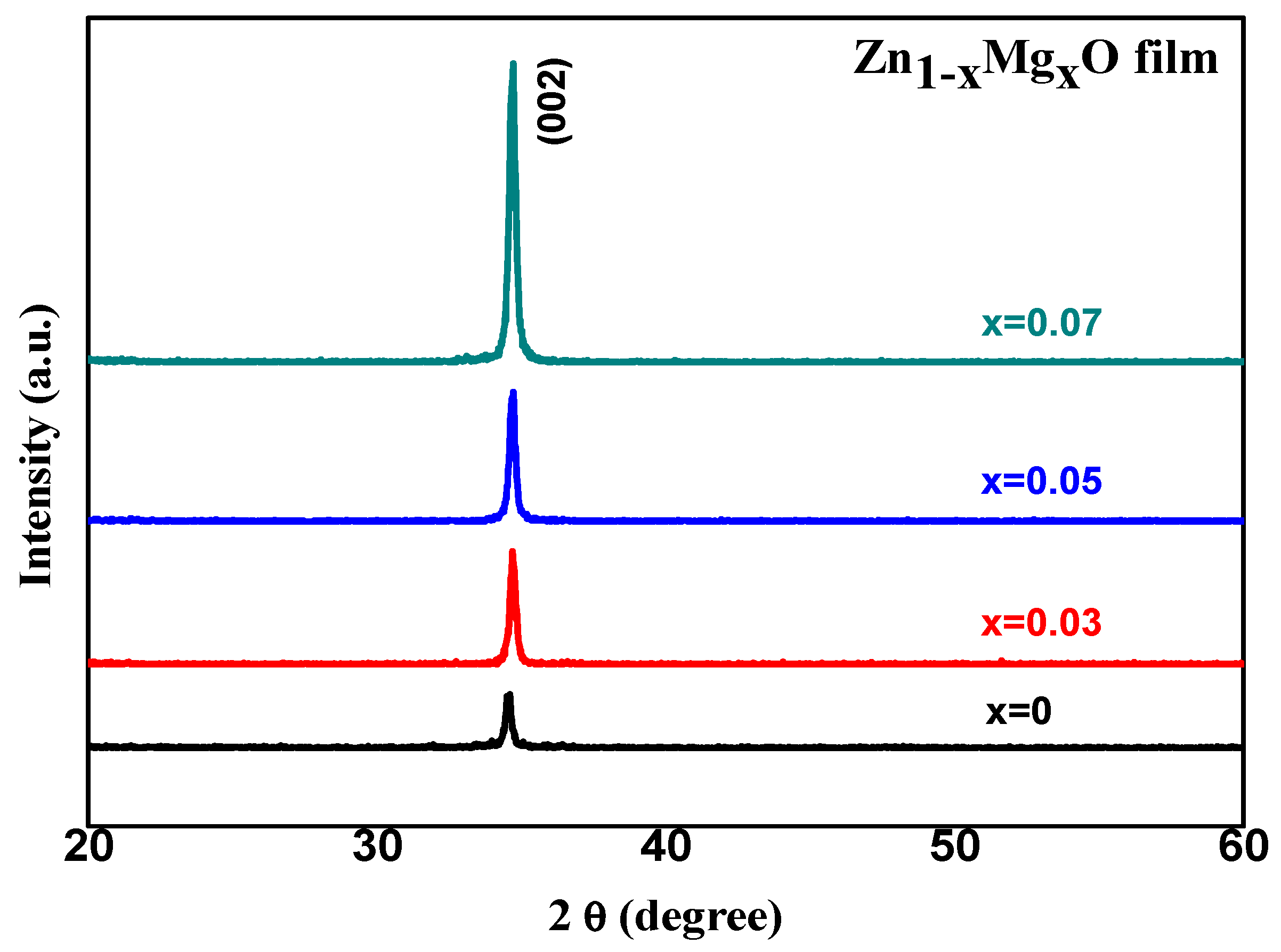
Figure 1 shows the XRD patterns of the Zn
1−xMg
xO (x = 0, 0.03, 0.05, and 0.07) films grown on silicon substrates. We found only one main peak located at
degree for undoped ZnO (x = 0) and it shifted toward 34.71 degree for x = 0.07, which indicated that all the Zn
1−xMg
xO films had a c-axis preferential orientation. It can be seen that the intensity of these peaks gradually increased as the Mg content increased, which indicates the enhancement of the crystallinity of the films. In addition, all Zn
1−xMg
xO films had the same wurtzite hexagonal crystal structure with the space group P63/mc (JCPDS 36-1451). The lattice constant of the c-axis can be calculated using Equation (1) [
25].
where
h,
k,
l are Miller indices and
a,
c are in plane and vertical lattice parameters, respectively, and
d is the distance between two adjacent planes with the same set of Miller indices. The lattice constant of c-axis can be determined to be 5.1941 Å for x = 0 and decreases to 5.1695 Å for x = 0.07. This result may be understood by the fact that Mg ions incorporated into the ZnO lattice and substituted Zn ions because the ionic radii of
(0.72 Å) is smaller than that of
(0.74 Å) [
26]. This result is similar to the report of Mg-doped ZnO thin films prepared by a modified Pechini method, even though they are polycrystalline films.
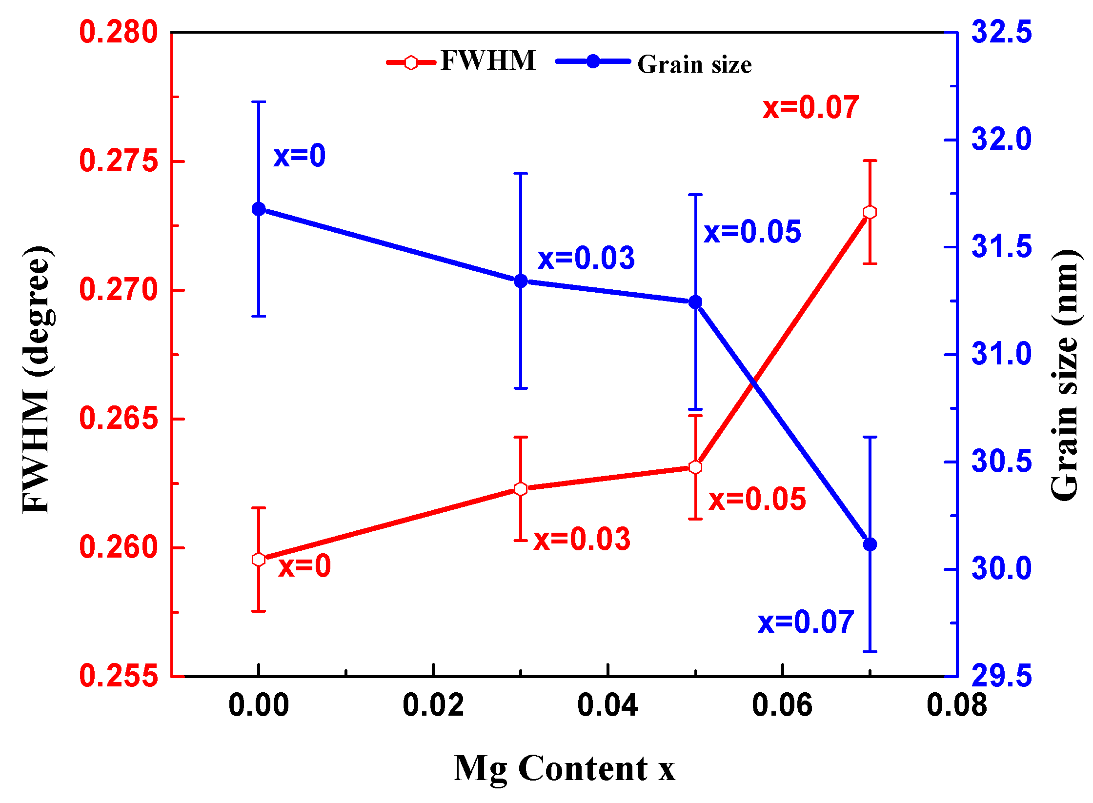
The full width at half maximum (FWHM) values extracted from the XRD (002) peaks and the average grain sizes as a function of Mg content are presented in
Figure 2. The average grain size can be extracted using the Debey-Scherrer formula [
25], D = kλ/βcosθ, where k is the Scherrer constant (k = 0.9), λ is the wavelength of the X-ray radiation, β is the FWHM in radians, and θ is the Bragg diffraction angle. The calculated average grain sizes results are 31.68, 31.34, 31.25, and 30.12 nm, for x = 0, 0.03, 0.05, 0.07, respectively. The grain size determined by the Debey-Scherrer formula is usually smaller than the size observed from their SEM images. Using SEM, one can see physical grain or particle images that may contain several crystalline domains and imperfect regions around the borders between grains. With XRD, the information about the gain size only comes from coherently scattering in the same diffracting volumes. The uncertainty around 0.5 nm is due to the uncertainty of peak position, FWHM, and angle resolution, but this approximation method still gives a reasonable reference. The average grain size decreases with Mg content which is likely due to the Mg-substitution resulting in a local lattice distortion and the formation of a small Mg doped ZnO nanoparticles. The similar results have been reported in manganese (Mn) and iron (Fe) doped ZnO by other investigators [
27,
28].
The surface morphologies and cross-sectional views of Zn
1−xMg
xO films have been investigated using FE-SEM. The results are shown in
Figure 3a,e for x = 0,
Figure 3b,f for x = 0.03,
Figure 3c,g for x = 0.05, and
Figure 3d,h for x = 0.07, respectively. The cross-sectional images
Figure 3e–h present a uniform thickness with a small increase from 181 to 214 nm for increasing Mg content x from 0 to 0.07. The increasing thickness may be responsible for the increase of the XRD (002) peaks intensity for high doping Zn
1−xMg
xO films. The top view images
Figure 3a–d reveal uniform granular surfaces for all films. The grain numbers included in the upper half of the SEM images, as shown by the red squares in
Figure 3, were counted to be around 280, 290, 300, and 310, and the diameter of each grain was estimated to get the averaged grain size, which decreased a little bit from 50 to 47 nm for x = 0 to 0.07. This 3-nm difference of grain size observed in SEM images is not obvious, but still gives a consistent trend with the XRD results.
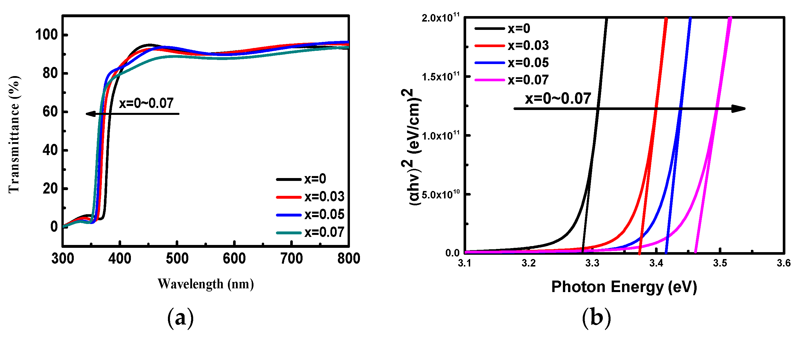
In order to understand the Mg doping effect on the optical band gap energy, the optical transmittance spectra of Zn
1−xMg
xO films have been performed by using a UV-vis absorption spectrometer. Each spectrum was measured twice to check its repeatability. We found that each of the spectra measured at the second time matched well with the first one in a wavelength error below 0.2 nm (about 2 meV for the band gap energy of 3.28 eV).
Figure 4a presents the optical transmittance spectra in the wavelength range of 300–800 nm. In the visible wavelength range from 400 to 700 nm, the spectra show the films are highly transparent with a high transmittance up to 90%. In the short wavelength region below 400 nm, a strong absorbance is observed. It is obvious to find that the cut-off wavelength with an intensive decrease in transmittance shifts toward short wavelength with the increase of Mg-doping concentration. This result implies the absorption edge of Zn
1−xMg
xO films shifts towards high photon energy direction (blue shift).
From the transmittance spectra, absorption coefficient (
α) can be calculated following Bouguer-Lambert-Beer absorption law
α = (1/
t)ln(1/
T), where
t is the thickness of Zn
1−xMg
xO films and
T are the optical transmittance data in function of photon energy [
29]. The
α over the threshold of fundamental absorption obeyed a relationship
αhυ =
A(hυ −
Eg)n, where
A is a function of refractive index and hole/electron effective masses,
h is the Planck’s constant,
v is the photon frequency,
Eg is the band gap energy, and
n = 1/2 for direct band gap semiconductor. On the basis of the Tauc model in the high absorbance region, the optical band gap energy can be calculated using the intercept of
( versus photon energy (
h) plot as shown in
Figure 4b. The calculated band gap energies of Zn
1−xMg
xO films are 3.28, 3.36, 3.41, and 3.46 eV, respectively, for x = 0 to 0.07. This result indicates that with increasing concentration of the dopant, there is a slight increase in the band gap energy. This behavior may be explained by several mechanisms such as (1) the Moss-Burstein band filling effect which originates from the lifting of Fermi level into the conduction band and usually observed in degenerate semiconductors with carrier concentration higher than 10
19 cm
−3; (2) quantum size effect (QSE) which is highly pronounced only when the crystallite size is comparable to its Bohr exciton radius; and (3) the fact that MgO has a wider band gap energy (7.7 eV) than ZnO (3.2 eV). Since our samples were not degenerate n-type semiconductors and their grain sizes calculated from XRD data and SEM images were far beyond the quantum confinement regime, we believe that the shift in absorption edge and widening of the band gap can be attributed to the compositional incorporation and local strain in Zn
1−xMg
xO samples [
30].
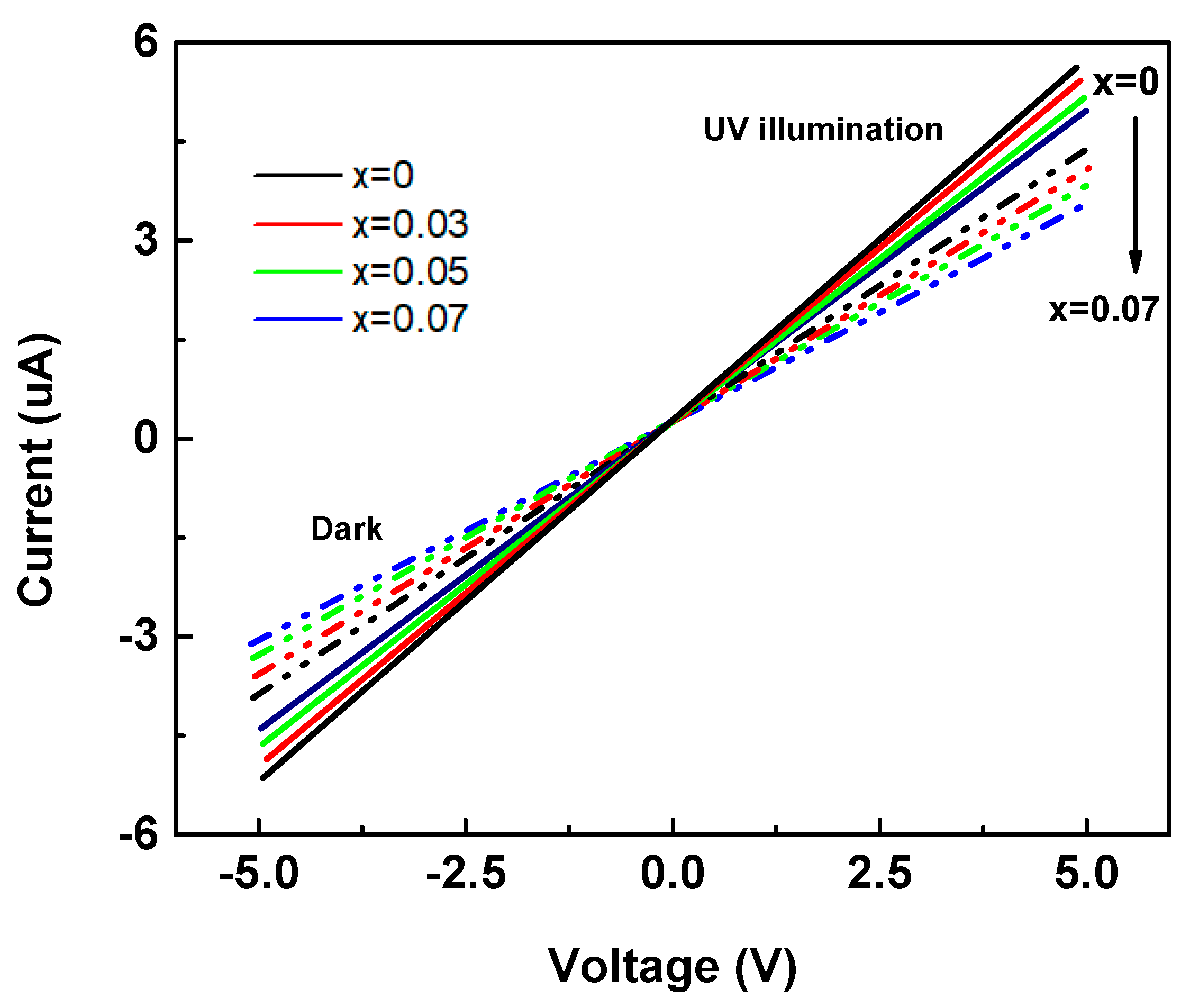
The I–V characteristics of Zn
1−xMg
xO films were measured separately under dark (dark current,
Idark) and UV illumination (photocurrent,
Iphoto) between applied bias range +5 V and −5 V, as shown in
Figure 5. The measured dark currents (
Idark) were 4.21, 4.12, 4.02, and 3.80 μA while the UV illumination current (
Iphoto) were 5.86, 5.52, 5.12, and 4.84 μA (at +5 V bias) for Zn
1−xMg
xO films with x = 0 to 0.07, respectively. For photodetector applications, the UV response can be evaluated by the ratio of photo-to-dark-current (R
CV) defined as (
Iphoto −
Idark)/
Idark. The measurement data and calculation results are listed in
Table 1. The UV response for the Zn
1−xMg
xO films with different Mg contents is in the same order and about two times that of the UV response reported by Tsay et al. [
31].
In this study, we have grown Zn
1−xMg
xO nanorod arrays on pure n-type ZnO seed layer by hydrothermal method to enhance the UV light response.
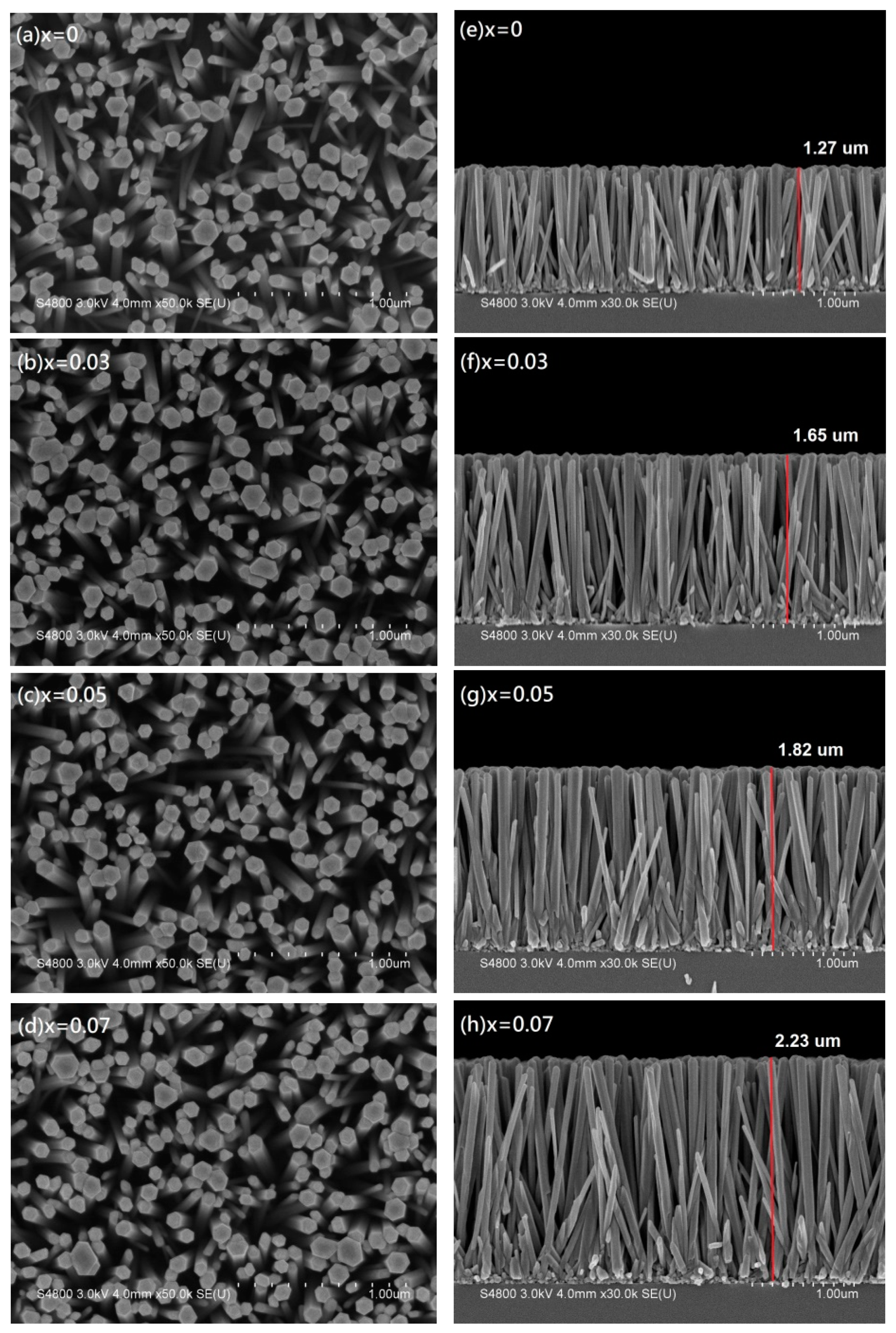
Figure 6 shows top-view and cross-sectional FE-SEM images of Zn
1−xMg
xO nanorod arrays. From the top-view images in
Figure 6a–d, Zn
1−xMg
xO nanorod arrays have clearly hexagonal structure almost along the full length and good uniformity with diameters in the range between 50 to 110 nm. The cross-sectional images in
Figure 6e–h show that well-aligned Zn
1−xMg
xO nanorod arrays were grown preferentially in the vertical direction, which had the same result as the XRD patterns with a c-axis preferential orientation. In addition, it can be observed from the cross-sectional view that when the Mg content x increases from 0 to 0.07, the length of the nanorod arrays increases from 1.27 to 2.23 μm. This result suggested that, compared with the pure ZnO nanorod arrays (x = 0), with increasing Mg content, the growth rate along the c-axis has been improved obviously.
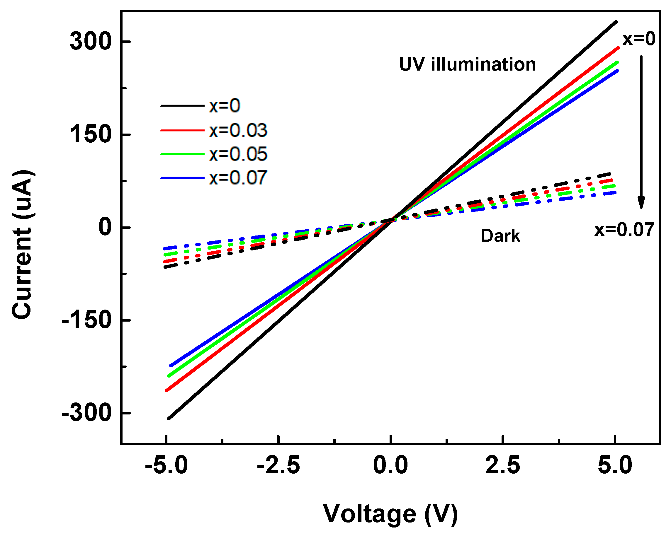
We measured the dark and UV illuminated I–V characteristics of Zn
1−xMg
xO nanorod arrays between applied bias range +5 V and −5 V. The results are presented in
Figure 7 dotted line for dark and solid line for UV illumination. The measured dark currents (
Idark) were 72.5, 69.6, 61.6, and 58.7 μA while the UV illumination current (
Iphoto) were 326, 283, 239, and 216 μA (at +5 V bias) for Zn
1−xMg
xO nanorod arrays with x = 0 to 0.07, respectively. These data and calculated values of (
Iphoto −
Idark)/
Idark are also collected in
Table 1. It is worth mentioning that the nanorod arrays structures highly enhance the UV response about ten times (from 27 to 287 for x = 0.05). We observed that the increase of Mg content did not continue improving the UV response, but the change in structure from films to nanorod arrays resulted in a great improvement in the UV response. We believe the nanorod arrays increased the efficiency of adsorption of incident light that struck on the nanorod arrays because multiple reflections created by the nanorod arrays. It can be imagined that as a ray of light struck a nanorod, a part of it may be reflected from the nanorod array’s surface following Snell’s Law, and the reflected light could easily be incident on another. Each nanorod acts as a light scattering center and enhances the multiple scattering for the UV light [
32].


