1. Introduction
Microwave photonic microcircuits are widely used in applications such as recognition and sensing, optical signal processing, biophotonics, telecommunication networks, and high-speed computing. One of the main drivers for the development of microwave photonics is the telecommunications market. The rapid global spread of wearable devices with wireless Internet access, in addition to the development and implementation of 4G and 5G mobile networks, expansion of video hosting systems, and the Internet of Things (IoT), are exponentially increasing network traffic [
1,
2]. The transfer between users of an increasing volume of data, which is uploaded and downloaded on remote servers in data centers, is the main primary source of load on fiber-optic telecommunication lines.
The equipment of dense wavelength division multiplexing (DWDM) communication systems is used to provide the bandwidth of the communication lines. The development of this equipment requires a corresponding component base. An electro-optical Mach–Zehnder modulator (MZM) is one of the key elements in microwave photonics. In the development of integrated optoelectronic devices, InP is one of the basic materials that makes it possible to create both active and passive elements [
3].
In general, the InP-based MZM manufacturing process includes the following technological blocks: formation of optical waveguides, mesa isolation (optional), p- and n-ohmic contacts, surface planarization (optional), interconnections, dividing a semiconductor wafer into single dies, and deposition of an antireflection (AR) coating on the ends of the dies. Many research groups have developed their own manufacturing processes for InP-based MZMs [
4,
5,
6,
7,
8,
9,
10,
11,
12,
13,
14,
15,
16,
17,
18], and a number of manufacturers have industrialized the production of InP-based MZMs [
4,
5,
6,
12]. Nevertheless, development and optimization of the manufacturing technology of these devices continues.
The technological process presented by the Cobra research institute uses n
+ InP wafers with a p-i-n heterostructure formed on their surface [
4,
5]. The formation of waveguide structures is performed using a combination of wet and dry etching methods. The top highly doped p-layer of the heterostructure is removed to form an isolation between the active elements. The surface planarization of the wafers in the process is performed using polyimide films. Openings in the polyimide to the underlying elements are performed by dry etching using a mask formed by lithography. Interconnect metallization is formed by plating of a thick gold film. Formation of an ohmic contact to the n-region is performed to the back side of the wafer, after its thinning. Cleaving is used to divide the wafer into single dies. After that, an AR coating is deposited on the ends of the die. Oclaro utilized a similar process [
4]. The technology developed at the Fraunhofer Heinrich Hertz institute uses semi-insulating InP substrates with a heterostructure formed on their surface [
4,
6]. This makes it possible to expand the bandwidth of devices by reducing the parasitic capacitances between the substrate and interconnect metallization. In addition, both ohmic contacts to the n- and p-regions are formed on the front side of the die. As a result, there is no need to form the back side. The technology includes the formation of spot-size converters (SSC), which allows to reduce the optical insertion loss.
In research from Larry Coldren’s group from UC Santa Barbara [
7,
8], the formation of waveguides using dry etching methods was followed by polishing the waveguide surface using wet etching to reduce losses in the optical waveguides. Selective wet etching of the p
+ InGaAs cap layer and implantation of protons were performed to form electrical isolation between the devices. Photosensitive benzocyclobutene (BCB) films were used to reduce the parasitic capacitance of the contact pads and to planarize the surface when forming the p-ohmic contacts. The deposition and annealing of the Ti/Pt/Au p-contact was carried out after patterning the BCB film.
In other papers [
9,
10,
16], the technological processes for InP-based MZMs using planarization of the die surface with a BCB film are presented. Openings in the BCB to the underlying elements are performed by dry etching. In [
11], a semiconductor optical amplifier, in which the output edge of the die is formed by dry etching, is presented. This allows more precise control of the waveguide length and the formation of an AR coating on the wafer before cleaving.
The aim of this work is to develop a technology for manufacturing an electro-optical Mach–Zehnder modulator (MZM) based on InP, and to manufacture test samples of these modulators using the developed technology.
2. Materials and Methods
Semi-insulating, 3-inch InP wafers with an InP/InGaAsP p-i-n heterostructure formed on their surface were used in this work. A p-InGaAs cap layer with a doping level of 2∙1019 cm−3 was formed over the p-i-n heterostructure layers to form an ohmic contact. The modulator elements were formed using the methods of contact and projection photolithography.
The elements of the optical waveguides were formed by inductively coupled plasma (ICP) etching using a Cl2/Ar/N2 (10/20/20 sccm) gas mixture. In the etching recipe, the ICP and RF power values were 700 and 100 W, respectively, and the pressure during the process was 15 mTorr. The etching of the heterostructure layers was carried out through a single layer SiNx mask. The SiNx film of the required thickness was deposited onto the surface of the wafers using the PECVD method. The topology elements in the dielectric film were formed by RIE in SF6-based plasma using a single-layer photoresist mask.
Ohmic contacts to the p-InGaAs and n-InP layers of the heterostructure were formed by e-beam evaporation based on Ti/Pt/Au (50/25/400 nm) and Ni/Ge/Au (10/30/200 nm) metallization, respectively. The ohmic contacts were annealed on a hotplate in an inert atmosphere.
The relief planarization on the wafer surface was performed using a photosensitive benzocyclobutene (BCB) film. After hard baking, removal of excess BCB film thickness was performed using ICP etching in plasma based on an SF6/O2 gas mixture.
Thin film NiCr resistors were formed by the e-beam evaporation method. Interconnect metallization was formed by electroplating of an Au film with a thickness of 3 µm. A two-layer Ti/Au (30/80 nm) composition obtained by e-beam evaporation was used as the seed layer. A SiNx film was used as an antireflection coating.
The division of wafers into single dies was carried out in two stages. First, the formation of grooves at the boundaries of the dies was carried out by dicing or deep wet etching. Then, cleaving was performed along the formed grooves. Deep wet etching of semi-insulating InP was performed using a water solution of HCl (1:3) through a single-layer photoresist mask.
The methods of optical and scanning electron microscopy were used to obtain microscopic images.
3. Results and Discussion
3.1. Process Development
The manufacturing process of the InP-based MZMs requires the formation of waveguide structures with a high aspect ratio and smooth surface, and the width of the formed elements can be 1.5 μm or less. In this process, plasma etching is used. Taking into account the available technological possibilities, the method of reactive ion etching in inductively coupled plasma (ICP) in a chlorine-based gas mixture was chosen. Nitrogen was introduced into the gas mixture to prevent lateral undercut of the heterostructure. Etching of InP in a chlorine-containing plasma requires significant heating due to the formation of InCl
3, which has low volatility at room temperature [
19,
20,
21]. Preliminary work showed that photoresist masks either do not possess the required thermal stability, or they are crosslinked so that their subsequent removal becomes difficult. Therefore, it was decided to use a SiN
x dielectric mask.
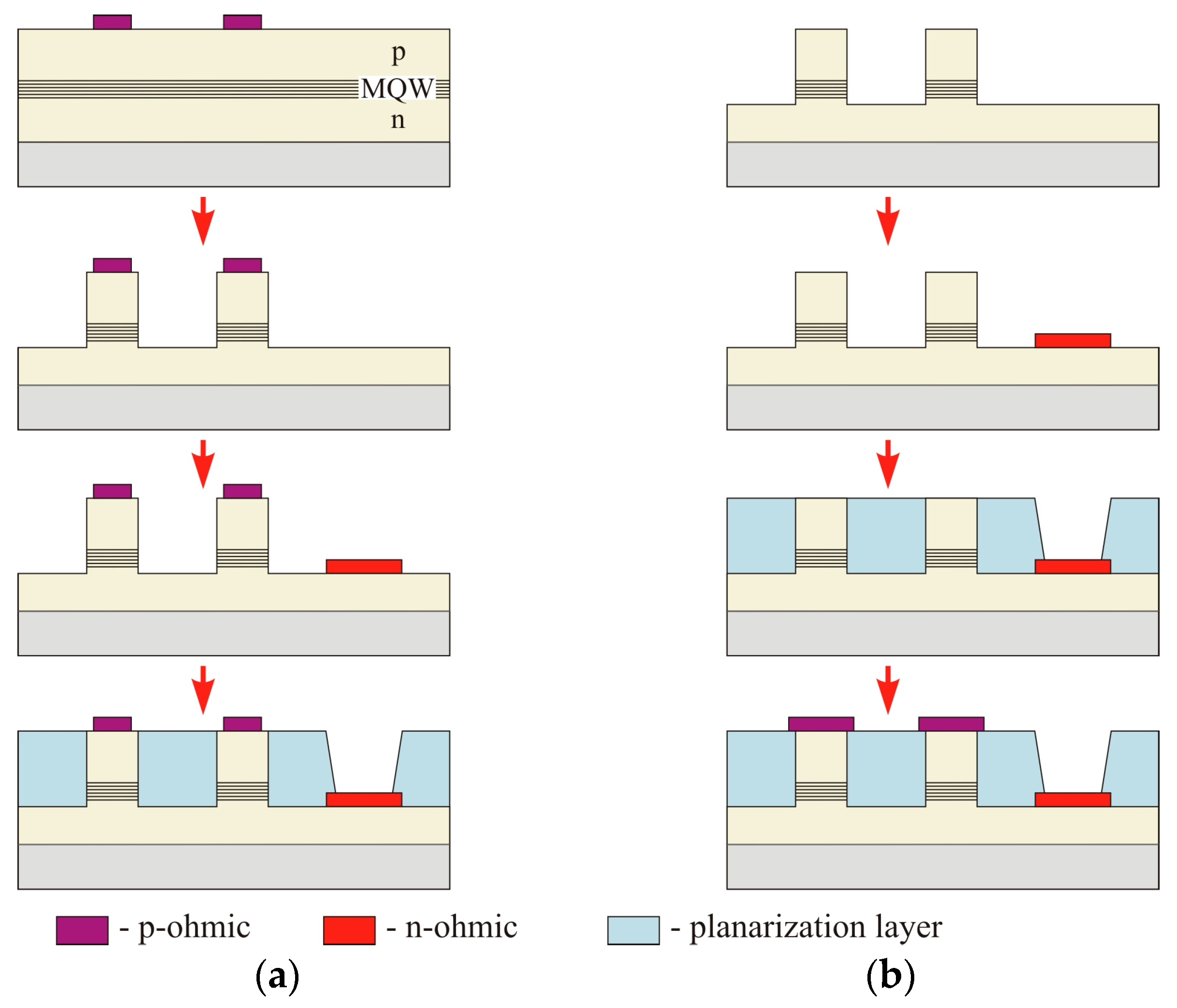
It is necessary to form p-i-n diodes to handle the phase of the optical wave in the arms of the modulator. A thin film composition of Ti/Pt/Au (50/25/400 nm) was used as the top ohmic contact to the p-InGaAs layer; the bottom ohmic contact to n-InP was formed on the basis of Ni/Ge/Au (10/30/200 nm). When developing a manufacturing process, the question arises, in what order should the formation of the ohmic contacts be carried out?
Figure 1 shows two manufacturing processes for the formation of the p-i-n diodes. In the first case (
Figure 1a), the top narrow p-contacts are formed first. The main advantage of this approach is the placement of ohmic contacts before the formation of the relief of the optical waveguides, which simplifies the lithography of the p-contacts. The width of the top ohmic contacts in this case is limited by the width of the optical waveguides and the required misalignment tolerances (depending on the lithographic equipment used). An additional limitation on the width is introduced by the probability of etching the Ti layer in the Ti/Pt/Au ohmic contact during etching of the heterostructure in chlorine-based plasma. This can lead to an increase in resistance or peeling of the ohmic contact. Therefore, the ohmic contact must be made narrower than the SiN
x mask so that the dielectric completely covers the ohmic metallization. It should also be taken into account that the Ti/Pt/Au ohmic contact has a lower annealing temperature of 300–350 °C [
22,
23], versus 410 °C, which was determined as optimal for Ni/Ge/Au (10/30/200 nm) metallization. This can lead to an increase in the resistance of the top ohmic contacts and a decline in the parameters of the modulator.
Figure 1b shows the second manufacturing process for the formation of p-i-n diodes. The transfer of the formation of the top ohmic contacts to the end of the manufacturing process simplifies the formation of optical waveguides because the restrictions discussed above do not apply here. In addition, the formation of the first bottom contact solves the problem of incompatibility of the annealing temperatures of the ohmic contacts. However, due to the high relief, it becomes difficult to perform lithography for the formation of narrow top ohmic contacts. First, the surface must be planarized, for which films of polyimide, BCB, polybenzoxazole (PBO), etc., can be used. An additional condition is that the planarizing film must withstand the annealing temperature of the Ti/Pt/Au ohmic contact without deformations. After hard baking, the glass transition temperature for BCB exceeds 350 °C [
24]. Furthermore, if it is possible to use the annealing temperature of the ohmic contact below 350 °C, BCB can be a candidate for surface planarization. Here it is also necessary to add a tolerance for the misalignment of the top ohmic contact with the optical waveguide. However, the tolerance can be set in the direction of increasing the width of the ohmic contact, which helps to reduce its resistance.
Another issue that needs to be addressed is the means of dividing a semiconductor wafer into single dies. In the manufacturing process of InP-based MZMs, the division of wafers is usually carried out by the cleaving method. Then, to reduce losses, an AR coating film is deposited on the die sides. The disadvantage of this approach is the need for deposition coating on single dies (or die blocks). Another method is to form the sides of the input/output waveguides directly on the wafer at the stage of etching the waveguides. This allows the AR coating to be deposited simultaneously on all chips of the wafer, before dividing it. In this case, lithographic methods remain available to restrict the areas of the AR- coating. Combinations of dicing, scribing, or deep wet etching methods, followed by the cleaving method, can be used to divide the wafer into single dies.
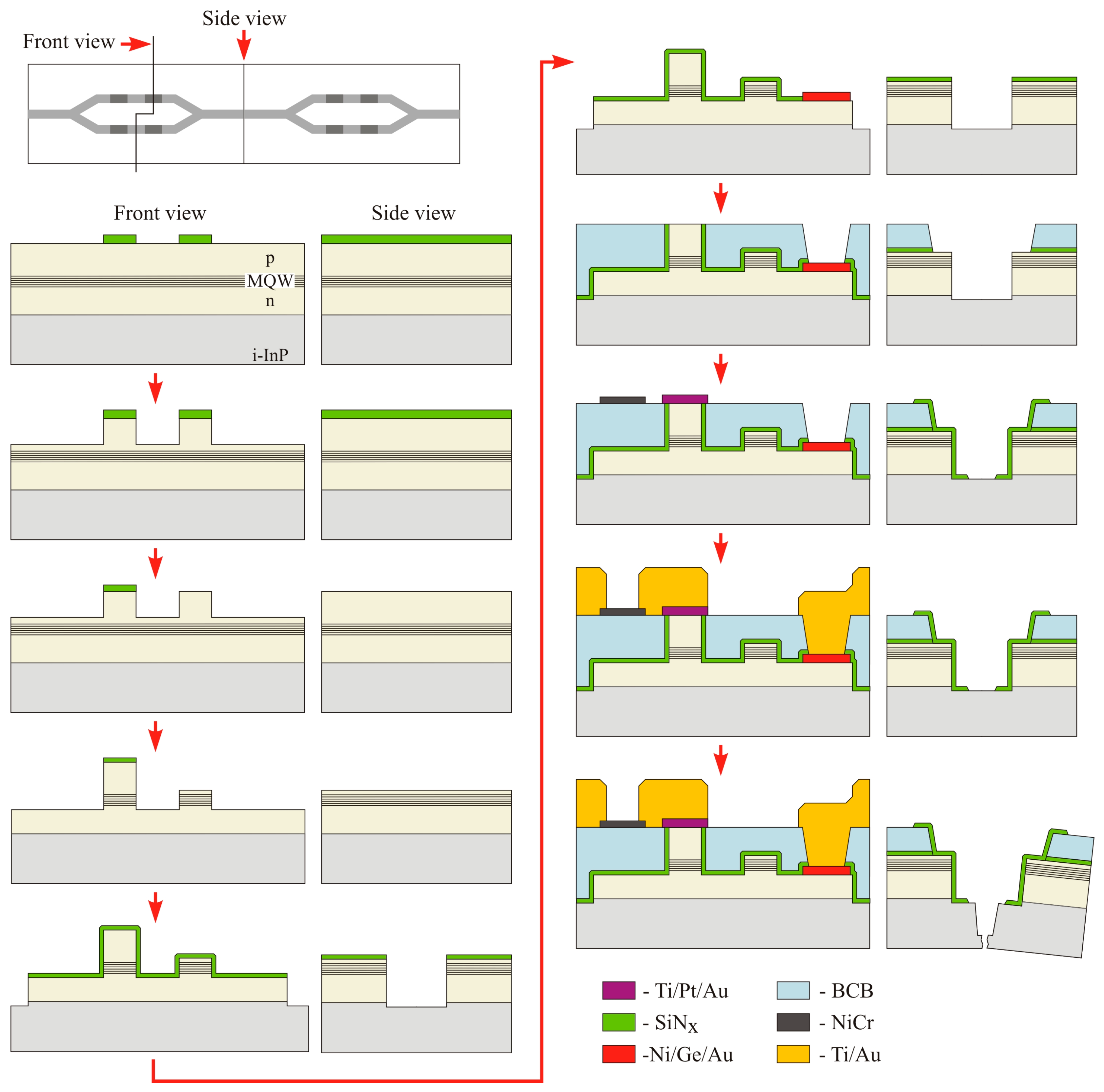
Taking into account the above stated theses, a manufacturing process was developed that consisted of the following sequence of technological blocks (
Figure 2):
formation of the SiNx dielectric mask for waveguide etching;
ICP etching of the p-layers of the heterostructure through the SiNx mask;
removing the SiNx dielectric mask from the passive elements of the electro-optical path;
ICP etching of the p- and i-layers of the heterostructure through the SiNx mask;
formation of the SiNx dielectric mask for the formation of mesa isolation;
ICP etching of the i- and n-layers of the heterostructure for the formation of mesa isolation and the edges of the waveguides at the optical input/outputs of the die;
formation of the Ni/Ge/Au ohmic contact to the n-InP layer of the heterostructure;
SiNx film deposition;
surface planarization with BCB film;
formation of the Ti/Pt/Au ohmic contact with the p-InGaAs layer of the heterostructure;
formation of the NiCr thin film resistors;
formation of the AR coating film (SiNx) on the sides of the modulator dies;
formation of the Ti/Au interconnect metallization;
formation of grooves along the boundaries of the dies (on a part of the wafer thickness);
final die division by cleaving.
3.2. MZM Fabrication
For optimization of the manufacturing process, test samples of the InP-based MZMs were fabricated. At the first stage, the optical waveguide elements of the modulator were fabricated using three sequential ICP etching processes through dielectric masks.
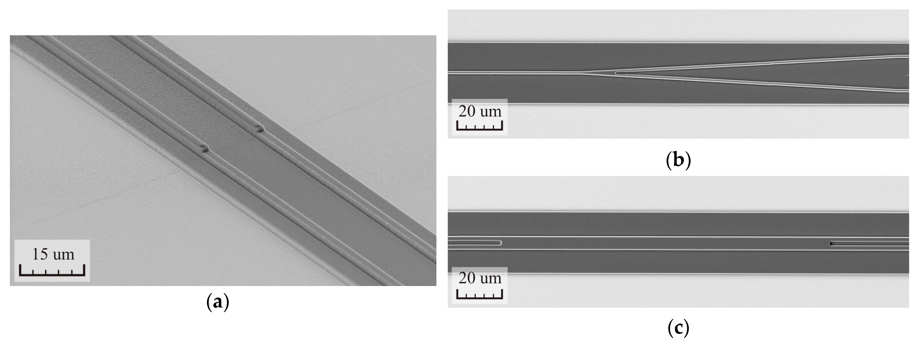
Figure 3 shows microscopic images of the waveguide elements of the modulator after the stage of forming the mesa isolation. The elements had an approximately rectangular profile and a smooth surface morphology. Formation of active and passive sections of the optical waveguides on the SiN
x mask prevents misalignment errors at the borders (
Figure 3a).
Furthermore, the bottom ohmic contacts of the p-i-n diodes were formed on the wafer. After annealing Ni/Ge/Au (10/30/200 nm) on a hotplate at a temperature of 410 °C for 2 min, the specific contact resistance of the ohmic contact was 1.2 × 10⁻⁶ Ohm∙cm2.
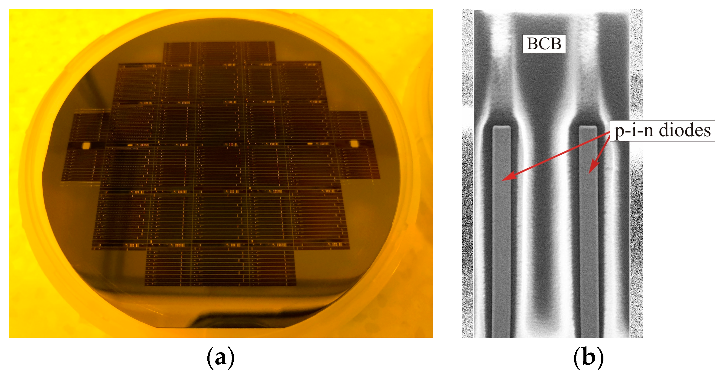
Figure 4 shows images of the wafer and fragment of the wafer surface in the region of the p-i-n diodes after planarization with the BCB film. After etching in SF
6/O
2 plasma, the BCB film had a smooth surface morphology. The difference in thickness of the film over the 3-inch wafer did not exceed 0.2 um.
Figure 4b shows the opened areas of the p-i-n diodes, whereas the remainder of the die surface was under the BCB film. This shows a good level of surface planarization.
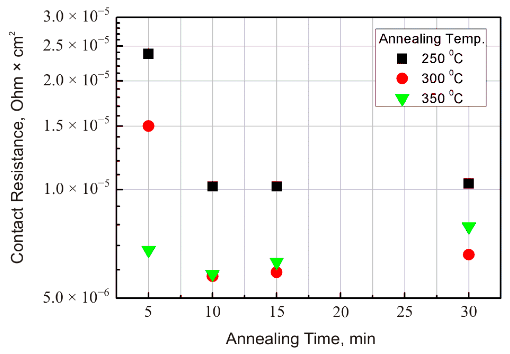
On the test wafer, the optimal temperature and time for annealing of the Ti/Pt/Au (50/25/400 nm) ohmic contact to p-InGaAs were determined before the formation of the top ohmic contacts of the p-i-n diodes. The annealing results are shown in
Figure 5. The optimal mode of annealing was heating the metallization to 300 °C for 10 min, and the minimum value of the specific contact resistance of 5.7 × 10
−6 Ohm∙cm
2 was achieved. An increase in the annealing temperature to 350 °C reduces the time required for annealing the ohmic contact. However, this does not lead to a decrease in its contact resistance. A decrease to 250 °C leads to an increase in the contact resistance. The obtained annealing temperature (300 °C) is significantly lower than the glass transition temperature of the BCB dielectric. Subsequent annealing of the ohmic contacts on the planarized wafers with the BCB film showed the absence of both deformation and cracking of the planarizing film.
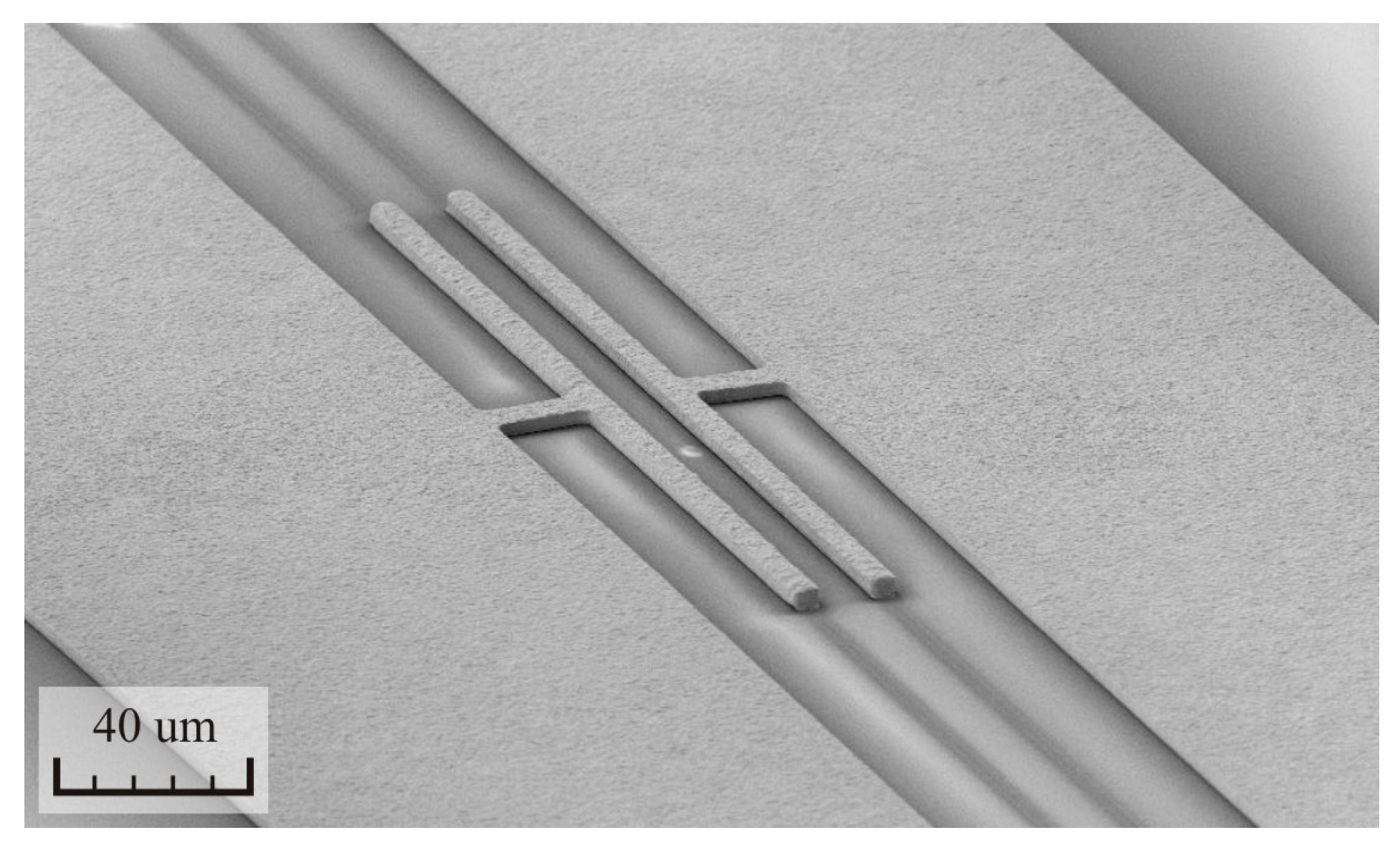
Figure 6 shows an SEM image of a fragment of the traveling wave electrode based on Ti/Au metallization with a thickness of 3 um. The figure shows the outer electrodes as a section of the inner electrodes electrically connected to the p-contacts of the p-i-n diodes of the phase-shifting section of the MZM. The BCB layer provides a sufficient level of planarization of the wafer surface.
Furthermore, the division of the wafers into single dies was performed using two techniques.
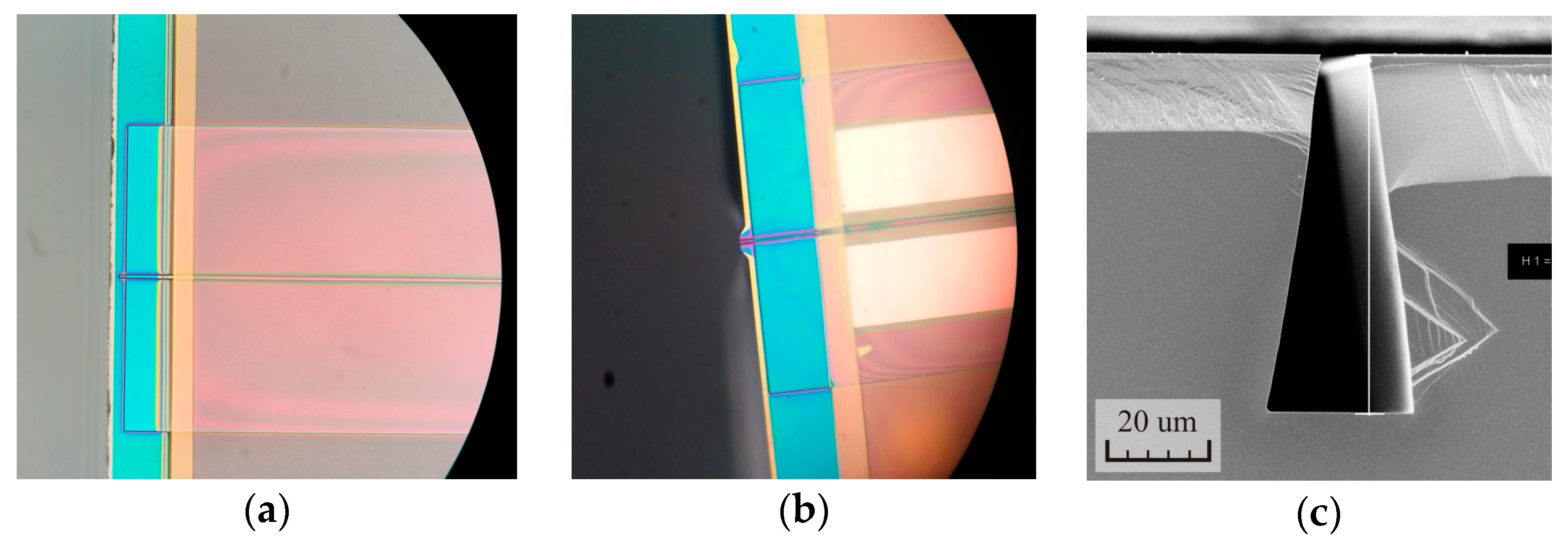
Figure 7a shows the edge of the die after dividing by assisted dicing. The dicing depth was 250 μm and the final die division was performed by cleaving. As can be seen from the figure, roughness is observed at the edge of the die, but its maximum depth inside the die area did not exceed 3 μm, whereas the prevailing roughness was 1–2 μm. In the second version, the groove was created using deep wet etching of InP in the HCl–water solution (1:3) through a single-layer photoresist mask (
Figure 7b,c); the final die division was also performed by cleaving. Here, the edge of the die was smooth without clear roughness. As can be seen from
Figure 7c, the etching process accounts for the crystallographic structure of the substrate material. The etching profile is trapezoidal with a wide bottom base. In this case, no further etching of the side faces was observed during the etching process. This allows the die edge to be placed as close to the edges of the input/output waveguides as the lithographic equipment allows. Both of the considered division techniques make it possible to obtain the minimum gap between the die and waveguide edges in a few microns. This is enough for subsequent coupling with optical fiber. In addition, the second technique allows more precise control of the gap.
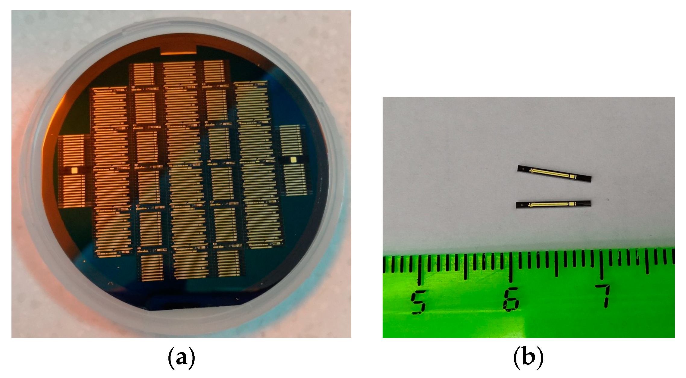
Figure 8 shows a photo of a semiconductor wafer with manufactured modulators and a photo of single dies of the modulators after division of the wafer. In this case, the division was performed with assisted dicing of a part of the wafer depth.
After measurements of these MZM prototypes, the following parameters were obtained (wavelength 1550 nm): a half-wave voltage of 2.9–3 V and an extinction ratio of 10–12 dB; the propagation loss in the test waveguides was 4.2 dB/cm. The achieved parameter values can be improved. At the next stage of this work, the authors will optimize both the heterostructure and the design of the topology of the MZM to achieve parameter values comparable to existing analogs. For this, in parallel with the development of the technology, a method was developed to optimize an InP-based electro-optical modulator [
25]. Thus, the results obtained confirm the possibility of manufacturing InP-based MZMs using the developed technology.
4. Conclusions
The paper presents the development of a technology for manufacturing InP-based Mach–Zehnder electro-optical modulators. The possibility of applying the ohmic Ti/Pt/Au (50/25/400 nm) to the p-InGaAs layer after wafer surface planarization with BCB film is shown. After annealing the ohmic contact, there was no deformation or cracking of the BCB film. New techniques for the division of the wafers into single dies are presented. The division was carried out in two stages: first, grooves were formed by dicing or deep wet etching, and then cleaving was performed along the formed grooves. The advantages of these techniques are that it allows the edges of the waveguides at the optical input/outputs to be formed and the antireflection coating to be deposited simultaneously on all dies on the wafer, before it is divided.
Author Contributions
Conceptualization, V.A. and P.T.; funding acquisition, V.A. and P.T.; investigation, S.I., V.A., I.Y., M.S. and Y.Z.; project administration, P.T.; resources, S.I. and V.A.; supervision, V.A.; validation, S.I., V.A., I.Y. and M.S.; writing—original draft, S.I.; writing—review and editing, S.I. All authors have read and agreed to the published version of the manuscript.
Funding
The work was carried out with financial support from the Ministry of Science and Higher Education of the Russian Federation (Project name: Theoretical and experimental studies of ultra-wideband optoelectronic devices of fiber-optic information systems and microwave photonics based on photonic integrated circuits own development, Agreement No. 075-03-2020-237/1 from 05.03.2020, project number: FEWM-2020-0040). Experimental results were obtained by the team of the Integrated Optics and Microwave Photonics Laboratory of the Tomsk State University of Control Systems and Radioelectronics using equipment of the “Impulse” center of collective usage (registration number 200568).
Conflicts of Interest
The authors declare no conflict of interest.
References
- Cisco Annual Internet Report. Available online: https://www.cisco.com/c/en/us/solutions/collateral/executive-perspectives/annual-internet-report/white-paper-c11-741490.html (accessed on 30 September 2020).
- NOKIA Who Will Satisfy the Desire to Consume? Available online: https://readymag.com/BellLabs/480968/ (accessed on 30 September 2020).
- Pleumeekers, J.L.; Schneider, R.P., Jr.; Mathur, A.; Hurtt, S.K.; Evans, P.W.; Dentai, A.G.; Joyner, C.H.; Lambert, D.J.H.; Murthy, S.; Muthiah, R.; et al. Status and progress in InP optoelectronic processing: Toward higher levels of integration. In Proceedings of the CS Mantech Conference, Vancouver, BC, Canada, 24–27 April 2006; pp. 115–118. [Google Scholar]
- Smit, M.; Leijtens, X.; Ambrosius, H.; Bente, E.; van der Tol, J.; Smalbrugge, B.; de Vries, T.; Geluk, E.J.; Bolk, J.; van Veldhoven, R.; et al. An introduction to InP-based generic integration technology. Semicond. Sci. Technol. 2014, 29, 083001. [Google Scholar] [CrossRef]
- Smit, M.; Williams, K.; van der Tol, J. Past, persent, and future of InP-based photonic integration. APL Photon. 2019, 4, 050901. [Google Scholar] [CrossRef] [Green Version]
- Soares, F.M.; Baier, M.; Gaertner, T.; Grote, N.; Moehrle, M.; Beckerwerth, T.; Runge, P.; Schell, M. InP-based foundry PICs for optical interconnections. Appl. Sci. 2019, 9, 1588. [Google Scholar] [CrossRef] [Green Version]
- Barton, J.S.; Skogen, E.J.; Masanovic, M.L.; Denbaars, S.P.; Coldren, L.A. A widely-tunnable high-speed transmitter using an integrated SGDBR laser-semiconductor optical amplifier and Mach-Zehnder modulator. IEEE J. Sel. Top. Quantum Electron. 2003, 9, 1113–1117. [Google Scholar] [CrossRef]
- Zhao, H.; Pinna, S.; Song, B.; Megalini, L.; Brunelli, S.T.S.; Coldren, L.A. Indium phosphide photonic integrated circuits for free space optical links. IEEE J. Sel. Top. Quantum Electron. 2018, 24, 1–6. [Google Scholar] [CrossRef] [PubMed]
- Ozaki, J.; Ogiso, Y.; Nakano, S. High-speed modulator for next-generation large-capacity coherent optical networks. Ntt Tech. Rev. 2018, 16, 1–8. [Google Scholar]
- Qian, G.; Niu, B.; Zhao, W.; Kan, Q.; Gu, X.; Zhou, F.; Kong, Y.; Chen, T. CL-TWE Mach-Zehnder electro-optic modulator based on InP-MQW optical waveguides. Chin. Opt. Lett. 2019, 17, 061301. [Google Scholar] [CrossRef]
- Schares, L.; Budd, R.; Kuchta, D.; Doany, F.E. Etched-facet semiconductor optical amplifiers for gain-integrated photonic switch fabrics. In Proceedings of the 2015 European Conference on Optical Communication, Valencia, Spain, 27 September–1 October 2015. [Google Scholar] [CrossRef]
- Research Topics of Modulator Group. Available online: https://www.hhi.fraunhofer.de/en/departments/pc/research-groups/modulators/research-topics.html (accessed on 30 September 2020).
- Letal, G.; Prosyk, K.; Millett, R.; Macquistan, D.; Paquet, S.; Thibault-Maheu, O.; Gagné, J.F.; Fortin, P.L.; Dowlatshahi, R.; Rioux, B.; et al. Low Loss InP C-Band IQ Modulator with 40 GHz Bandwidth and 1.5 V Vp. In Proceedings of the Optical Fiber Communication Conference, Los Angeles, CA, USA, 22–26 March 2015. [Google Scholar] [CrossRef]
- DWDM and Coherent Optical Transceivers. Available online: https://www.lumentum.com/en/optical-communications/products/dwdm-and-coherent-optical-transceivers (accessed on 30 September 2020).
- Yamanaka, T.; Tsuzuki, K.; Kikuchi, N.; Fukano, H. High-performance InP-based Optical Modulators. Ntt Tech. Rev. 2006, 4, 39–44. [Google Scholar]
- Yagi, H.; Yoneda, Y.; Ekawa, M.; Shoji, H. InP-Based Monolithic Integration Technologies for 100/200 Gb/s Pluggable Coherent Transceivers. IEICE Trans. Electron. 2017, E100.C, 179–186. [Google Scholar] [CrossRef] [Green Version]
- Sekiguchi, S.; Akiyama, S.; Itoh, H.; Yamamoto, T. InP-Based Mach–Zehnder Modulator with Capacitively Loaded Traveling-Wave Electrodes. J. Lightwave Technol. 2008, 26, 608–615. [Google Scholar] [CrossRef]
- Poirier, M.; Boudreau, M.; Lin, Y.-M.; Narayan, R.; Chen, C.; Hong, X.; Olson, R.; Liu, X.; Gokhale, M.; Ma, Y.; et al. InP Integrated Coherent Transmitter for 100 Gb/s DP-QPSK transmission. In Proceedings of the Optical Fiber Communication Conference, Los Angeles, CA, USA, 22–26 March 2015. [Google Scholar] [CrossRef]
- Deng, L. Dry etching of InP-based materials using a high-density ICP plasma system. Semicond. Today Compd. Adv. Silicon 2012, 7, 82–87. [Google Scholar]
- Carlstrom, C.F.; Andriesse, M.S.P.; Karouta, F.; Heijden, R. Comparative study of Cl2, Cl2/O2, and Cl2/N2 inductively coupled plasma processes for etching of high-aspect-ratio photonic crystals holes in InP. J. Vac. Sci. Technol. B 2008, 26, 1675–1683. [Google Scholar] [CrossRef]
- Siwak, N.P.; Fan, X.Z.; Ghodssi, R. Fabrication challenges for indium phosphide Microsystems. J. Micromech. Microeng. 2015, 25, 1317–1331. [Google Scholar] [CrossRef]
- Integration of Multiwavelength Lasers with Fast Electro-Optical Modulators. Available online: https://pure.tue.nl/ws/files/2032094/200413118.pdf (accessed on 30 September 2020).
- Ively, D.G.; Ingrey, S.; Noel, J.-P.; Lau, W.M. Micro structural study of Ti/Pt/Au contacts to p-InGaAs. J. Mater. Sci. Eng. B 1997, 49, 66–73. [Google Scholar] [CrossRef]
- Advanced Packaging Polymers. Available online: https://www.microresist.de/en/?jet_download=4823 (accessed on 30 September 2020).
- Stepanenko, M.; Yunusov, I.; Arykov, V.; Troyan, P.; Zhidik, Y. Multi-Parameter Optimization of an InP Electro-Optic Modulator. Symmetry 2020, 12, 1920. [Google Scholar] [CrossRef]
| Publisher’s Note: MDPI stays neutral with regard to jurisdictional claims in published maps and institutional affiliations. |
© 2020 by the authors. Licensee MDPI, Basel, Switzerland. This article is an open access article distributed under the terms and conditions of the Creative Commons Attribution (CC BY) license (http://creativecommons.org/licenses/by/4.0/).
