Abstract
In a triple-well NMOSFET, a deep n+ well (DNW) is buried in the substrate to isolate the substrate noise. The presence of this deep n+ well leads to changes in single-event transient effects compared to bulk NMOSFET. In space, a single cosmic particle can deposit enough charge in the sensitive volume of a semiconductor device to cause a potential change in the transient state, that is, a single-event transient (SET). In this study, a quantitative characterization of the effect of a DNW on a SET in a 65 nm triple-well NMOSFET was performed using heavy ion experiments. Compared with a bulk NMOSFET, the experimental data show that the percentages of average increase of a SET pulse width are 22% (at linear energy transfer (LET) = 37.4 MeV·cm2/mg) and 23% (at LET = 22.2 MeV·cm2/mg) in a triple-well NMOSFET. This study indicates that a triple-well NMOSFET is more sensitive to a SET, which means that it may not be appropriate for radiation hardened integrated circuit design compared with a bulk NMOSFET.
1. Introduction
Along with the wide application of electronic technology in the aerospace field, research on single-event effects of integrated circuits (ICs) has become ever more important. With technology scaling to deep submicron dimensions, single-event transients (SETs) have gradually become a key source of logical errors in ICs, becoming one of the main concerns for researchers [1,2,3,4,5,6]. The physical mechanisms of charge motion of SETs have been verified; the diffusion charge collection effect of sensitive nodes and charge collection effect of parasitic bipolar transistors are two main mechanisms of SETs in a bulk CMOS technology [4]. Nevertheless, the characterization of experimental data on SETs is still rarely reported up to now. In virtue of the inherent non-instantaneity and nature of a SET pulse, SET mitigation has always been a challenging task in the field of reliability [1].
The physical mechanisms of charge motion on SETs have been extensively studied in bulk NMOSFETs and triple-well NMOSFETs [4,5,6,7,8,9]. These issues have also been extensively studied in our previous works [10,11,12,13,14]. The process of charge motion on SETs is controlled by drift, diffusion, and amplification effect of a parasitic bipolar transistor. In a bulk NMOSFET, the charge motion is primarily controlled by diffusion and drift, and the other control effects are not obvious. However, in a triple-well NMOSFET, the amplification effect of a parasitic bipolar transistor becomes the main factor due to the deep n+ well (DNW) changing the rate of diffusion of electrons and holes, leading to higher probability of SET. In these works [8,9], all of the results just come from device simulations. The effects of space particles on microcircuits in aerospace have been studied for many years. Because of the effects of space particles, a large number of charges accumulate at the sensitive nodes of semiconductor devices to bring about single-event transients (SETs); more studies need to be conducted in heavy ion experiments for quantitative verification.
Triple-well technologies are extensively used in analog and mixed ICs because of their excellent noise immunity as a result of the isolation of the DNW from the substrate [15]. Because it is easy to modulate threshold voltage by using well bias, triple-well technologies are also extensively used in storage circuits. However, when these circuits are used in aerospace electronic instruments, they are exposed to the radiation of particles making the effects of particles on these circuits an important research issue. In our previous works, the characterization of single-event multiple cell transients in a custom SRAM was studied in a 65 nm triple-well CMOS technology. It was found that this SRAM is very sensitive to single-event multiple cell upsets (MCUs) compared with that in the bulk CMOS technology [16]. The pulse quenching on SETs in this SRAM also became more significant than that in the bulk CMOS technology [14]. However, the quantitative characterization of the effect of DNW on SET in 65 nm triple-well NMOSFETs is still not demonstrated in heavy ion experiments. In order to quantify the effect of DNW on SET in 65 nm triple-well NMOSFETs, the test chips were manufactured by 65 nm domestic bulk CMOS process technology and triple-well CMOS technology. The N-hit cell and chain, proposed by Gadlage for NMOSFET SET production and propagation [6], were introduced in our work.
2. Device and Simulation Details
In this study, an inverter was used to simulate the SET production process. The NMOSFET was modeled with a three dimensional digital model and the PMOSFET was modeled with a SPICE model. Both the simulation of the bulk NMOSFET and the triple-well NMOSFET were investigated. The n-well contact (nc) and drain (d) were connected to high voltage level (“1”) and the source (s), gate (g) and p-substrate contact (pc) were connected to GND (“0”) in the simulation. In this study, angular effects were not discussed. Heavy ion strikes were taken as perpendicular to the center of the drain (d) of the NMOSFET.
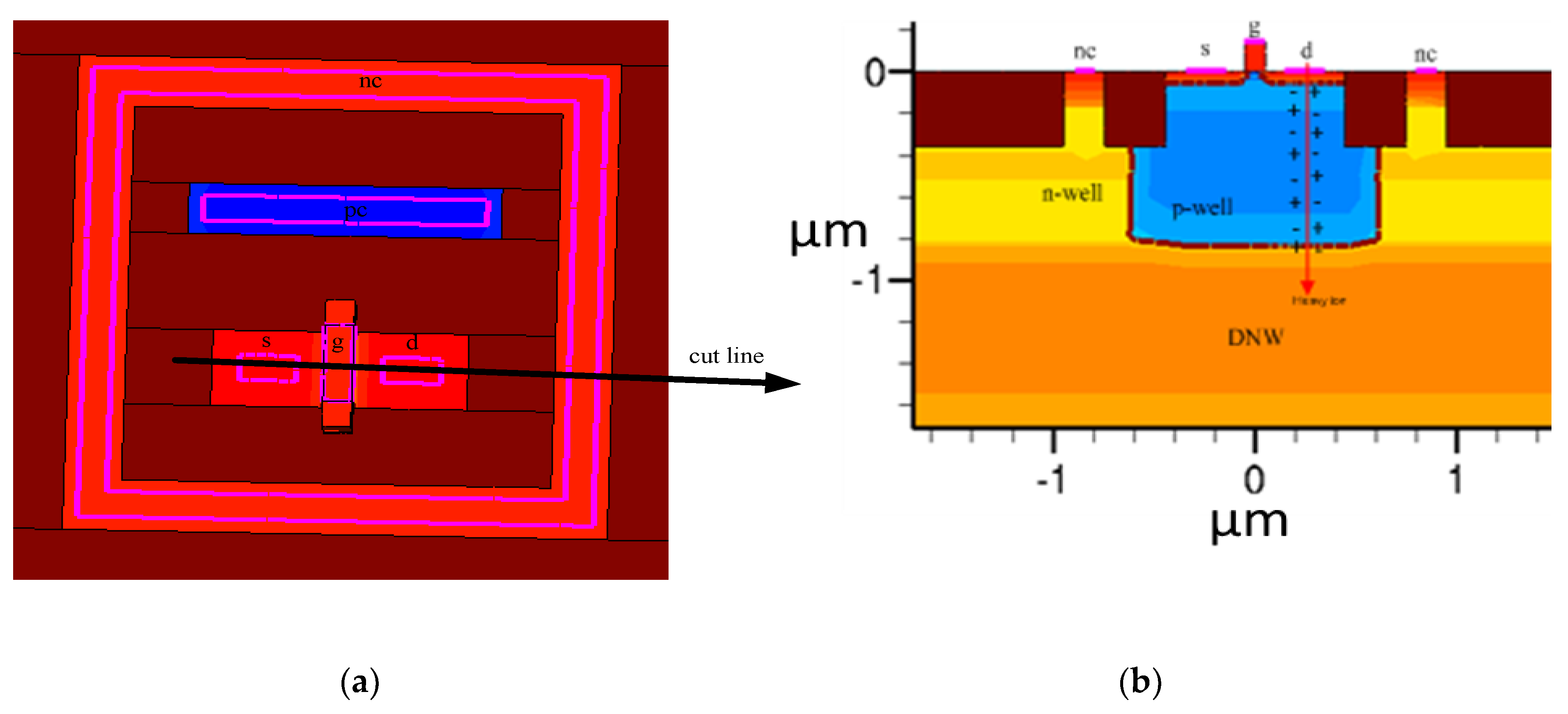
Sentaurus TCAD from Synopsys was used in the research to design the device and execute the simulations. The domestic 65nm bulk NMOSFET and triple-well NMOSFET were studied. According to the design rule from the foundry, the DNW was buried in the substrate and under the p-well which was surrounded by the n-well. Figure 1a represents the top view of the triple-well NMOSFET, and Figure 1b represents the cross-section view of the triple-well NMOSFET. Correspondingly, the structure of the bulk NMOSFET was similar, without the DNW and the n-well. The 65 nm bulk NMOSFET and triple-well NMOSFET were built and calibrated according to the SMIC 65 PDK. The W/L ratio of the bulk NMOSFET was 0.3/0.06 μm in the TCAD model and the W/L ratio of the PMOSFET was 0.6/0.06 μm in the SPICE model.
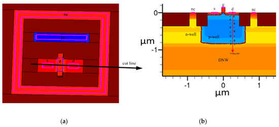
Figure 1.
Triple-well NMOSFET: (a) top view and (b) cross-section view.
Heavy ion striking was modeled with a cylinder of electron–hole pairs along the heavy ion trajectory. The linear energy transfer value remained constant. The length of ion trajectory was 10 μm and the radius of the ion trajectory was 0.1 μm. The two types of NMOSFETs for the simulation were identical to those in our previous work [10,11,12,13,14].
3. Simulation Results and Discussion
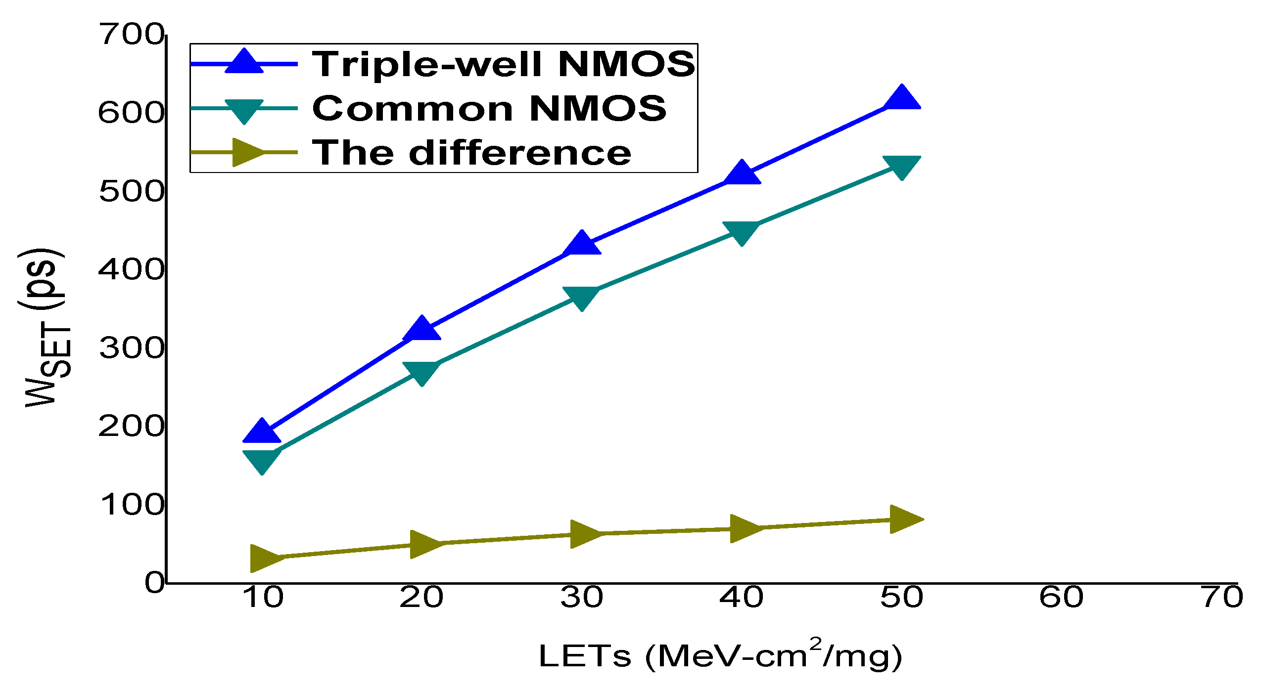
The SET pulse widths (WSET) produced in the bulk NMOSFET and triple-well NMOSFET are shown in Figure 2. The pulse width is defined as the width between 50% of the rising and falling edges of the pulse amplitude. As shown in Figure 2, the WSET in the bulk NMOSFETs was smaller than that in triple-well NMOSFETs. The difference is also shown in Figure 2. When the linear energy transfer (LET) is 10 MeV∙cm2/mg, the difference is 32 ps. When the linear energy transfer (LET) is 50 MeV∙cm2/mg, the difference is more significant, reaching 82 ps.
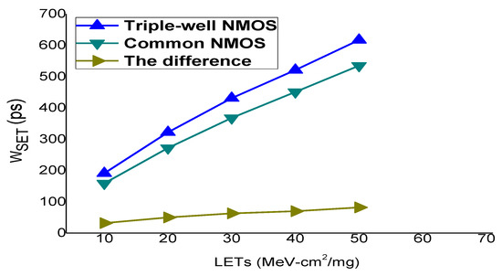
Figure 2.
Values of SET pulse widths (WSET) in bulk NMOSFET and triple-well NMOSFET.
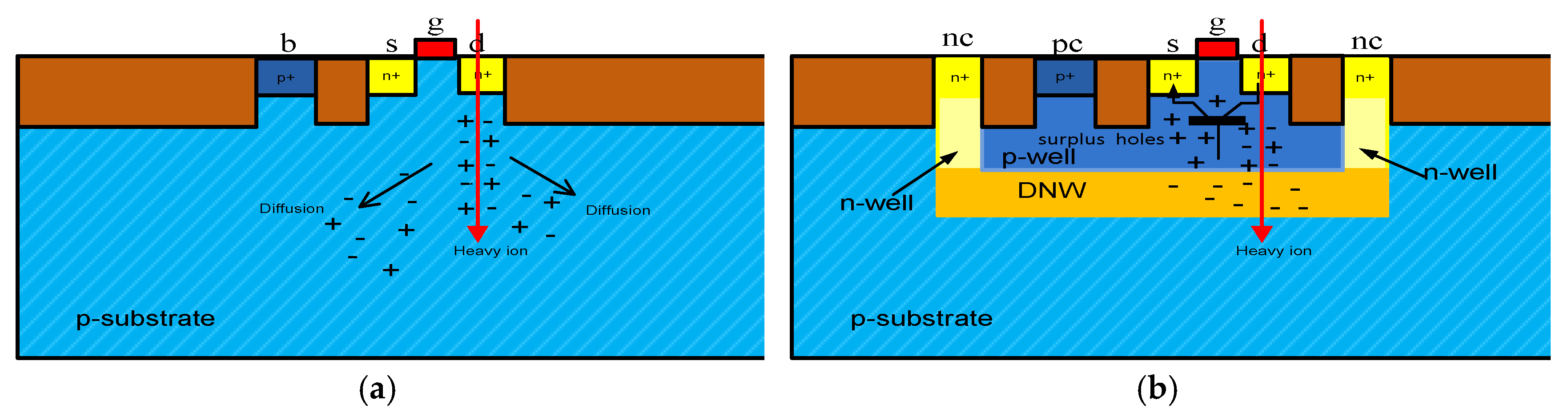
After a heavy ion strike at the center of the drain of the bulk NMOSFET in a normal strike, numerous generated electron-hole pairs were generated along the ion trajectory, as shown in Figure 3a. The drain collected the generated electrons, making a SET appear at the output of the inverter. Electron–hole pairs generated by the strike were dispersed in the substrate at the same probability, so the bulk potential was not increased significantly. The parasitic bipolar transistor (BJT) consisting of source–bulk–drain is not activated and the bipolar effect is insignificant in the bulk NMOSFET.
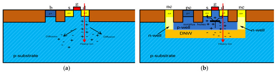
Figure 3.
Cross-sections of the two types of NMOSFET: (a) bulk NMOSFET and (b) triple-well NMOSFET.
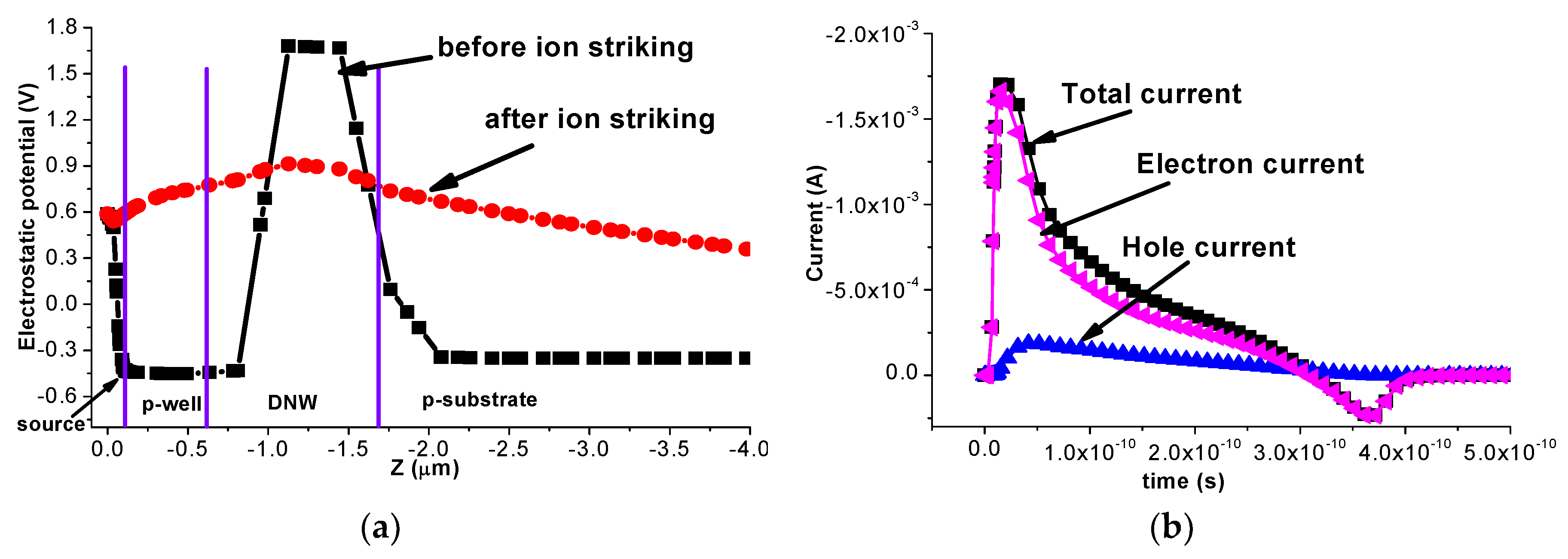
After a heavy ion strike at the center of the drain of the bulk NMOSFET in a normal strike, as shown in Figure 3b, the generated holes were prevented from entering the substrate by PN junctions, which were located between the p-well and the DNW. The excess holes led to an increased p-well potential (as shown in Figure 4a). The parasitic BJT is activated: A large number of electrons were injected into the p-well and drifted to the drain eventually (as shown in Figure 4b). The electrons collected by the drain will increase, causing an increase in WSET.

Figure 4.
Potential distribution along Z-axis and the current components of the source of the triple-well NMOSFET. (a) Potential distribution along Z-axis cutline before ion striking and after 50 ps of ion striking; (b) Source current components.
4. Quantitative Characterization
As shown in Figure 5, the N-hit cell and chain, proposed by Gadlage for NMOSFET SET production and propagation [6], are introduced in our work. In this chain, an off-state PMOSFET in inverter cell or an off-state NMOSFET in the NAND cell can produce “010” SET or “101” SET. However, the “010” SET produced in a PMOSFET cannot propagate through the chain due to the logic shield of the NAND cell. Therefore, only the “101” SET produced in a NMOSFET can travel through the chain and be captured by the terminal SET monitoring circuit, which was proposed by Narasimham [17]. In our circuit, four short 200-stage N-hit chains are in turn connected to an OR logic cell, which is connected to the SET monitoring circuit.
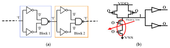
Figure 5.
(a) N-hit chain and (b) N-hit cell.
A Field Programmable Gate Array (FPGA) undertook monitoring the heavy ion experimental results. In order to avoid the computer being affected by radiation, the computer was located outside the heavy ion radiation room and connected to the FPGA. SETs captured were recorded by FPGA, and saved on the computer for subsequent analysis. The test chips were irradiated using two heavy ions: Ti (LET = 22.2 MeV·cm2/mg) and Ge (LET = 37.4 MeV·cm2/mg) were used. The experiments were carried out at the HI-13 Tandem Accelerator in the China Institute of Atomic Energy, Beijing. The SETs during 1 × 10⁷ ions/cm2 strikes were recorded.
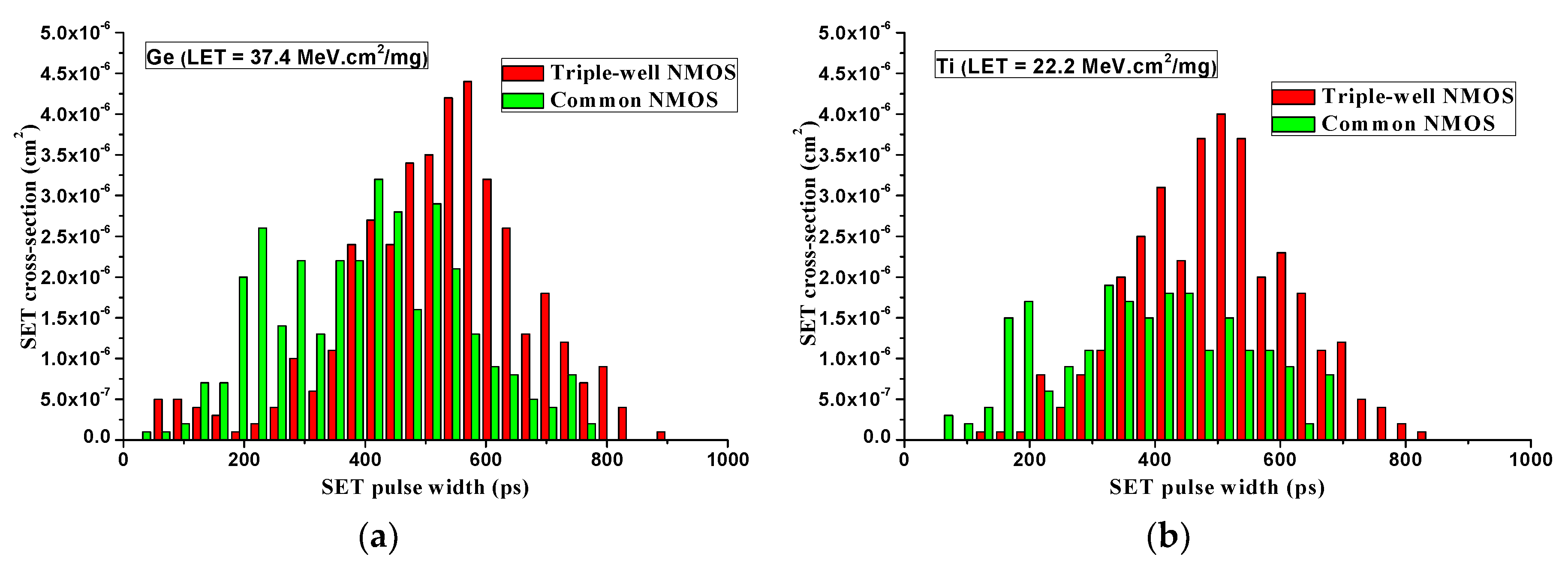
The cross-sections of captured single-event transients in the bulk NMOSFET and triple-well NMOSFET are shown in Figure 6 and Figure 7 at Ge (LET = 37.4 MeV·cm2/mg) and Ti (LET = 22.2 MeV·cm2/mg) exposures. Compared with the bulk NMOSFET, Figure 6a indicates that the total single-event transients cross-section at Ge (LET = 37.4 MeV·cm2/mg) exposure increased significantly in the triple-well NMOSFET. At the larger areas, the number of monitored SETs is found to significantly decrease in the bulk NMOSFET. The comparison of SET areas in these two types of NMOSFETs under Ti irradiation is shown in Figure 6b. The distribution in Figure 6a,b is similar. Not only is the number of monitored SETs found to significantly decrease in the bulk NMOSFET, but also WSET is significantly decrease.
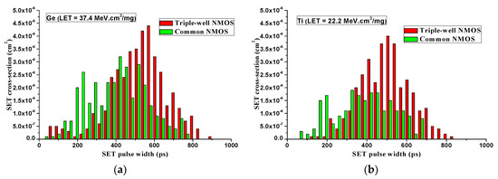
Figure 6.
Comparison of single-event transient (SET) pulse widths in bulk NMOSFET and triple-well NMOSFET (a) at Ge irradiation and (b) at Ti irradiation.
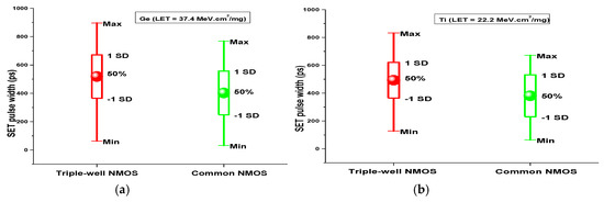
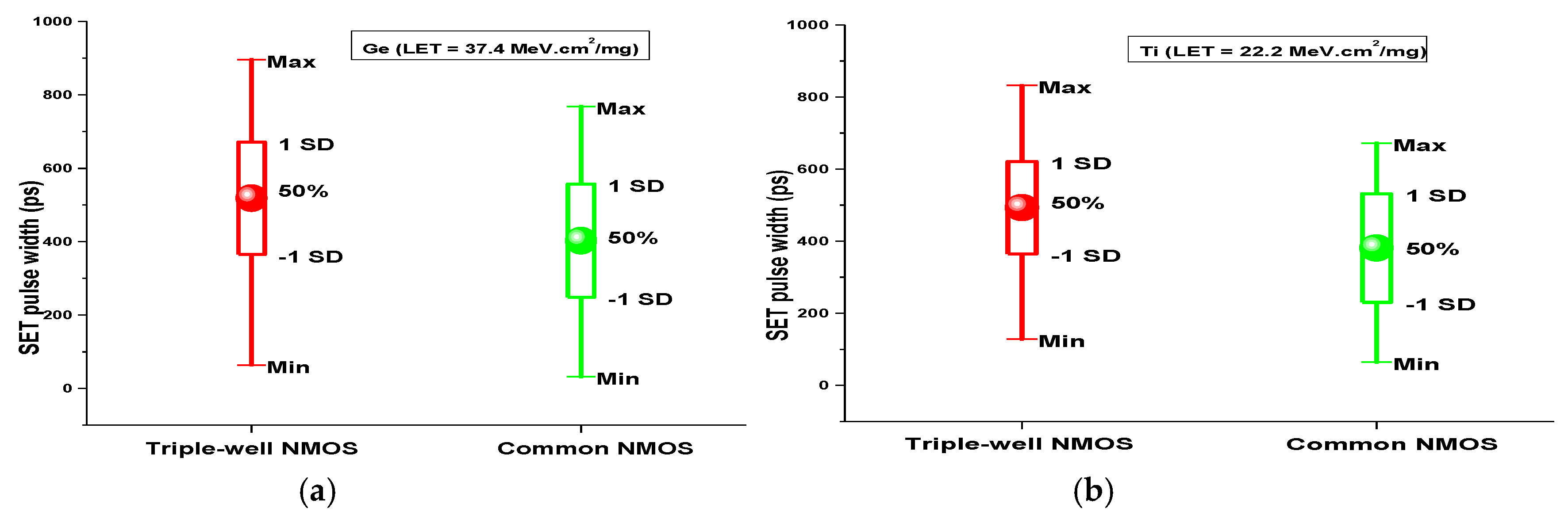
Figure 7.
Maximum, average, minimum and ±1 standard deviation SET pulse widths in bulk NMOSFET and triple-well NMOSFET (a) at Ge irradiation and (b) at Ti irradiation.
Figure 7 indicates the maximum, average, minimum and ±1 standard deviation of WSET in the two types of NMOSFET. At Ge (LET = 37.4 MeV·cm2/mg) irradiation, the average WSET of 403 ps was observed in the bulk NMOSFET, while the average WSET of 518 ps appeared in the triple-well NMOSFET showing an increase of 115 ps. At Ti (LET = 22.2 MeV·cm2/mg) irradiation, the average WSET was 493 ps in the triple-well NMOSFET, while it was 381 ps in the bulk NMOSFET, exhibiting a reduction of 112 ps. The experimental results of radiation show the percentages of average reduction of WSET were 22% (Ge_LET = 37.4 MeV·cm2/mg) and 23% (Ti_LET = 22.2 MeV·cm2/mg) in the bulk NMOSFET compared with that in the triple-well NMOSFET [18].
The experimental results show that the triple-well NMOSFET is more sensitive to SET, which means that triple-well NMOSFETs may not be suitable for the design of integrated circuits for aerospace environments.
5. Conclusions
In this study, the simulation results and experimental characterization of the effect of DNW on SET in 65 nm triple-well NMOSFETs were investigated in heavy ion experiments. Compared with a bulk NMOSFET, the experimental data show that the percentages of average increase of SET pulse width were 22% (Ge_LET = 37.4 MeV·cm2/mg) and 23% (Ti_LET = 22.2 MeV·cm2/mg) in a triple-well NMOSFET. Research has proved that triple-well NMOSFET technology has the natural disadvantage in the design of radiation hardened integrated circuits and may not be used in the design of integrated circuits in radiation environments. Referring to other studies, the next step is to do further specific experiments on SOI and FIN structures for quantitative characterization.
Author Contributions
Conceptualization, J.Z., J.C.; methodology, J.Z., J.C.; validation, P.H., S.L.; simulation, J.Z.; formal analysis and investigation, J.Z.; writing original draft preparation, writing and editing, J.Z.; visualization and supervision, L.F.; funding acquisition, J.C.
Funding
This work was supported by the Institute of Microelectronics, College of Computer, National University of Defense Technology, Changsha 410073, China. This work was also partly supported by the Institute for Quantum Information & State Key Laboratory of High Performance Computing, College of Computer, National University of Defense Technology, Changsha 410073, China. This work is co-funded by the National Natural Science Foundation of China (Grant No. 61504169 and 61434007).
Conflicts of Interest
The authors declare no conflict of interest.
References
- Cavrois, V.F.; Massengill, L.W.; Gouker, P. Single event transients in digital CMOS A review. IEEE Trans. Nucl. Sci. 2013, 60, 1767–1790. [Google Scholar] [CrossRef]
- Huang, P.; Chen, S.; Chen, J.; Liu, B. Novel N-hit single event transient mitigation technique via open guard transistor in 65 nm bulk CMOS process. Sci. China Tech. Sci. 2013, 56, 271–279. [Google Scholar] [CrossRef]
- Chen, J.; Chen, S.; Liang, B.; Liu, F. Single event transient pulse attenuation effect in three-transistor inverter chain. Sci. China Tech. Sci. 2012, 55, 867–871. [Google Scholar] [CrossRef]
- Amusan, O.A.; Witulski, A.F.; Massengill, L.W.; Bhuva, B.L.; Fleming, P.R.; Alles, M.L.; Sternberg, A.L.; Black, J.D.; Schrimpf, R.D. Charge collection and charge sharing in a 130 nm C-MOS technology. IEEE Trans. Nucl. Sci. 2006, 53, 3253–3258. [Google Scholar] [CrossRef]
- Jagannathan, S.; Gadlage, M.J.; Bhuva, B.L.; Schrimpf, R.D.; Narasimham, B.; Chetia, J.; Ahlbin, J.R.; Massengill, L.W. Independent measurement of SET pulse widths from N-hits and P-hits in 65-nm CMOS. IEEE Trans. Nucl. Sci. 2010, 57, 3386–3391. [Google Scholar] [CrossRef]
- Gadlage, M.J.; Ahlbin, J.R.; Narasimham, B.; Bhuva, B.L.; Massengill, L.W.; Schrimpf, R.D. Single-event transient measurements in nMOS and pMOS transistors in a 65-nm bulk CM-OS technology at elevated temperatures. IEEE Trans. Device Mater. Rel. 2011, 1, 179–186. [Google Scholar] [CrossRef]
- Amusan, O.A.; Masengill, L.W.; Bhuva, B.L.; DasGupta, S.; Witulski, A.F.; Ahlbin, J.R. Design techniques to reduce SET pulse widths in deep-submicron combinational logic. IEEE Trans. Nucl. Sci. 2007, 54, 2060–2064. [Google Scholar] [CrossRef]
- Roy, T.; Witulski, A.F.; Schrimpf, R.D.; Alles, M.L.; Massengile, L.W. single Event Mechanisms in 90 nm Triple-Well CMOS Devices. IEEE Trans. Nucl. Sci. 2008, 55, 2948–2956. [Google Scholar] [CrossRef]
- He, Y.B.; Chen, S.M. Simulation study of the selectively implanted deep-N-well for PMOS SET mitigation. IEEE Trans. Device Mater. Rel. 2014, 14, 99–103. [Google Scholar]
- Chen, J.J.; Chen, S.M.; He, Y.B.; Chi, Y.Q.; Qin, J.R.; Liang, B.; Liu, B.W. Novel layout technique for N-hit single-event transient mitigation via source-extension. IEEE Trans. Nucl. Sci. 2012, 59, 2859–2866. [Google Scholar] [CrossRef]
- Chen, J.; Chen, S.; Liang, B.; Liu, B.; Liu, F. Radiation hardened by design techniques to reduce single event transient pulse width based on the physical mechanism. Microelectron. Reliab. 2012, 52, 1227–1232. [Google Scholar] [CrossRef]
- Chen, J.J.; Chen, S.M.; He, Y.B.; Qin, J.R.; Liang, B.; Liu, B.W.; Huang, P.C. Novel layout technique for single-event transient mitigation using dummy transistor. IEEE Trans. Device Mater. Rel. 2012, 13, 177–184. [Google Scholar] [CrossRef]
- Chen, J.J.; Chen, S.M.; Liang, B.; Liu, B.W. Simulation study of the layout technique for P-hit single-event transient mitigation via the source-isolation. IEEE Trans. Device Mater. Rel. 2012, 12, 501–509. [Google Scholar] [CrossRef]
- Chen, J.J.; Chen, S.M.; Chi, Y.Q.; Liang, B. Characterization of single-event transient pulse quenching among dummy gate isolated logic nodes in 65nm twin-well and triple-well CMOS technologies. IEEE Trans. Nucl. Sci. 2015, 62, 2302–2309. [Google Scholar]
- Bevilacqua, A.; Niknejad, A.M. An ultra-wideband CMOS low noise amplifier for 3.1–10.6-GHz wireless receivers. IEEE J. Solid-St Circ. 2004, 39, 2259–2268. [Google Scholar] [CrossRef]
- Chen, H.Y.; Chen, J.J.; Yao, L. Characterizations of the effect of vertical well isolation on single-event multiple cell upsets in SRAM in a 65nm triple-well CMOS technology. Sci. China Tech. Sci. 2015, 58, 1726–1730. [Google Scholar] [CrossRef]
- Narasimham, B.; Ramachandran, V.; Bhuva, B.L.; Schrimpf, R.D.; Witulski, A.F.; Holman, W.T.; Massengill, L.W.; Black, J.D.; Robinson, W.H.; McMorrow, D. On-chip Characterization of single-Event Transient Pulsewiths. IEEE Trans. Device Mater. Rel. 2006, 6, 542–549. [Google Scholar] [CrossRef]
- Xu, J.Y.; Chen, S.M.; Song, R.Q.; Wu, Z.Y.; Chen, J.J. Analysis of Single-Event Transient Sensitivity in Fully-Depleted Silicon-on-Insulator MOSFETs. Nucl. Sci. Tech. 2018, 29, 49–54. [Google Scholar] [CrossRef]

© 2019 by the authors. Licensee MDPI, Basel, Switzerland. This article is an open access article distributed under the terms and conditions of the Creative Commons Attribution (CC BY) license (http://creativecommons.org/licenses/by/4.0/).