Metal–Insulator Transition in Three-Dimensional Semiconductors


Institut für Physik, Universität Augsburg, D-86135 Augsburg, Germany
Symmetry 2019, 11(11), 1345; https://doi.org/10.3390/sym11111345
Submission received: 28 September 2019
/
Revised: 21 October 2019
/
Accepted: 24 October 2019
/
Published: 1 November 2019
(This article belongs to the Special Issue Symmetry and Mesoscopic Physics)
Abstract
:We use a random gap model to describe a metal–insulator transition in three-dimensional semiconductors due to doping, and find a conventional phase transition, where the effective scattering rate is the order parameter. Spontaneous symmetry breaking results in metallic behavior, whereas the insulating regime is characterized by the absence of spontaneous symmetry breaking. The transition is continuous for the average conductivity with critical exponent equal to 1. Away from the critical point, the exponent is roughly 0.6, which may explain experimental observations of a crossover of the exponent from 1 to 0.5 by going away from the critical point.
1. Introduction
The particle-hole symmetry plays a crucial role in solid state physics. In particular in semi- as well as in superconductor physics [1], this symmetry appears due to the existence of two separate bands. Recent theoretical studies of three-dimensional Weyl materials has renewed interest in the disordered driven metal–insulator transition [2,3,4,5,6,7,8,9,10,11,12,13,14,15,16,17,18,19,20,21,22,23,24,25,26]. It was shown recently that Anderson localization can be prevented even in the strong disorder regime when particle-hole symmetry is present [27,28]. This can be understood by the simple picture that particle-hole pairs can be created by an infinitesimal excitation energy.
Undoped semiconductors have a small gap between the valence and the conduction band, typically of the order of eV [1]. This gap is strongly affected by doping, which allows us to engineer a variety of useful technological applications. In particular, sufficiently strong doping closes the gap such that a metallic phase appears. A classical example for this type of metal–insulator transition is doped silicon, where typical dopants are phosphorus (Si:P) or boron (Si:B) [29,30,31,32,33]. Disorder plays a crucial role in these materials due to the inhomogeneous distribution of the dopants. This suggested that Anderson localization must play a crucial role in these systems, where the quantum states would undergo a transition from extended to localized states for increasing disorder. This transition should be reflected in the transport properties, where extended states lead to a metal and localized states to an insulator at vanishing temperatures.
Measurements of the conductivity as a function of doping concentration N in Si:P at low temperatures has indeed revealed a critical behavior. Above a critical concentration a power law was found
and a vanishing conductivity for . The exponent was determined as for some experiments [29,30,31,32], whereas a crossover from at some distance from the critical point to in a vicinity very close to was observed in other experiments [32,33].
Although the picture of an Anderson transition is quite appealing, an alternative description can be provided by a random gap model. The idea is that the dopants create energy levels inside the semiconductor gap. These levels are associated with states that can overlap with the states in the semiconductor bands and eventually fill the semiconductor gap by forming extended states. The effect can be described by a random distribution of local gaps. Then the locally filled gaps can be distributed over the entire system and form eventually, after sufficient doping, a conducting “network”. This is associated with a second-order phase transition which will be described in this article. The transition is distinguished from the Anderson transition by the fact that the metallic phase appears at strong disorder (i.e., high dopant concentration) and the insulating phase at weak disorder. This does not rule out an Anderson transition if we increase the disorder inside the metallic regime. However, in realistic systems it is more likely to see the transition caused by the random gap than the more sophisticated Anderson transition for .
In the following, we will discuss and analyze the insulator-metal transition due to random gap closing in a three-dimensional system. This will be based on a two-band model with particle-hole symmetry. The latter is essential for the existence of metallic states in the presence of strong disorder.
2. Model and Symmetries
We consider a two-band model with a symmetric Hamiltonian. This can be expressed in terms of Pauli matrices (). A simple case is
with symmetric matrices , in three-dimensional (real) space. To be more specific, we can choose the Fourier components with . For a uniform gap implies we obtain two bands with the dispersion . Subsequently we will consider a random gap with mean values to describe the effect of an inhomogeneous distribution of dopants and rescale .
The one-particle Hamiltonian H is invariant under an Abelian chiral transformation:
In order to reveal the relevant symmetry for transport in this system, we construct the two-body Hamiltonian
where the upper block H acts on bosons and the lower block H on fermions. The reason for introducing this two-body Hamiltonian is that we can transform the distribution of the random Hamiltonian H into a distribution of the Green’s function [34,35], which is often called a supersymmetric representation of the Green’s function.
Next we introduce the transformation matrix
and obtain the anti-commutator relation
This implies the non-Abelian chiral symmetry
which is an extension of the Abelian symmetry (2). The Green’s function does not obey this symmetry for . Therefore, z plays here the role of a symmetry-breaking field. An interesting limit is , which we will study in the next section.
Now we consider the case of a random gap with mean and variance and its effect on the average conductivity at frequency . The conductivity is obtained from the Kubo formula as [35,36]
In particular, we are interested in the DC limit . This limit restores the chiral symmetry of in (6) for the Green’s functions. However, the symmetry can be spontaneously broken now. Since it is a continuous symmetry, this creates a massless mode, which represents fluctuations on arbitrarily large length scales.
Here it should be noticed that . This has the consequence that the product in (7) reads such that elements of are sufficient to express the conductivity.
A common approximation for the average two-particle Greens function is the factorization of the average
and a subsequent self-consistent Born approximation for the two factors. There are corrections though, which might be divergent [35,36]. The reason is that the expression on the left-hand side decays like a power law with distance r while the expression on the right-hand side decays exponentially. The power law is a consequence of the massless mode associated with the spontaneously broken non-Abelian symmetry. This problem will be discussed and solved in Section 4.
3. Self-Consistent Approximation
We start with the self-consistent Born approximation of the average one-particle Green’s function
where the self-energy is a scattering rate, which is determined by the self-consistent equation [37]. This reads in our case with momentum cut-off
and for this simplifies to the relation with
In this case there are two solutions of the self-consistent equation, namely and with
A nonzero reflects spontaneous symmetry breaking with respect to (6). Such a solution exists for (10) only at sufficiently large . Moreover, vanishes continuously as we reduce . Then there is a phase boundary which separates the symmetric and the symmetry-broken regime:
which is plotted in Figure 1. The average density of states then reads
As a qualitative picture the average density of states is plotted for a fixed in Figure 2.
4. Scaling Relation of the Average Two-Particle Green’s Function
Using the factorization of the averaged product of Green’s functions in Equation (8), the conductivity in Equation (7) is approximated as [36]
where the constant prefactor has been omitted here. This can be combined with the self-consistent Born approximation in Equation (9) to obtain
For the expression (7) this approximation leads to the Boltzmann (or Drude) conductivity, which reads in our specific case
Thus the conductivity vanishes in the DC limit for . The reason is that the self-consistent Born approximation creates the Green’s function , which decays exponentially on the scale . Consequently, the sum over the real space coordinates on the right-hand side of Equation (14) is finite.
A more careful inspection indicates that the averaged product of Green’s function on the left-hand side of Equation (13) decays according to a power law as a consequence of the massless fluctuations around the spontaneous symmetry breaking solution [34]. We can perform the integration with respect to these fluctuations and obtain the diffusion propagator [35]
with diffusion coefficient
After summing over the real space coordinates we obtain the expression
where the coefficient on the right-hand side is a result of the strong massless fluctuations, which didn’t exist in the approximation given by Equation (14). It depends on the ratio of the order parameter of spontaneous symmetry breaking and the symmetry-breaking field y:
This coefficient indicates that the correlations of the Green’s function fluctuations are negligible only for . This is the case in the absence of symmetry breaking, where and . This justifies the approximation by Equation (14) in the insulating regime. On the other hand, in the presence of spontaneous symmetry breaking (i.e., for ) the coefficient diverges for and gives in the limits and then .
The diffusion coefficient in Equation (17) is easy to calculate and reads
which together with the scaling relation (18) gives for the conductivity of Equation (7) in the DC limit
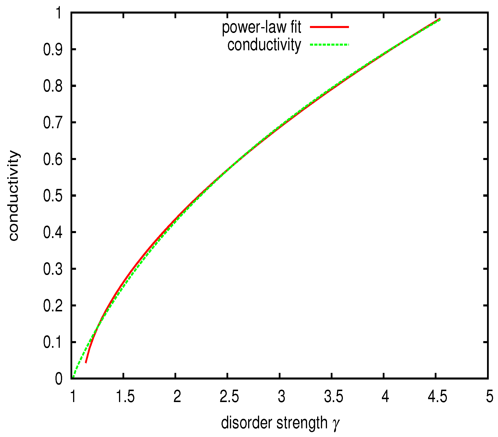
The solution of the self-consistent Equation (10) is inserted into and the conductivity is plotted as a function of disorder strength in Figure 3. The conductivity vanishes linearly with decreasing disorder strength (i.e., with decreasing doping concentration). To illustrate the crossover to a power law with exponent , the calculated conductivity and the power-law fit are plotted together in Figure 4.
5. Discussion and Conclusions
Our result for the DC conductivity in Equation (21), together with the solution of the order parameter in Equation (10), provides a simple description of a metal–insulator transition in doped three-dimensional semiconductors. The metal–insulator transition is characterized by the scattering rate that vanishes in the insulating regime. Such a behavior is not an Anderson transition, since the latter would have a scattering rate on both sides of the transition [38]. Even more important is the change of the coefficient : It is always 1 in the insulating regime and infinite in the metallic regime. This quantity describes the correlations of the Green’s function fluctuations in the relation (18).
There is a linear behavior near the metal–insulator transition and a crossover to a non-critical power law, as depicted in Figure 4. For the linear part the slope of the conductivity is quite robust with respect to the average gap (cf. Figure 3). Away from the transition point a negative curvature appears though, which can be fitted by a power law with exponent (cf. Figure 4). The change of exponents can be related to the discussion in References [33,39] about a crossover of exponents in Si:P from very close to the critical point to further away from . Rosenbaum et al. have found that the conductivity close to the critical point varies from sample to sample [32]. This indicates strong conductivity fluctuations, which may also exist in our random gap model, as indicated by the strong fluctuations of the Green’s functions due to the large values of .
As mentioned in the Introduction, a related metal–insulator transition in three-dimensional Weyl fermionic systems has attracted considerable attention recently [2,3,4,5,6,7,8,9,10,11,12,13,14,15,16,17,18,19,20,21,22,23,24,25,26]. Formally, this transition is very similar, although the underlying Hamiltonian is that of Weyl fermions rather than our simple semi-conductor Hamiltonian in Equation (1). This difference leads to the creation of two distinct insulating phases, characterized by the Hall conductivity in the lower part of the phase diagram in Figure 1 for Weyl fermions. But the role of the particle-hole symmetry, the existence of a massless mode due to spontaneous breaking of this symmetry and the role of diffusion in the metallic phase are the same in both types of models [26,27,28]. This indicates that metal–insulator transitions in systems with particle-hole symmetry are based on the same type of mechanism.
Funding
This research received no external funding.
Acknowledgments
This work was supported by a grant of the Julian Schwinger Foundation.
Conflicts of Interest
The author declares no conflicts of interest.
References
- Ashcroft, N.W.; Mermin, N.D. Solid State Physics; Saunders College: Rochester, NY, USA, 1976. [Google Scholar]
- Fradkin, E. Critical behavior of disordered degenerate semiconductors. I. Models, symmetries, and formalism. Phys. Rev. B 1986, 33, 3257–3262. [Google Scholar] [CrossRef]
- Fradkin, E. Critical behavior of disordered degenerate semiconductors. II. Spectrum and transport properties in mean-field theory. Phys. Rev. B 1986, 33, 3263–3268. [Google Scholar] [CrossRef]
- Wan, X.; Turner, A.M.; Vishwanath, A.; Savrasov, S.Y. Topological semimetal and Fermi-arc surface states in the electronic structure of pyrochlore iridates. Phys. Rev. B 2011, 83, 205101. [Google Scholar] [CrossRef]
- Smith, J.; Banerjee, S.; Pardo, V.; Pickett, W.E. Dirac Point Degenerate with Massive Bands at a Topological Quantum Critical Point. Phys. Rev. Lett. 2011, 106, 056401. [Google Scholar] [CrossRef]
- Burkov, A.A.; Balents, L. Weyl Semimetal in a Topological Insulator Multilayer. Phys. Rev. Lett. 2011, 107, 127205. [Google Scholar] [CrossRef] [Green Version]
- Burkov, A.A.; Hook, M.D.; Balents, L. Topological nodal semimetals. Phys. Rev. B 2011, 84, 235126. [Google Scholar] [CrossRef]
- Xu, G.; Weng, H.; Wang, Z.; Dai, X.; Fang, Z. Chern Semimetal and the Quantized Anomalous Hall Effect in HgCr2Se4. Phys. Rev. Lett. 2011, 107, 186806. [Google Scholar] [CrossRef] [PubMed]
- Witczak-Krempa, W.; Kim, Y.B. Topological and magnetic phases of interacting electrons in the pyrochlore iridates. Phys. Rev. B 2012, 85, 045124. [Google Scholar] [CrossRef]
- Young, S.M.; Zaheer, S.; Teo, J.C.Y.; Kane, C.L.; Mele, E.J.; Rappe, A.M. Dirac Semimetal in Three Dimensions. Phys. Rev. Lett. 2012, 108, 140405. [Google Scholar] [CrossRef] [PubMed]
- Hosur, P.; Parameswaran, S.A.; Vishwanath, A. Charge Transport in Weyl Semimetals. Phys. Rev. Lett. 2012, 108, 046602. [Google Scholar] [CrossRef] [Green Version]
- Wang, Z.; Sun, Y.; Chen, X.-Q.; Franchini, C.; Xu, G.; Weng, H.; Dai, X.; Fang, Z. Dirac semimetal and topological phase transitions in A3Bi (A = Na, K, Rb). Phys. Rev. B 2012, 85, 195320. [Google Scholar] [CrossRef]
- Singh, B.; Sharma, A.; Lin, H.; Hasan, M.Z.; Prasad, R.; Bansil, A. Topological electronic structure and Weyl semimetal in the TlBiSe2 class of semiconductors. Phys. Rev. B 2012, 86, 115208. [Google Scholar] [CrossRef]
- Cho, G.Y. Possible topological phases of bulk magnetically doped Bi2Se3: Turning a topological band insulator into the Weyl semimetal. arXiv 2012, arXiv:1110.1939v2. [Google Scholar]
- Halász, G.B.; Balents, L. Time-reversal invariant realization of the Weyl semimetal phase. Phys. Rev. B 2012, 85, 035103. [Google Scholar] [CrossRef]
- Nandkishore, R.; Huse, D.A.; Sondhi, S. Rare region effects dominate weakly disordered three-dimensional Dirac points. Phys. Rev. B 2014, 89, 245110. [Google Scholar] [CrossRef]
- Liu, C.-X.; Ye, P.; Qi, X.-L. Chiral gauge field and axial anomaly in a Weyl semimetal. Phys. Rev. B 2013, 87, 235306. [Google Scholar] [CrossRef]
- Biswas, R.R.; Ryu, S. Diffusive transport in Weyl semimetals. Phys. Rev. B 2014, 89, 014205. [Google Scholar] [CrossRef]
- Kobayashi, K.; Ohtsuki, T.; Imura, K.-I. Disordered Weak and Strong Topological Insulators. Phys. Rev. Lett. 2013, 110, 236803. [Google Scholar] [CrossRef] [Green Version]
- Huang, Z.; Das, T.; Balatsky, A.V.; Arovas, D.P. Stability of Weyl metals under impurity scattering. Phys. Rev. B 2013, 87, 155123. [Google Scholar] [CrossRef]
- Kobayashi, K.; Ohtsuki, T.; Imura, K.-I.; Herbut, I.F. Density of States Scaling at the Semimetal to Metal Transition in Three Dimensional Topological Insulators. Phys. Rev. Lett. 2014, 112, 016402. [Google Scholar] [CrossRef] [Green Version]
- Ominato, Y.; Koshino, M. Quantum transport in a three-dimensional Weyl electron system. Phys. Rev. B 2014, 89, 054202. [Google Scholar] [CrossRef]
- Roy, B.; Das Sarma, S. Diffusive quantum criticality in three-dimensional disordered Dirac semimetals. Phys. Rev. B 2014, 90, 241112(R). [Google Scholar] [CrossRef]
- Sbierski, B.; Pohl, G.; Bergholtz, E.J.; Brouwer, P.W. Quantum Transport of Disordered Weyl Semimetals at the Nodal Point. Phys. Rev. Lett. 2014, 113, 026602. [Google Scholar] [CrossRef] [PubMed] [Green Version]
- Syzranov, S.V.; Gurarie, V.; Radzihovy, L. Critical Transport in Weakly Disordered Semiconductors and Semimetals. Phys. Rev. Lett. 2015, 114, 166601. [Google Scholar] [CrossRef] [Green Version]
- Ziegler, K. Quantum transport in 3D Weyl semimetals: Is there a metal-insulator transition? Eur. Phys. J. B 2016, 89, 268. [Google Scholar] [CrossRef] [Green Version]
- Ziegler, K. Quantum transport with strong scattering: beyond the nonlinear sigma model. J. Phys. A Math. Theor. 2015, 48, 055102. [Google Scholar] [CrossRef]
- Ziegler, K. Zero mode protection at particle-hole symmetry: A geometric interpretation. J. Phys. A Math. Theor. 2019, 52, 455101. [Google Scholar] [CrossRef]
- Rosenbaum, T.F.; Andres, K.; Thomas, G.A.; Bhatt, R.N. Sharp Metal-Insulator Transition in a Random Solid. Phys. Rev. Lett. 1980, 45, 1723–1726. [Google Scholar] [CrossRef]
- Rosenbaum, T.F.; Milligan, R.F.; Paalanen, M.A.; Thomas, G.A.; Bhatt, R.N.; Lin, W. Metal-insulator transition in a doped semiconductor. Phys. Rev. B 1983, 27, 7509–7523. [Google Scholar] [CrossRef] [Green Version]
- Roy, A.; Sarachik, M.P. Susceptibility of Si:P across the metal-insulator transition. II. Evidence for local moments in the metallic phase. Phys. Rev. B 1988, 37, 5531–5534. [Google Scholar] [CrossRef]
- Rosenbaum, T.F.; Thomas, G.A.; Paalanen, M.A. Critical behavior of Si:P at the metal-insulator transition. Phys. Rev. Lett. 1994, 72, 2121. [Google Scholar] [CrossRef] [PubMed]
- Löhneysen, H. Current issues in the physics of heavily doped semiconductors at the metal-insulator transition. Philos. Trans. R. Soc. Lond. A 1998, 356, 139–156. [Google Scholar] [CrossRef]
- Ziegler, K. Scaling behavior and universality near the quantum Hall transition. Phys. Rev. B 1997, 55, 10661–10670. [Google Scholar] [CrossRef] [Green Version]
- Ziegler, K. Random-Gap Model for Graphene and Graphene Bilayers. Phys. Rev. Lett. 2009, 102, 126802. [Google Scholar] [CrossRef] [PubMed] [Green Version]
- Altshuler, B.L.; Simons, B.D. Mesoscopic Quantum Physics; Akkermans, E., Montambaux, G., Pichard, J.-L., Zinn-Justin, J., Eds.; North-Holland: Amsterdam, The Netherlands, 1995. [Google Scholar]
- Altland, A.; Simons, B.D. Condensed Matter Field Theory; Cambridge University Press: Cambridge, MA, USA, 2010. [Google Scholar]
- Schäfer, L.; Wegner, F. Disordered system with n orbitals per site: Lagrange formulation, hyperbolic symmetry, and goldstone modes. Z. Phys. B 1980, 38, 113–126. [Google Scholar] [CrossRef]
- Stupp, H.; Hornung, M.; Lakner, M.; Madel, O.; Löhneysen, H. Possible solution of the conductivity exponent puzzle for the metal-insulator transition in heavily doped uncompensated semiconductors. Phys. Rev. Lett. 1993, 71, 2634–2637. [Google Scholar] [CrossRef]
Figure 1.
Phase diagram of the metal–insulator transition of the three-dimensional random gap model from Equation (11), where disorder is the parameter and the average gap is .
Figure 1.
Phase diagram of the metal–insulator transition of the three-dimensional random gap model from Equation (11), where disorder is the parameter and the average gap is .
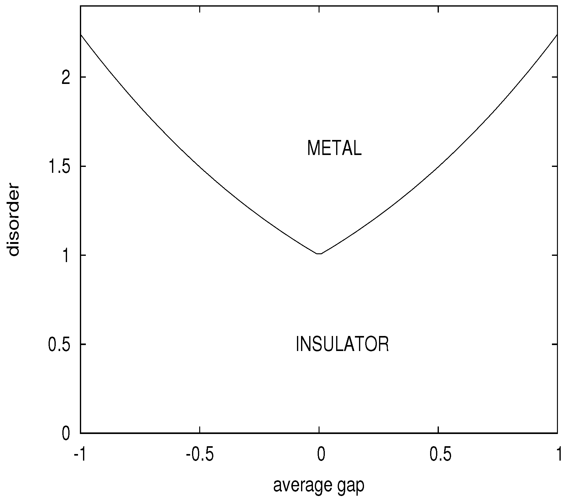
Figure 2.
Average density of states of the three-dimensional random gap model for fixed and average gap (full curve) and (dashed curve).
Figure 2.
Average density of states of the three-dimensional random gap model for fixed and average gap (full curve) and (dashed curve).
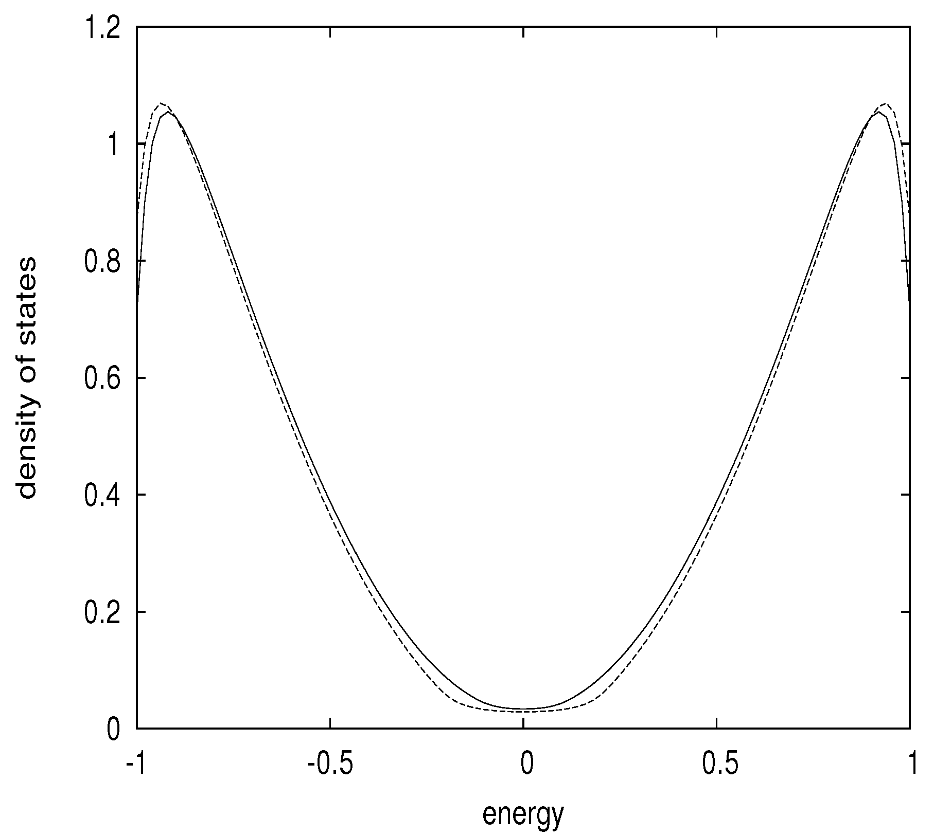
Figure 3.
Conductivity as a function of disorder for an average gap (red curve), (green curve) and (blue curve). There is a metal–insulator transition at , at and at , respectively.
Figure 3.
Conductivity as a function of disorder for an average gap (red curve), (green curve) and (blue curve). There is a metal–insulator transition at , at and at , respectively.
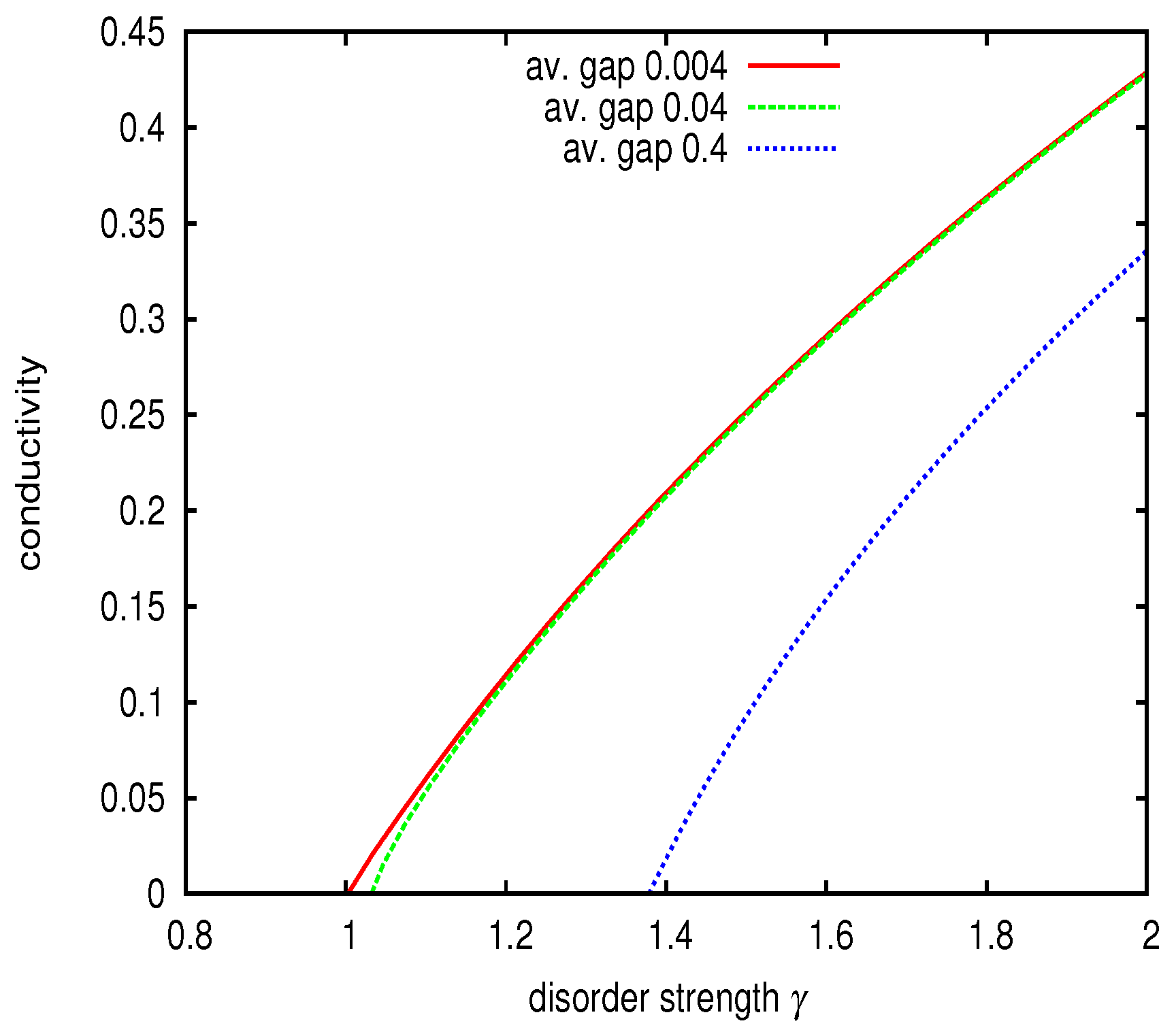
Figure 4.
This plot demonstrates the crossover in the critical regime of the conductivity (green curve) through the fitting (red) curve . The latter fits the conductivity very well away from the critical point for .
Figure 4.
This plot demonstrates the crossover in the critical regime of the conductivity (green curve) through the fitting (red) curve . The latter fits the conductivity very well away from the critical point for .
© 2019 by the author. Licensee MDPI, Basel, Switzerland. This article is an open access article distributed under the terms and conditions of the Creative Commons Attribution (CC BY) license (http://creativecommons.org/licenses/by/4.0/).
Share and Cite
MDPI and ACS Style
Ziegler, K. Metal–Insulator Transition in Three-Dimensional Semiconductors. Symmetry 2019, 11, 1345. https://doi.org/10.3390/sym11111345
AMA Style
Ziegler K. Metal–Insulator Transition in Three-Dimensional Semiconductors. Symmetry. 2019; 11(11):1345. https://doi.org/10.3390/sym11111345
Chicago/Turabian StyleZiegler, Klaus. 2019. "Metal–Insulator Transition in Three-Dimensional Semiconductors" Symmetry 11, no. 11: 1345. https://doi.org/10.3390/sym11111345
Note that from the first issue of 2016, this journal uses article numbers instead of page numbers. See further details here.