Lithographic Performance of Aryl Epoxy Thermoset Resins as Negative Tone Photoresist for Microlithography


Abstract

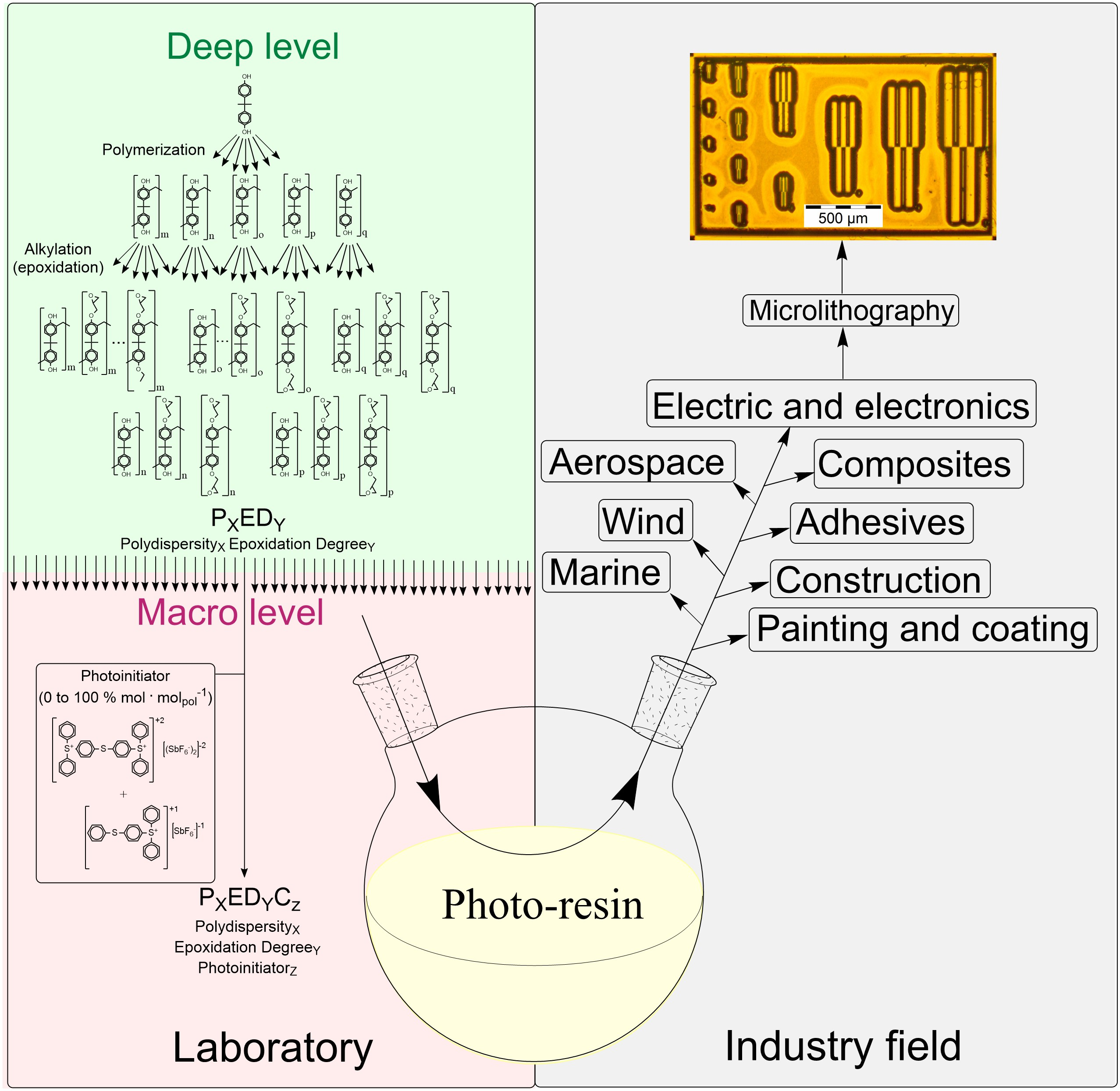
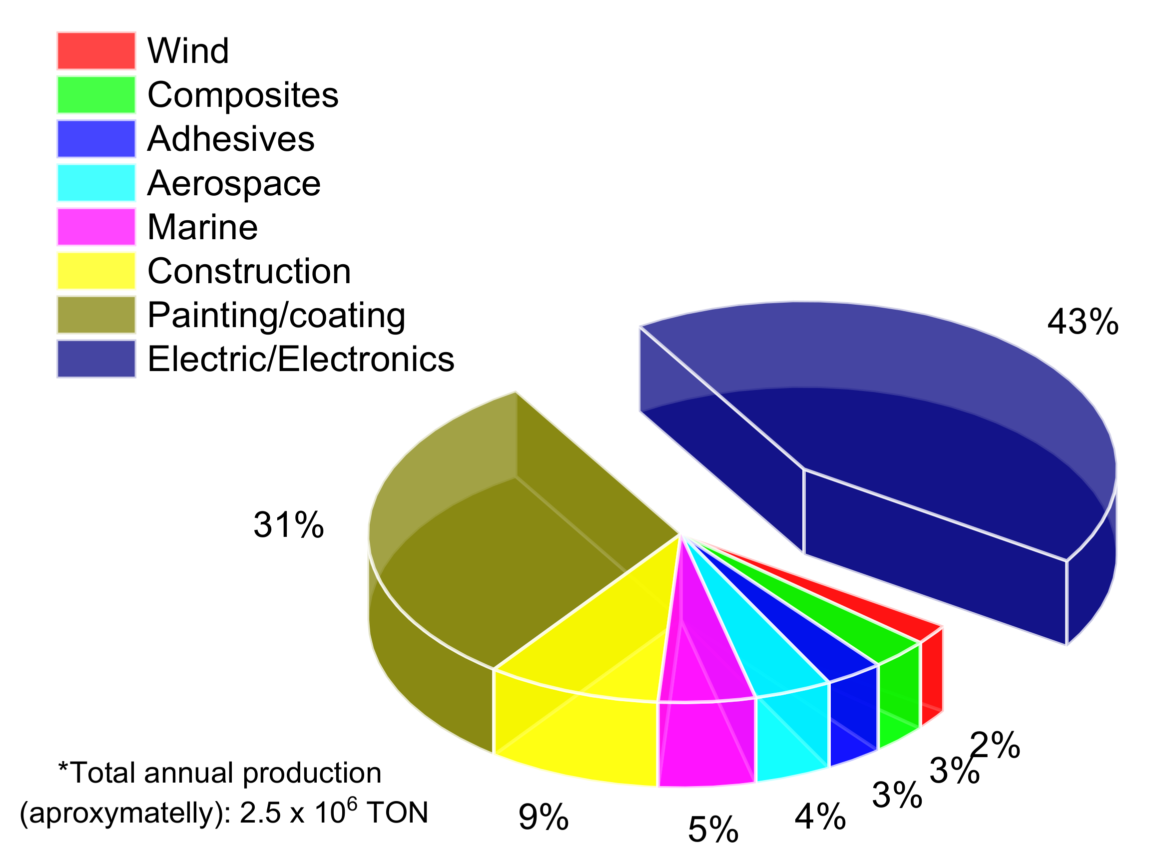
1. Introduction
2. Materials and Methods
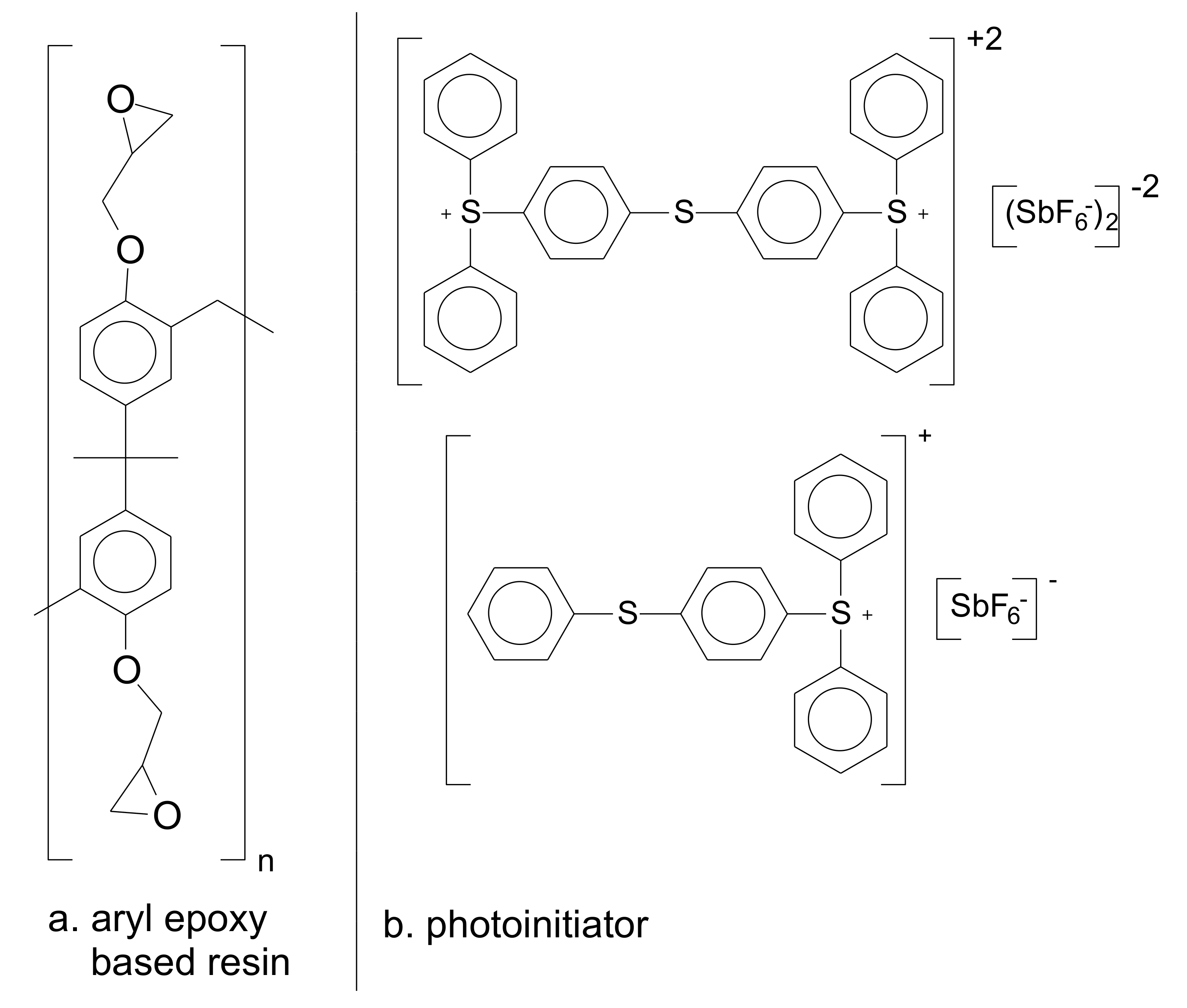
2.1. Materials
2.2. Methods
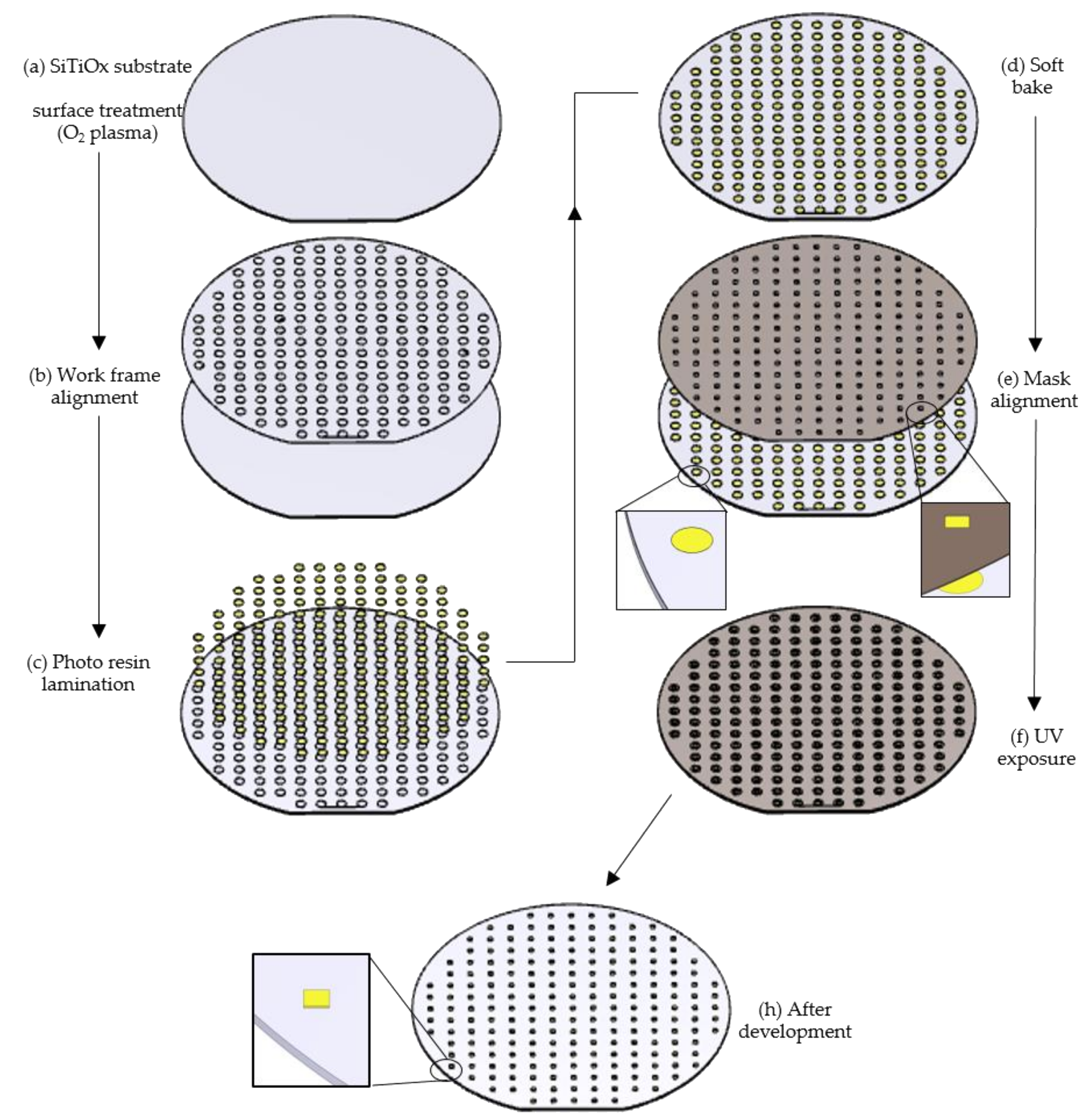
2.2.1. Quality Evaluation Using UV Lithography
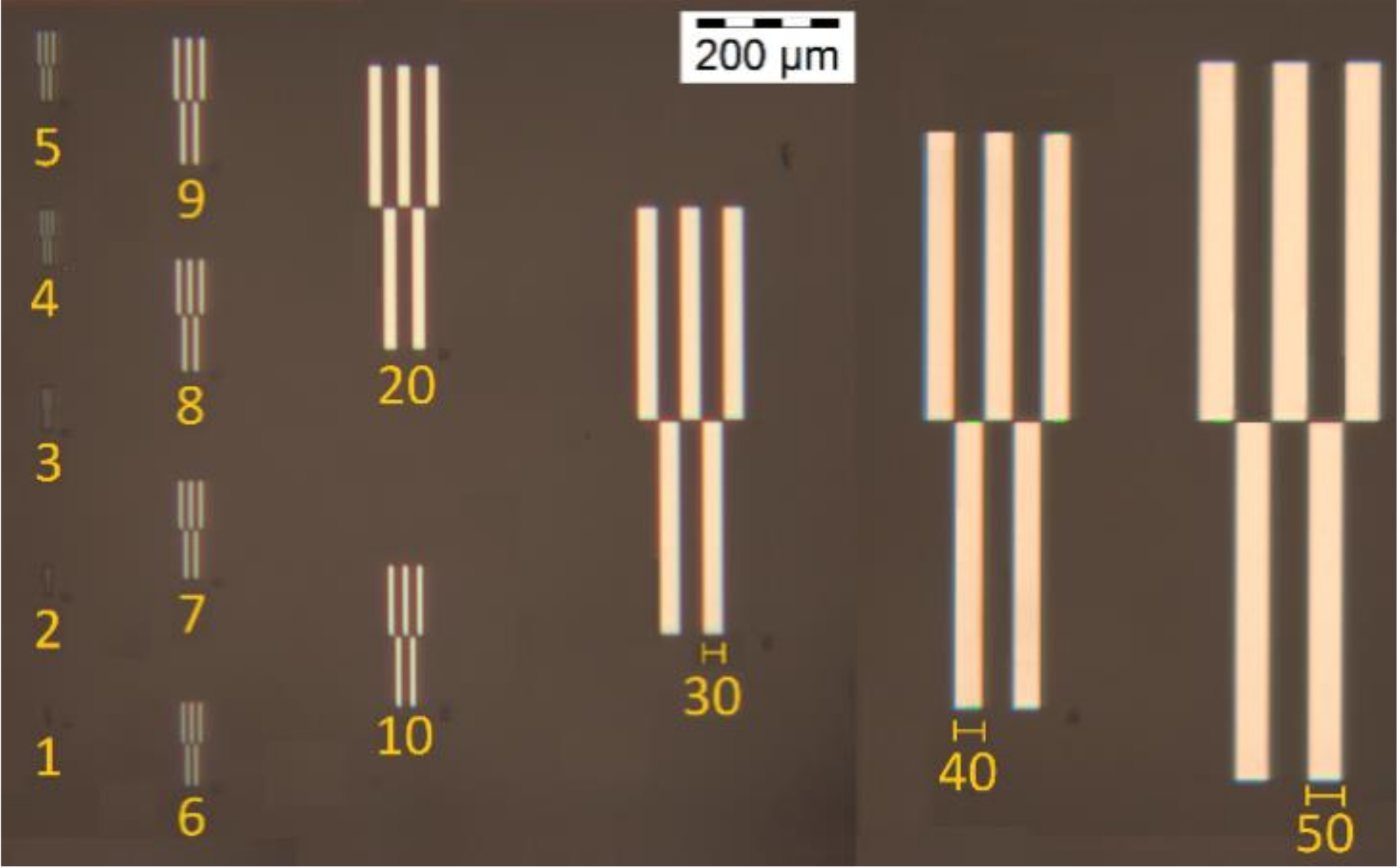
2.2.2. Test Pattern Structures Using Deep-UV and UV Lithography
2.2.3. Plasma Etching
2.2.4. Spin-Coating
2.2.5. Deep-UV and UV Lithography Exposures
2.2.6. Scanning Electron Microscopy (SEM)
2.2.7. Optical Microscope Measurements
3. Results and Discussion
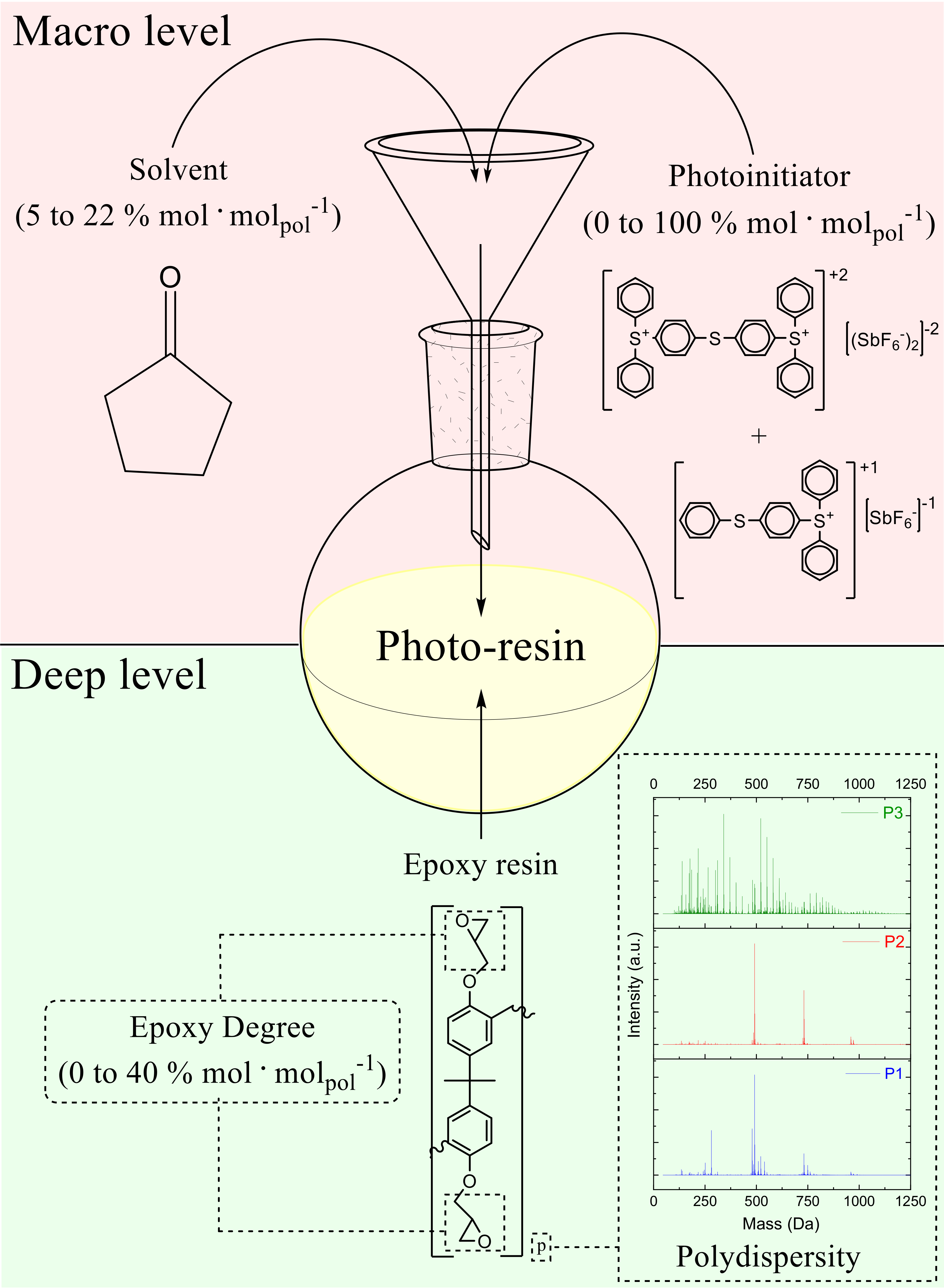
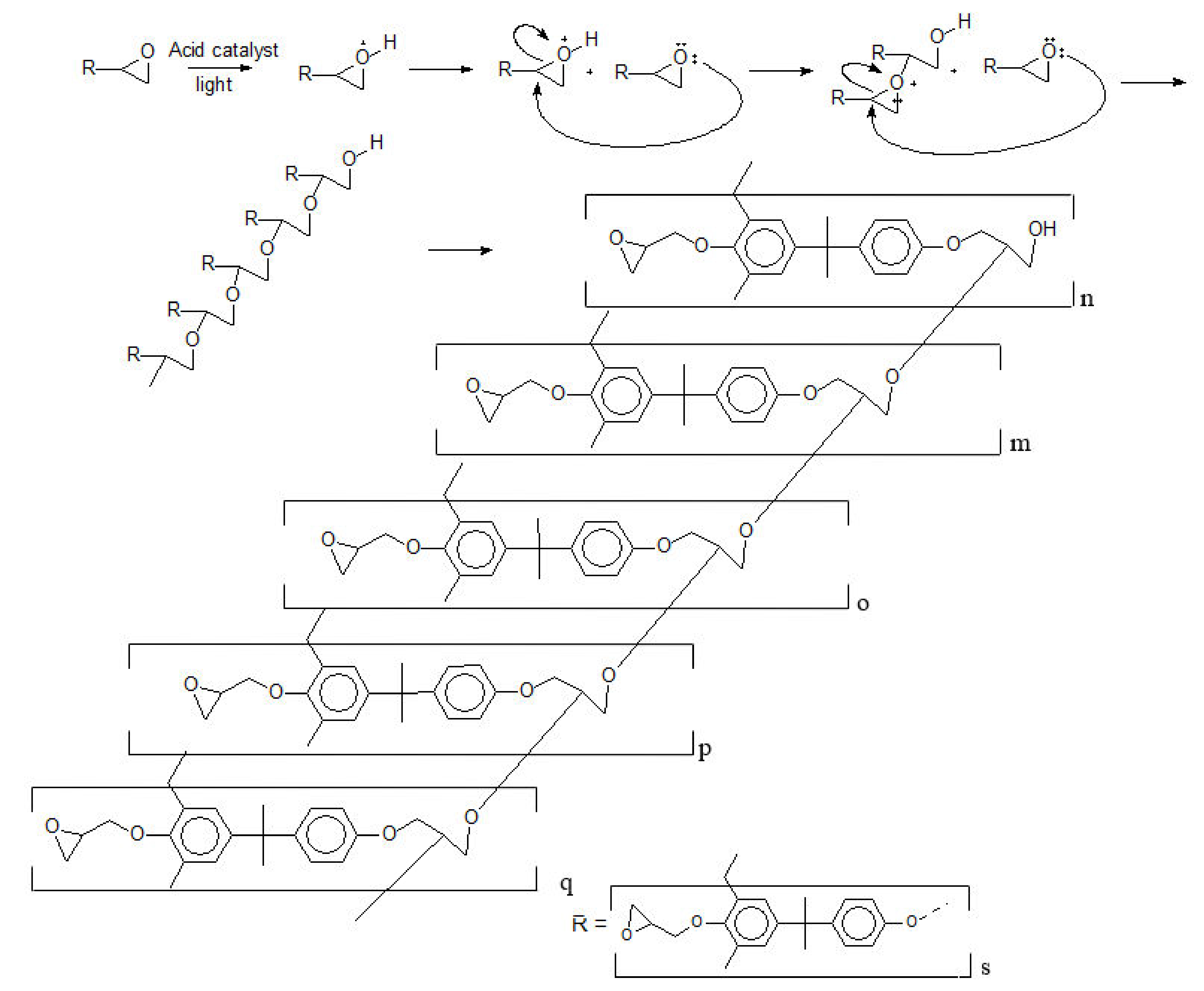
3.1. Formulation of the Photo-Resins
- ED: epoxidation degree
- C: photoinitiator
- x: type of resin
- y: the amount of epoxy groups
- z: the amount of catalyst
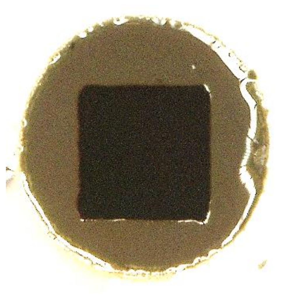
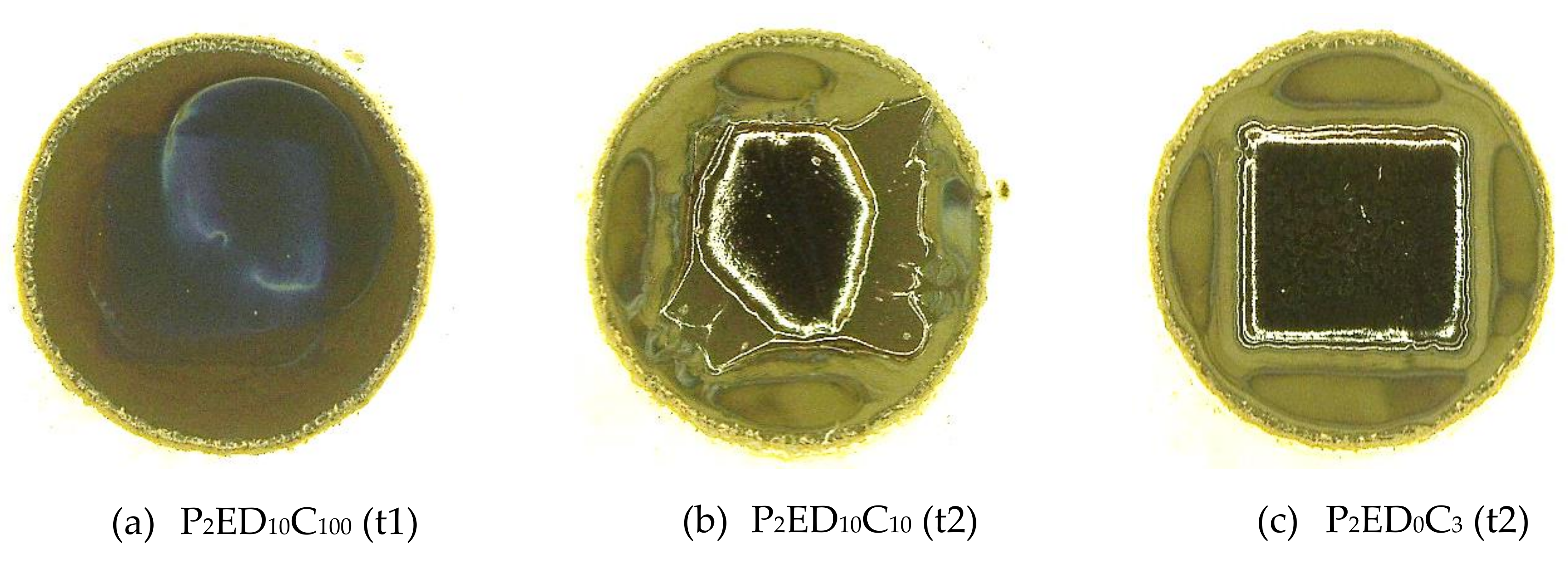
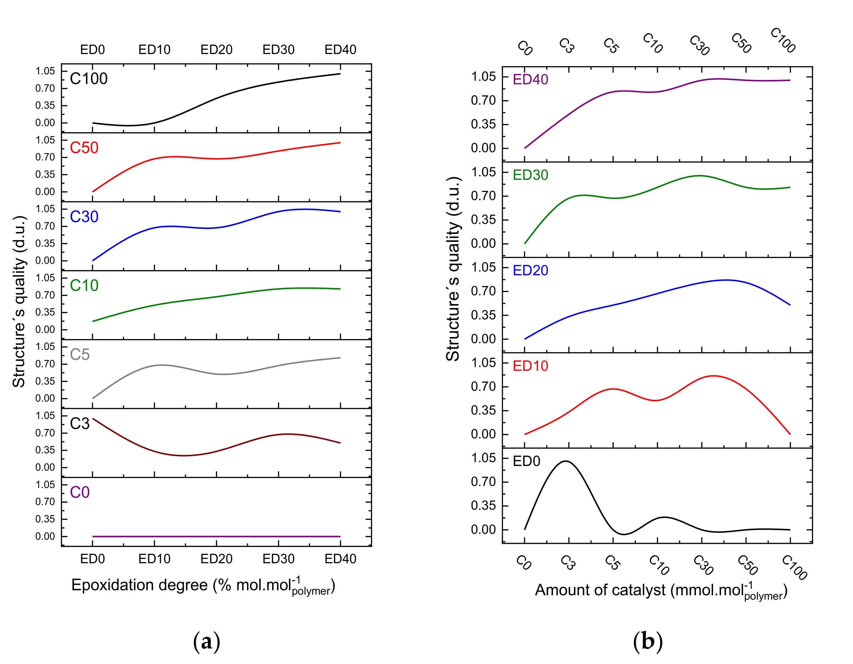
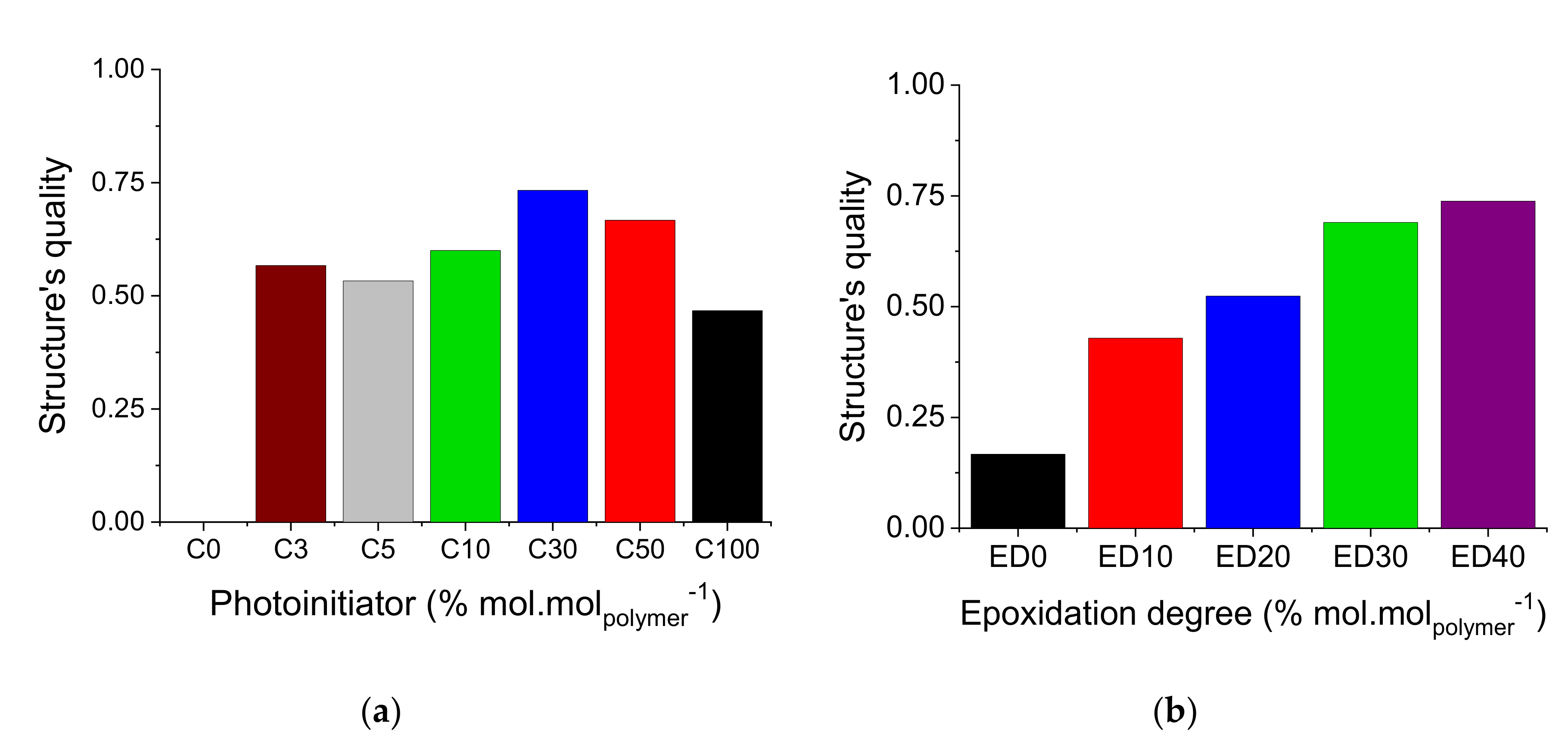
3.2. Quality Evaluation of the Photo-Resins
- 0 value for the not remained structure after the development step (complete lift-off);
- 0.5 value for remained structures with defects after the development;
- 1.0 value for entirely remained structures after the development.
- (1)
- The photoinitiator is a Lewis acid, releasing a proton to the reaction medium;
- (2)
- The oligomers (Poly(2,2-Bis(4-hydroxyphenyl)propane)) have no secondary products and termination groups [10];
- (3)
- All the epoxy rings are intact, and there is no epoxy derivate [10]; and
- (4)
- The epoxidation degree of poly(2,2-Bis(4-hydroxyphenyl)propane) is 100%.
- (1)
- The polydispersity of the photo-resins shall be considered in crosslinking mechanism; and
- (2)
- The crosslinking efficiency (irradiation step) tend to be improved if the oligomer chains present less secondary and derivative products.
4. Conclusions
- (1)
- For large structures (roughly above 1 mm2), the tuning of the deep and macro levels of properties can be less restricted;
- (2)
- For structures under 50 µm it is necessary to consider a specific polydispersion profile of the photo-resin to achieve better quality in the structures (deep level of properties). It is also suggested to restrict the concentrations for the epoxidation degree (deep level of properties), and photoinitiator (macro level of properties).
Supplementary Materials
Author Contributions
Funding
Acknowledgments
Conflicts of Interest
References
- Turner, S.R.; Daly, R.C. 7 - Photochemical and Radiation Sensitive Resists. In Comprehensive Polymer Science and Supplements; Allen, G., Bevington, J.C., Eds.; Pergamon: Amsterdam, The Netherlands, 1989; pp. 193–225. [Google Scholar] [CrossRef]
- Willson, C.; Dammel, R.; Reiser, A. Photoresist materials: A historical perspective. Proc. Spie Int. Soc. Opt. Eng. 1997, 3050. [Google Scholar] [CrossRef]
- Jiguet, S.; Bertsch, A.; Judelewicz, M.; Hofmann, H.; Renaud, P. SU-8 nanocomposite photoresist with low stress properties for microfabrication applications. Microelectron. Eng. 2006, 83, 1966–1970. [Google Scholar] [CrossRef]
- O’Brien, J.; Hughes, P.J.; Brunet, M.; O’Neill, B.; Alderman, J.; Lane, B.; O’Riordan, A.; O’Driscoll, C. Advanced photoresist technologies for microsystems. J. Micromech. Microeng. 2001, 11, 353. [Google Scholar] [CrossRef]
- Vlnieska, V.; Zakharova, M.; Börner, M.; Bade, K.; Mohr, J.; Kunka, D. Chemical and Molecular Variations in Commercial Epoxide Photoresists for X-ray Lithography. Appl. Sci. 2018, 8, 528. [Google Scholar] [CrossRef]
- Chiamori, H.C.; Brown, J.W.; Adhiprakasha, E.V.; Hantsoo, E.T.; Straalsund, J.B.; Melosh, N.A.; Pruitt, B.L. Suspension of nanoparticles in SU-8: Processing and characterization of nanocomposite polymers. Microelectron. J. 2008, 39, 228–236. [Google Scholar] [CrossRef]
- Tung, K.K.; Wong, W.H.; Pun, E.Y.B. Polymeric optical waveguides using direct ultraviolet photolithography process. Appl. Phys. A 2005, 80, 621–626. [Google Scholar] [CrossRef]
- Lorenz, H.; Despont, M.; Fahrni, N.; Brugger, J.; Vettiger, P.; Renaud, P. High-aspect-ratio, ultrathick, negative-tone near-UV photoresist and its applications for MEMS. Sens. Actuators A Phys. 1998, 64, 33–39. [Google Scholar] [CrossRef]
- Mustata, F.; Tudorachi, N.; Bicu, I. The kinetic study and thermal characterization of epoxy resins crosslinked with amino carboxylic acids. J. Anal. Appl. Pyrolysis 2015, 112, 180–191. [Google Scholar] [CrossRef]
- Vlnieska, V.; Mikhaylov, A.; Zakharova, M.; Blasco, E.; Kunka, D. Epoxy Resins for Negative Tone Photoresists. Polymers 2019, 11, 1457. [Google Scholar] [CrossRef]
- Organisation for Economic Co-operation and Development (OECD). Photoresist Use in Semiconductor Manufacturing. In Series on Emission Scenario Documents, No. 9. Available online: https://read.oecd-ilibrary.org/environment/photoresist-use-in-semiconductor-manufacturing_9789264221161-en#page1 (accessed on 1 October 2020).
- Plastics Europe. Annual Report. 2018. Available online: https://www.plasticseurope.org/en/resources/publications/498-plasticseurope-annual-review-2017-2018 (accessed on 11 October 2020).
- McKeen, L. 13 - Elastomers. In The Effect of Sterilization on Plastics and Elastomers (Third Edition); McKeen, L., Ed.; William Andrew Publishing: Boston, MA, USA, 2012; pp. 319–353. [Google Scholar] [CrossRef]
- Zakharova, M.; Vlnieska, V.; Fornasier, H.; Börner, M.; Rolo, T.d.S.; Mohr, J.; Kunka, D. Development and Characterization of Two-Dimensional Gratings for Single-Shot X-ray Phase-Contrast Imaging. Appl. Sci. 2018, 8, 468. [Google Scholar] [CrossRef]
- Shipley. Microposit S1800 Series Photo Resists Data Sheet. Available online: https://amolf.nl/wp-content/uploads/2016/09/datasheets_S1800.pdf (accessed on 2 October 2020).
- Microchem, K. SU-8 3000 Photoresist Data Sheet. Available online: https://kayakuam.com/wp-content/uploads/2019/09/SU-8-3000-Data-Sheet.pdf (accessed on 2 October 2020).
- Johnson, D.; Goettert, J.; Singh, V.; Johnson, D. SUEX Dry Film Resist Data Sheet. Available online: https://www.lsu.edu/camd/files/DJ_AR2012_SUEXoverview.pdf (accessed on 2 October 2020).


| Level of Formulation | Compound | Range (% mol·molpolymer−1) |
|---|---|---|
| Deep level (oligomer composition) | Profile of Resin (polydispersity) | P1, P2, P3 |
| Epoxidation degree | 0; 10; 20; 30; 40 | |
| Macro level (added chemicals to the formulation) | Photoinitiator | 0; 3; 5; 10; 30; 50; 100 |
| Solvent | 0–22 * |
| P1ED40C30 | P2ED40C30 | P3ED40C30 | |
|---|---|---|---|
| Polydispersity (Mass spectroscopy) |  |  |  |
| Optical microscopy (UVL) |  |  |  |
| Optical microscopy (DUVL) |  |  |  |
| Scanning electron microscopy (UVL) |  |  |  |
Publisher’s Note: MDPI stays neutral with regard to jurisdictional claims in published maps and institutional affiliations. |
© 2020 by the authors. Licensee MDPI, Basel, Switzerland. This article is an open access article distributed under the terms and conditions of the Creative Commons Attribution (CC BY) license (http://creativecommons.org/licenses/by/4.0/).
Share and Cite
Vlnieska, V.; Zakharova, M.; Mikhaylov, A.; Kunka, D. Lithographic Performance of Aryl Epoxy Thermoset Resins as Negative Tone Photoresist for Microlithography. Polymers 2020, 12, 2359. https://doi.org/10.3390/polym12102359
Vlnieska V, Zakharova M, Mikhaylov A, Kunka D. Lithographic Performance of Aryl Epoxy Thermoset Resins as Negative Tone Photoresist for Microlithography. Polymers. 2020; 12(10):2359. https://doi.org/10.3390/polym12102359
Chicago/Turabian StyleVlnieska, Vitor, Margarita Zakharova, Andrey Mikhaylov, and Danays Kunka. 2020. "Lithographic Performance of Aryl Epoxy Thermoset Resins as Negative Tone Photoresist for Microlithography" Polymers 12, no. 10: 2359. https://doi.org/10.3390/polym12102359
APA StyleVlnieska, V., Zakharova, M., Mikhaylov, A., & Kunka, D. (2020). Lithographic Performance of Aryl Epoxy Thermoset Resins as Negative Tone Photoresist for Microlithography. Polymers, 12(10), 2359. https://doi.org/10.3390/polym12102359