1. Introduction
Owing to its many advantages over silicon, silicon carbide (SiC), in particularly its 4H polytype, is becoming a mainstream material for the industry of high-power electronics. Due to its wide bandgap, radiation hardness, high breakdown field, and high melting point, SiC is also a promising semiconductor for the fabrication of nuclear radiation detectors working in harsh environments. SiC diodes for radiation detection are highly sensitive to defects that introduce deep levels which act as recombination centers and therefore degrade carrier lifetimes.
The majority carrier traps in both
n- and
p-type 4H–SiC, and their respective deep levels, have been extensively studied by deep-level transient spectroscopy (DLTS) for decades. The main recombination center in
n-type 4H–SiC is known as Z
1/2 and it has been identified as a (=/0) transition from the single carbon vacancy (V
C) [
1].
Contrary to majority carrier traps, minority carrier traps in 4H–SiC are still far from fully exploited. A short list of studies on minority carrier traps in as-grown, electron-irradiated, and thermally oxidized 4H–SiC [
2,
3,
4,
5] has been reported in the literature.
Minority carriers in Schottky barrier diodes (SBDs) could be optically generated by use of above-bandgap light [
6]. The first experimental application of the generation of minority carriers by use of a light with an energy just above the bandgap energy as a technique for manipulating the occupancy of deep states was described by Hamilton et al. [
7] and it was called the minority carrier capture (MCC) method. It was further developed into minority carrier transient spectroscopy (MCTS) by Brunwin et al. [
8]. In addition to MCTS, a technique called optical-DLTS, in which the employed light has an energy below the bandgap energy, has been reported [
6].
The MCTS technique offers unique opportunities for studying the minority carrier traps in SBDs, which are beyond the reach of more known and well-used techniques such as DLTS. However, the studies by means of MCTS and Laplace-MCTS are still very rare in the literature.
In this work, we present results on a minority carrier trap in n-type 4H–SiC SBDs obtained by MCTS and high-resolution Laplace-MCTS. In order to carry out the complete electrical characterization of deep levels, it is necessary to complement DLTS measurements with MCTS measurements. Recombination via the deep level can be assessed from the energy and hole capture cross-section () measured by the MCTS technique. The characterization of minority carrier capture is crucial as carrier trapping and recombination strongly affect 4H–SiC device characteristics. Charge collection efficiency and energy resolution of 4H–SiC detectors are determined by these processes.
2. Experimental Details
n-type SiC SBDs were produced on nitrogen-doped (up to 4.5 × 10
14 cm
−3), epitaxially grown 4H–SiC single-crystal layers, approximately 25 µm thick [
9]. The Schottky barriers for conventional DLTS measurements were formed by the evaporation of nickel through a metal mask with patterned square apertures of 1 × 1 mm, while ohmic contacts were formed on the backside of the SiC substrate by nickel sintering at 950 °C in an Ar atmosphere. More details about the SBD fabrication are given elsewhere [
10].
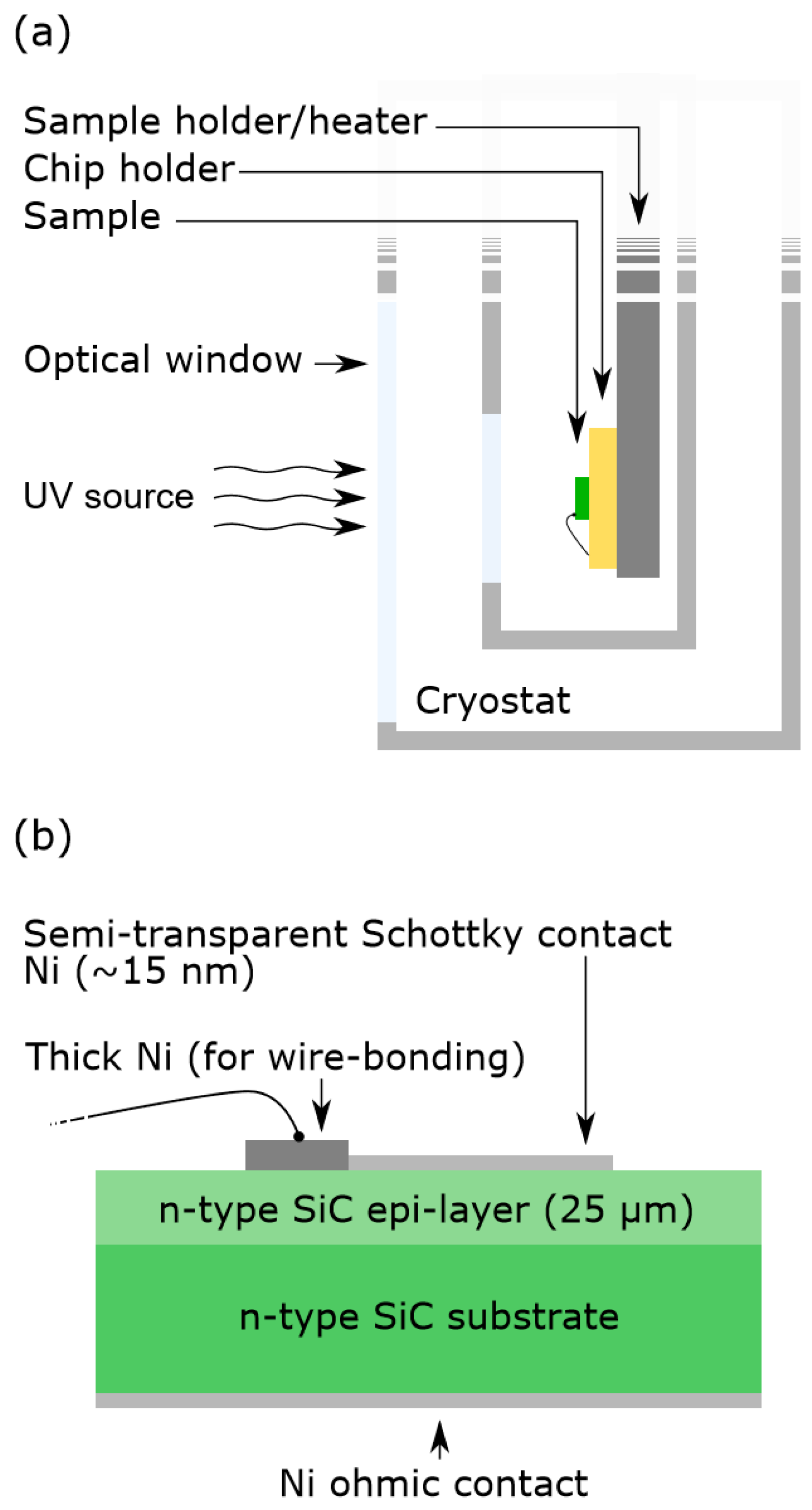
Semi-transparent SBDs for MCTS measurements were formed by the evaporation of a thin film of nickel through a metal mask with apertures of 2 × 2 mm. The thickness was measured to be 15 nm. For wire bonding of the front contact, a thick film of nickel (1 × 1 mm) was stacked on one corner of the thin film.
The quality of the SBDs was investigated by current–voltage (I–V) and capacitance–voltage (C–V) measurements. Majority carrier traps were analyzed by means of conventional DLTS and minority carrier traps were measured by MCTS and Laplace-MCTS
Figure 1 shows schematic representation of the experimental setup (
Figure 1a) and the semi-transparent
n-type 4H–SiC Schottky barrier diode (
Figure 1b).
MCTS and Laplace-MCTS measurements were carried out using an experimental set up consisting of Boonton 7200 capacitance meter and NI PCI-6251 DAQ. For optical excitation, a 265 nm LED (ThorLabs M265L3 LED) with a Thorlabs DC2200 LED driver was used
To study the minority carrier capture kinetics, capacitance transients were measured by varying the optical pulse widths from 100 µs up to 50 ms.
The sampling rate, number of samples, and the number of averaged scans during the Laplace-MCTS measurements were in the range of 6–11 Hz, 3 × 10⁴, and 100–400, respectively. Reverse bias was constant during the MCTS/Laplace-MCTS measurements; it was −10 V for all cases.
3. Result and Discussion
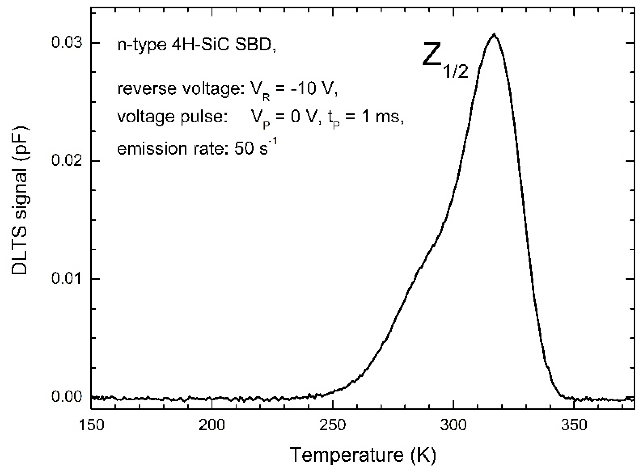
Figure 2 shows the DLTS spectrum for the as-grown
n-type 4H–SiC SBD. One dominant peak with the peak maximum at around 320 K was present. This peak known as Z
1/2 is ascribed to (=/0) transition from the single carbon vacancy (V
C) in 4H–SiC and has been extensively studied in the past decades [
1,
11,
12]. It is usually present in the as-grown material in concentrations in the range of 10
12–10
13 cm
−3. The estimated concentration of Z
1/2 defect in our samples was 1.7 × 10
12 cm
−3.
Recently, we provided direct evidence that the broad Z
1/2 peak has two components, namely Z
1 and Z
2, with activation energies for electron emission of 0.59 and 0.67 eV, respectively. We assigned these components to (=/0) transition sequences from negative-
U ordered acceptor levels of carbon vacancy (V
C) defects at hexagonal and pseudo-cubic sites, respectively [
12].
Due to the favorable electrical properties and with respect to possible device applications, n-type 4H–SiC is the most studied SiC polytype. Consequently, much more information regarding the electrical activity of majority carrier traps is available, as compared to minority carrier traps.
In order to obtain new information regarding the minority carrier traps in
n-type 4H–SiC SBDs, we applied the MCTS technique (
Figure 1). A constant reverse bias of −10 V was maintained during the measurements, while optical excitation pulses were applied using the 265 nm LED light through the semi-transparent front contact.
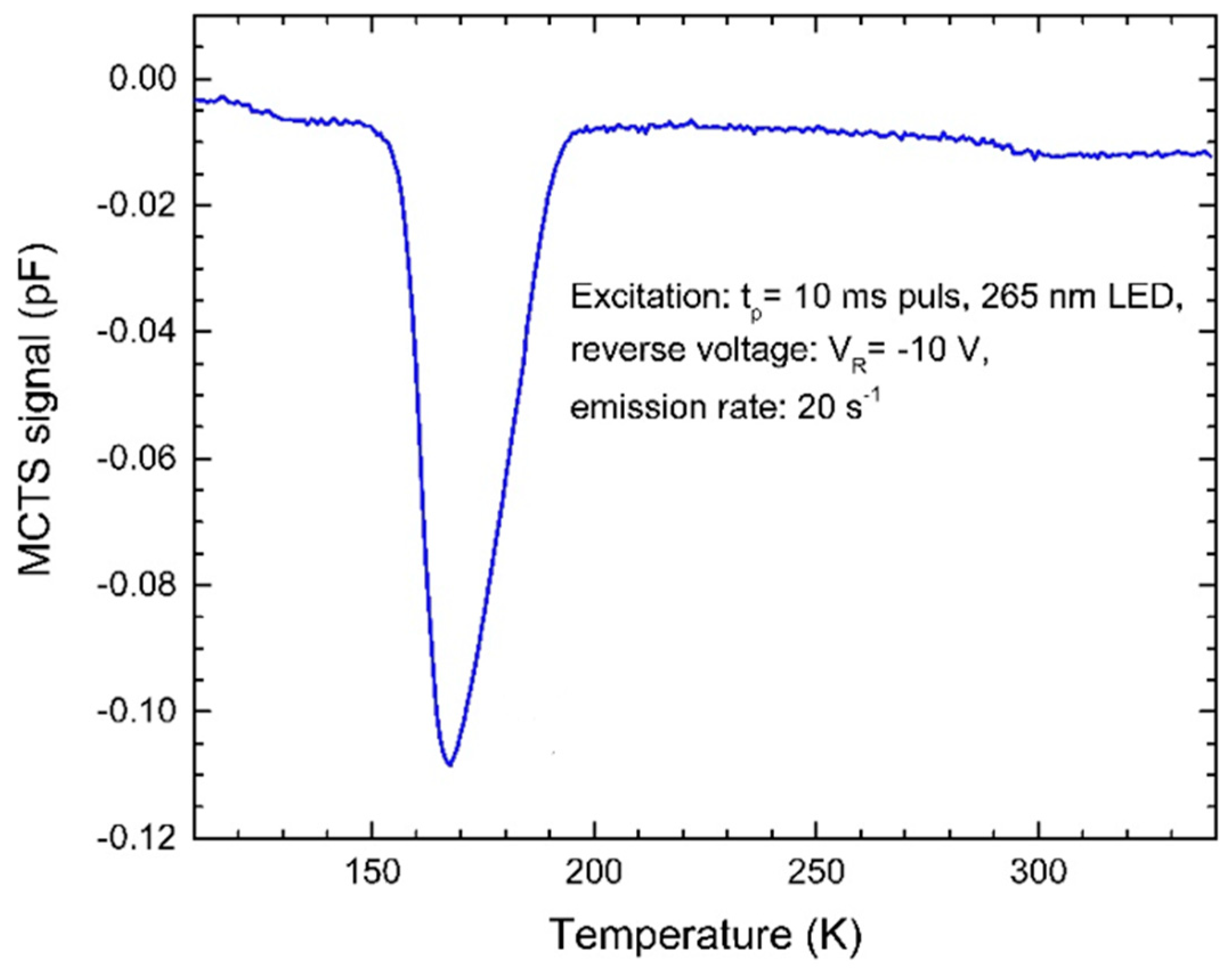
Figure 3 shows the MCTS spectrum for the as-grown
n-type 4H–SiC SBD. One peak with its maximum at around 170 K was present.
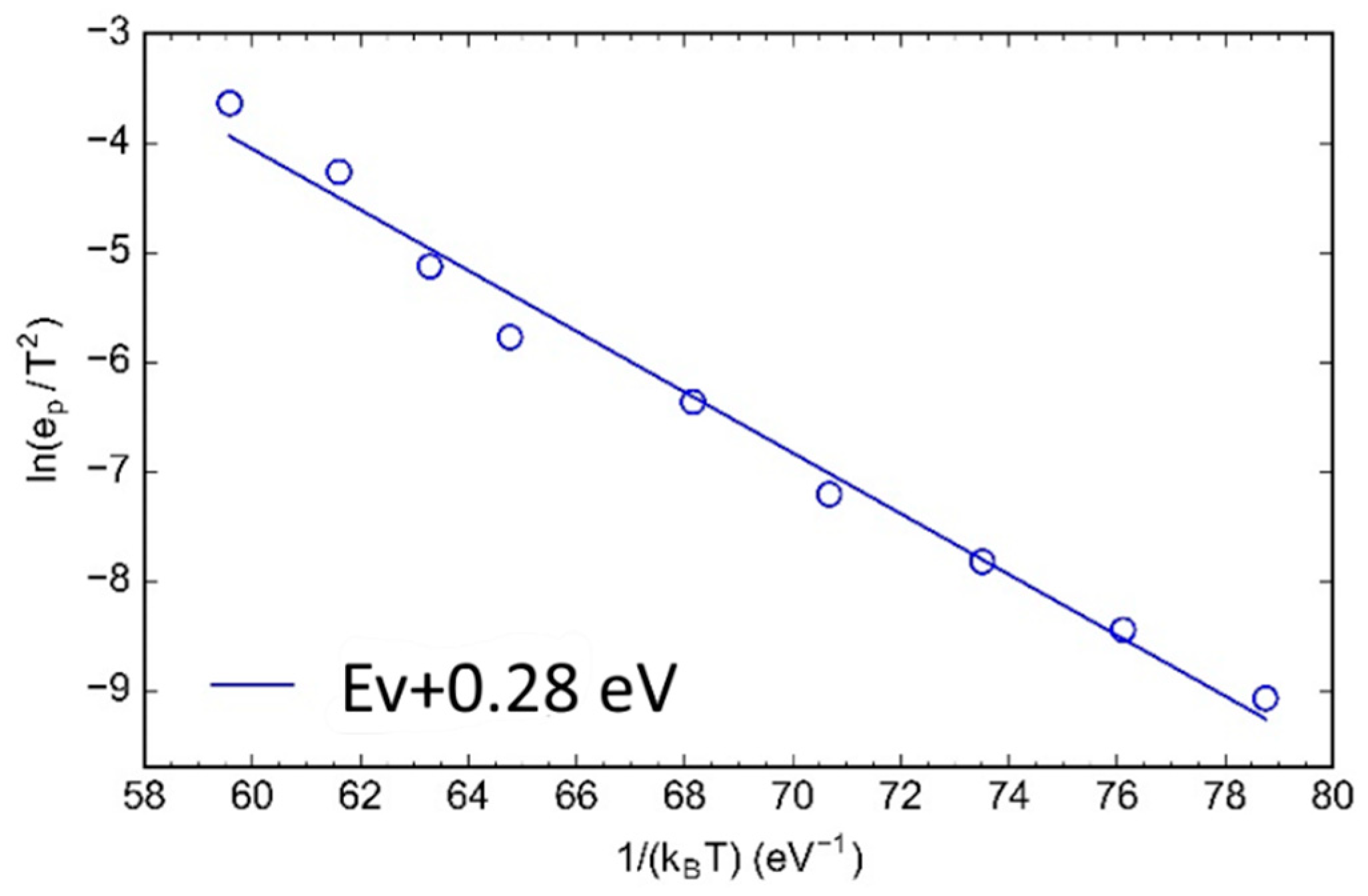
From the Arrhenius graph for the activation energy for hole emission, we estimated the energy level position for this minority trap to be
Ev + 0.28 eV (
Figure 4).
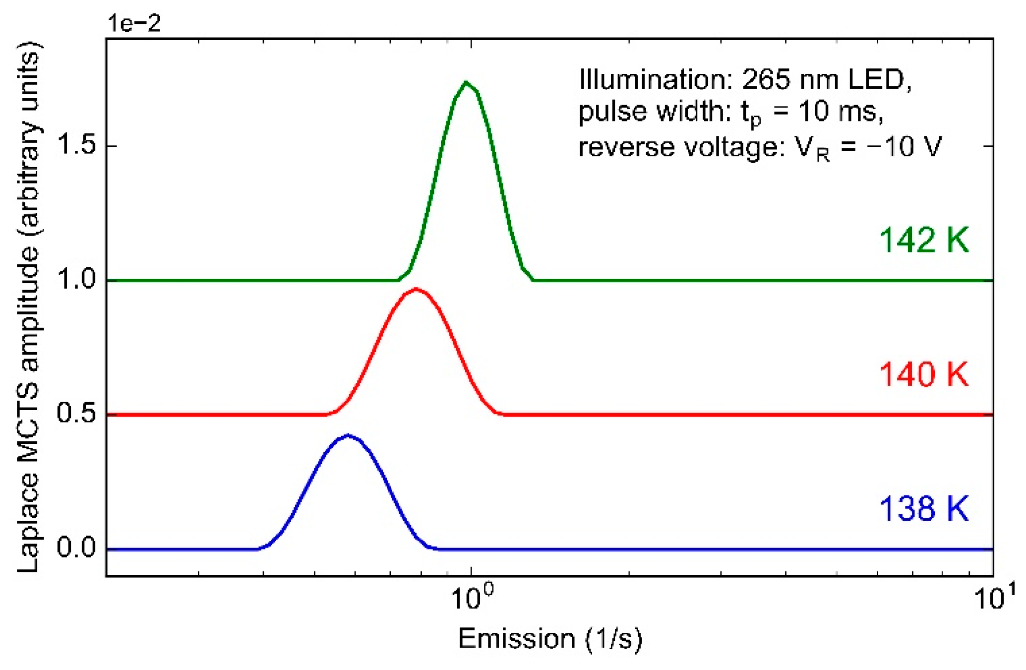
In addition, we analyzed the
Ev + 0.28 eV trap by means of Laplace MCTS measurements, as shown in
Figure 5. A well-defined single emission line was detected.
To the best of our knowledge, the
Ev + 0.28 eV trap resembles the hole trap reported by Beyer at al. [
3]. In their study, a hole trap was observed in the
n-type (Fe-doped) 4H–SiC SBD with an energy level of
Ev + 0.29 eV. They assigned this trap to boron-related defects since Secondary ion mass spectrometry (SIMS) measurements revealed the presence of boron ([B] = 8.9 × 10
14 cm
3). The incorporation of boron in
n-type (Fe-doped) 4H–SiC material was explained by the presence of boron in the graphite susceptor used for the chemical vapor deposition (CVD) growth process.
We estimated the concentration of
Ev + 0.28 eV defects from the MCTS measurements (
Figure 3) and obtained a value of about 6 × 10
12 cm
−3. This result should be taken with caution since we detected not only minority carrier traps. This issue is discussed later in the text.
Based on the comparison with the available literature data and a similar CVD growth process [
3], we assigned the
Ev + 0.28 eV trap to boron-related defects.
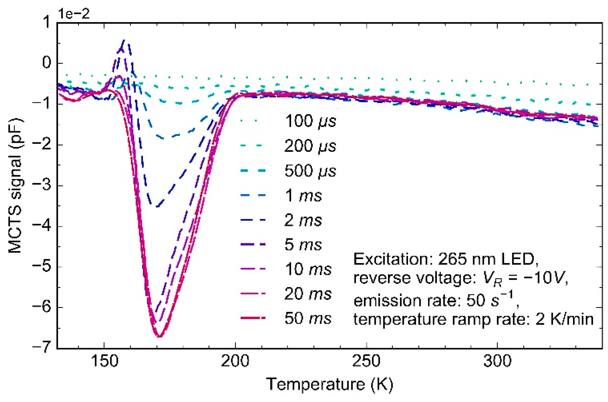
To obtain additional information, we performed a series of MCTS/Laplace-MCTS measurements by varying the optical pulse widths (from 100 µs up to 50 ms).
Figure 6 shows selected MCTS spectra for different optical excitation pulse widths. Although the MCTS peaks for the
Ev + 0.28 eV trap are broad (
Figure 6) for the short pulses (1–2 ms) and exhibit a shape similar to double peaks (two closely spaced peaks), the Laplace-MCTS measurements showed a single emission line (as shown in
Figure 6) and did not reveal any new information regarding the
Ev + 0.28 eV trap. In addition, a small positive peak in the MCTS spectrum with its peak maximum around 160 K was detected. We were not able to precisely estimate the activation energy of this trap (due to the inconsistent behavior either through the series of Laplace-MCTS measurements at different temperatures or for different optical excitation pulse widths) and it remains unclear is it a majority carrier trap or an artefact of the measurements.
The positive peak could be caused by the electron emission from the deep level to the conduction band. The capture of electrons at majority carrier traps during the light pulse could occur if the electron current inside the space charge region is not negligible compared to the hole current or if photoionization effects are not negligible.
Majority carrier traps could also be detected by MCTS, as usually occurs when optical excitation goes from the front contact of an SBD. In that case, optical excitation generates both majority and minority carriers in the depletion region. Depending on the capture cross-section, i.e., if the minority carrier cross-section of the present trap is greater than the majority carrier cross-section, the trap will be occupied by minority carriers and will be observed in the MCTS spectrum [
6].
Basically, Laplace-MCTS measurements can enable us to estimate the temperature-dependent hole capture cross-section. In their pioneering work, Hamilton et al. [
7] described the method for the calculation of hole capture cross-section and indicated the main parameters and approximations that are prerequisites for the correct calculation in the simple MCC model.
We tested this method in order to estimate the temperature-dependent hole capture cross-section. MCTS measurements (
Figure 6) showed that the measured transients are not well-defined exponential transients. Consequently, the simple MCC model could not be used without any doubt. One explanations for this is the fact that we used front-side illumination. In this case, both majority and minority carriers are present in the depletion region and they both play a part in the capture kinetics [
6]. The presence of a small but still detectable positive peak in the MCTS spectra (
Figure 6) supports this statement.
