Article

Spatial Beam Filtering with Autocloned Photonic Crystals

Department of Electro-Optical Engineering, National Taipei University of Technology, No. 1, Sec. 3, Chung-Hsiao E. Rd, Taipei 10608, Taiwan
*
Author to whom correspondence should be addressed.
Crystals 2019, 9(11), 585; https://doi.org/10.3390/cryst9110585
Submission received: 18 October 2019 / Revised: 5 November 2019 / Accepted: 6 November 2019 / Published: 8 November 2019
(This article belongs to the Special Issue Sonic and Photonic Crystals)

Abstract

:
We have been numerically demonstrated the mechanism of spatial beam filtering with autocloned photonic crystals. The spatial filtering through different configurations of the multilayered structures based on a harmonically modulated substrate profile is considered. The paper demonstrates a series of parameter studies to look for the best spatial beam filtering performance. The optimization results show that a beam spectral width of 39.2° can be reduced to that of 5.92°, leading to high potential applications for integrated optical microsystems.

1. Introduction

Angular/spatial filtering devices based on photonic crystals (PhCs) [1,2] provide diffraction of the angular components of an incident beam. The effect of a PhCs-based spatial/angular filtering device that works on a spatial frequency spectrum relies on an angular band-gap [3,4,5,6,7]. For spatial filtering, a range of angular components of a beam can be removed due to the angular band-gaps, that is, the waves can be reflected in a backward direction [3,4,5] or deflected at large angles in a forward one [6,7].
Furthermore, double-periodic photonic structures enable manipulation of the zero diffraction order of a transmitted beam [8]. For example, some angular components of an incident light source diffract from the zero diffraction order to the other orders at resonance conditions. On the other hand, some angular components, out of resonance, directly propagate through the PhCs. In this way, low-angle-pass or high-angle-pass filtering devices are achievable through a proper interplay among the grating characteristics.
In particular, the PhCs filtering has been already implemented for intracavity angular filtering in an integrated platform such as microchip lasers [9]. Such a PhCs-based confocal filtering device presents an alternative method for replacing conventional filtering devices [10], but has a critical disadvantage that is the presence of an optical axis [11]. Therefore, the transmitted axisymmetric concentric ring structures result in the limitation of angular filter merely for on-axis incident light.
It is noted that there have been other approaches to spatial filtering such as passive [12] or light-induced [13] Bragg gratings and pulse-induced population density gratings [14]. However, these alternative methods require not only more sophisticated schemes but additional optical components, leading to limited applications in the compact micro-systems. Therefore, more compact PhCs-based angular filters are desirable solutions for the use in the microlasers, e.g., autocloned PhCs, which preserves the initial modulation during the deposition of multilayers [15]. For example, a multilayered photonic microstructure based on a sinusoidal or braze profile was demonstrated experimentally as one of the most compact PhCs-based angular filters [16]. However, this proposed filter presents the weak filtering performance, so further investigation is required for practical use. For example, a compact filter with a transverse invariance performs both the narrow angular bandwidth and the high efficiency. The filtering for the application of such a compact filter toward a Gaussian beam has not been well studied in the prior study [16]. Although the fabrication of the autocloned PhCs has been demonstrated experimentally [17,18], it is still unavoidable that the variation of the amplitude (Amp) of the harmonic modulation of the autoclaved PhCs increases with the number of layers [19]. Further studies for feasible parameters in fabrication such as less number of layers are a concern.
In this paper, we provide a numerical study of an angular/spatial filtering based on multilayered PhCs gratings with a harmonically modulated substrate profile. The multilayered gratings are all-dielectric and periodic, where the variation of the periods or wavelength results in a low- or high-angle-pass filter. A spectral width (SW), defined as the full spectral width at half maximum (FWHM), is calculated by using the finite-difference time-domain (FDTD) method [20]. To enhance the spatial filtering, we focus on narrowing filtering angular distributions by the design of the low-angle-pass filter and the results are compared with the study in [16].

2. Numerical Far-Field Simulations for Autocloned PhCs

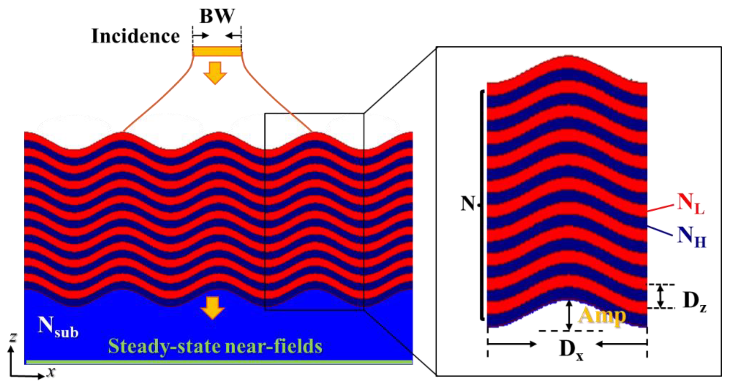
The configuration of the proposed multilayered PhCs grating for spatial filtering is schematically shown in Figure 1. The multilayers consisting of alternating high-refractive-index (NH) and low-refractive-index (NL) layers with the number of layers (N) on top of a grating substrate (Nsub) that results in a sinusoidal profile with a peak-to-peak Amp. Such a multilayered grating with a sinusoidal profile provides a transversal and a longitudinal modulations of the period (Dx) and an alternating thicknesses (Dz) of the multilayers. The thicknesses of the high- and low-refractive-index layers are equal to Dz/2. The wavelength of the incident light is equal to λ = 582 nm and a transverse electric (TE) polarization is considered. A more detailed calculation procedure is further described in the following section, Method.
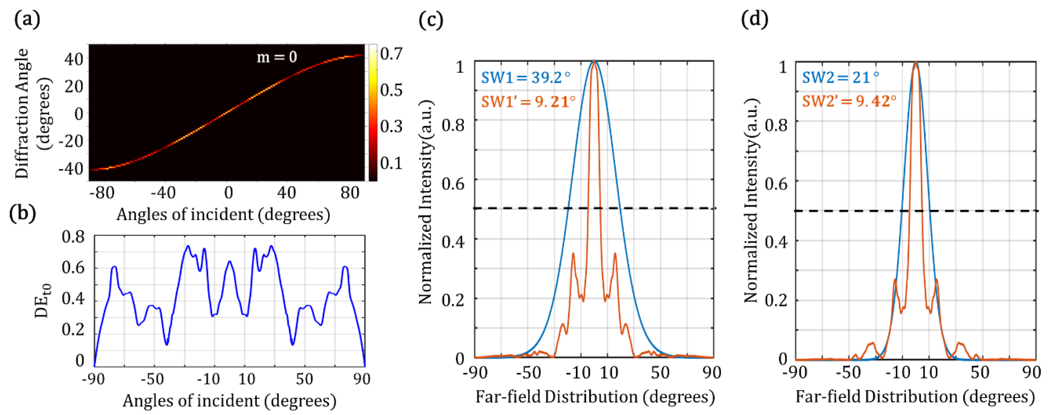
We first analyze diffraction patterns of the periodic multilayered structure by using a rigorous coupled-wave analysis (RCWA) method [21] and its 0th-order transmission is as plotted in Figure 2a. The parameters of the studied structure are identical as those in [16]: N = 33 layers, Dx = 1.67 μm, Dz = 0.24 μm, NSub = 1.5, NH = 1.42, and NL = 1.3. Since the parameter of Amp was not mentioned in [16], we found the narrowest SW by scanning Amp up to 0.5 μm. The narrowest SW of 9.21° is obtained for Amp = 0.27 μm. Furthermore, the angular dependence of the 0th-order diffraction efficiency (DEt0) (Appendix A Method) presents a low-pass filtering design where the angular components at around 10° are removed or coupled out to the others, as shown in Figure 2b. Thus, the far-field distribution of a Gaussian beam, regarded as different plane-wave components at different angles of incidence, can be narrowed down. Figure 2c,d show that the filtered far-field distributions for two incident beams with different beam widths (BW1= 1 λ and BW2 = 2 λ). Their filtered SWs, SW1’ (9.21°) and SW2’ (9.42°), are narrower than SW1 (39.2°) and SW2 (20.99°), respectively.

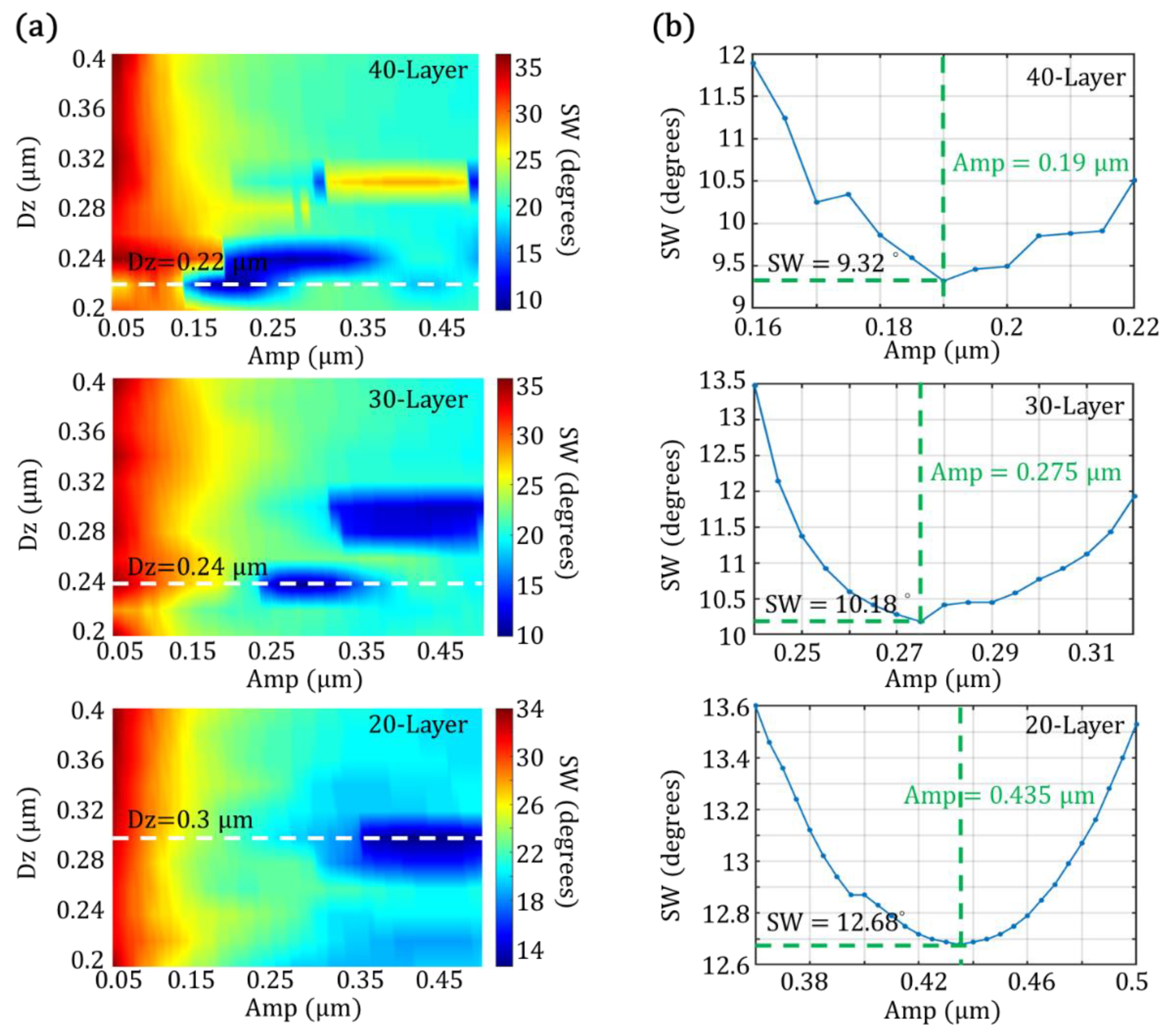
3. Minimum SWs for Different Configurations of Autocloned PhCs

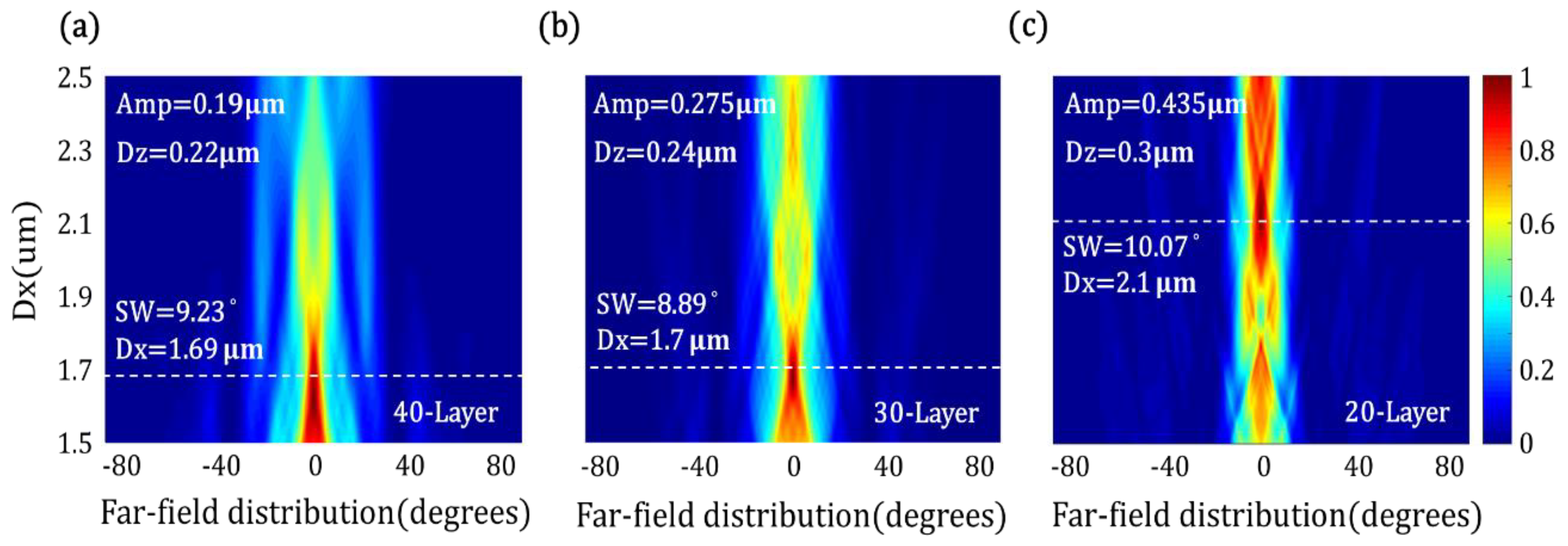
In this section, a series of numerical calculations is executed for the best filtering effect. We focus on scanning structural parameters such as Amp and Dz for obtaining a narrow FWHM of SW. First, three configurations of the wavy structures are considered with different layer numbers (N = 40, 30, and 20). Three related maps of their SWs are calculated by scanning two parameters Amp from 0.005 to 0.5 μm and Dz from 0.2 to 0.4 μm, as shown in Figure 3a. It is noted that their transversal periods are identical, referred to [15].
The smallest SWs for the 40-, 30-, and 20-layer configurations are found at the longitudinal periods Dz of 0.22, 0.24, and 0.3 μm, respectively. The corresponding variances of the SWs at the specific Dz, highlighted by white dashed lines in Figure 3a, are shown in Figure 3b. The optimal Amps of these three harmonic structures with N = 40, 30, and 20 are 0.19, 0.275, and 0.435 μm, respectively. As a result, in the three configurations with the different layer numbers, the 40-layer structure presents the smallest SW of 9.32° where BW of 1 λ is considered.
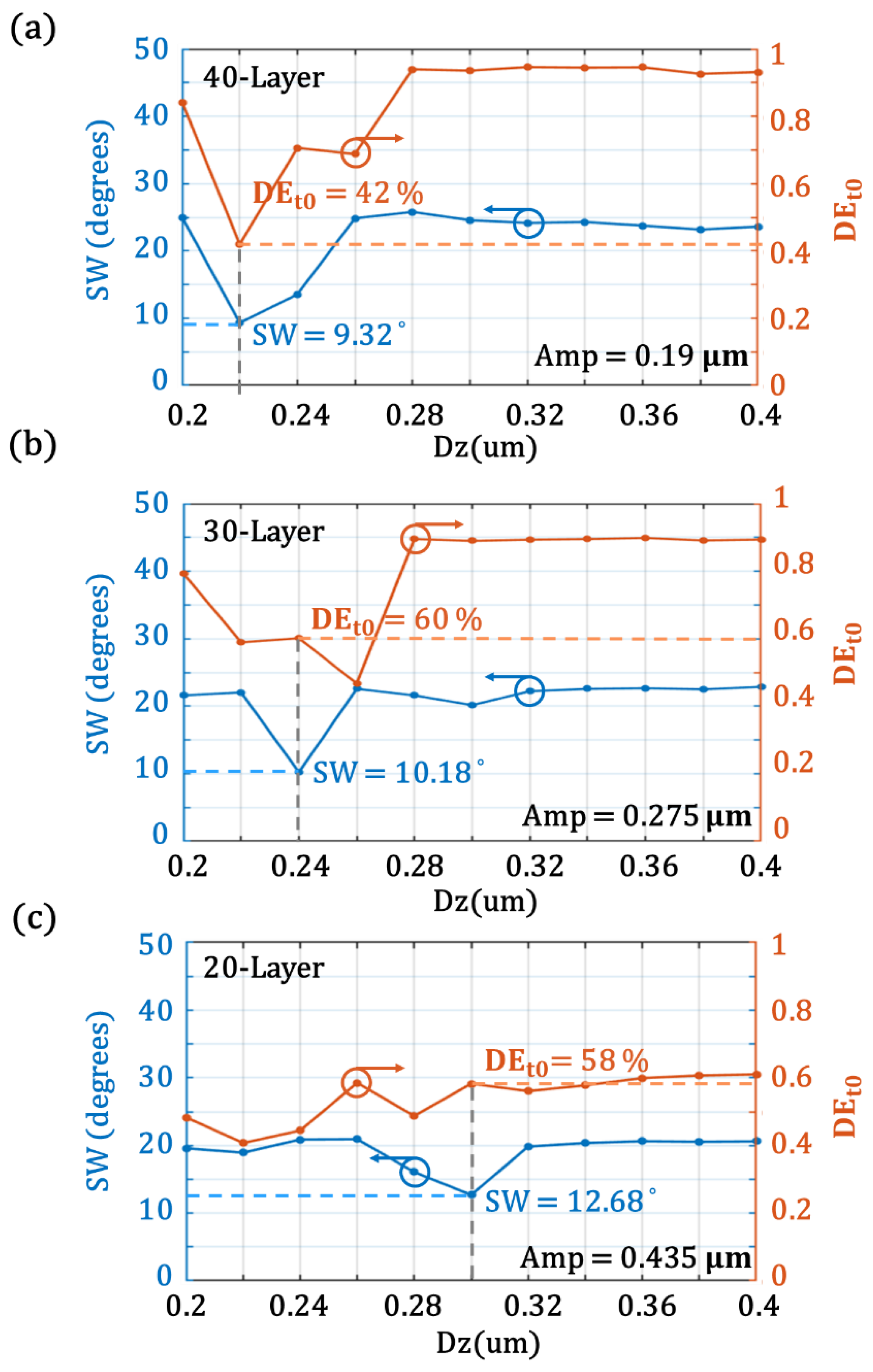
Furthermore, the diffraction efficiency for the center of the filtered beam is also considered as depicted in Figure 4. The variations of the SW and DEt0 with respect to Dz are studied for the three different configurations of the wavy structures. The SWs of 9.32°, 10.18°, and 12.68° and DEt0 values of 42%, 60%, and 58% are achievable for the 40-, 30-, and 20-layer structures, respectively. Although the narrowest SW of 9.32° of a filtering beam is achievable by the configuration with 40 layers, it brings in the lowest diffraction efficiency.
For all the above simulations, the transversal period Dx of 1.67 μm is considered for the low-pass filtering design. As generally known, the transversal period of PhCs plays an important role in diffraction patterns. As the transversal period Dx is changed, the far-field distribution changes dramatically, leading to the low- and high-pass filtering effects. Hence, Figure 5 shows the variation of far-field distributions by varying Dx for three configurations with 40-, 30-, and 20-layer structures. The best low-angle-pass filtering performance (SW = 8.89° and DEt0 = 60%) is found at the 30-layer structure with Amp = 0.275 μm, Dz = 0.24 μm, and Dx = 1.7 μm.
A more optimal parameter Dx of 1.7 μm is found after scanning the far-field distribution with respect to Dz, as shown in Figure 4. Even though the longitudinal period Dx of 1.67 μm is considered for the previously studied structure, it has shown that the procedure of the search of optimal parameters such as Amp, layers, and Dz for the low-pass angular filtering is beneficial. For example, as shown in Figure 3 and Figure 4, we obtain SWs of 12.68° and 9.32° and DEt0 values of 58% and 42% for the two configurations with 20 layers and 40 layers, respectively. Although the 40-layer structure presents stronger spatially filtering, it requires more layers to achieve the narrower SW; however, the DEt0 is lower.
Furthermore, the number of layers is also a concern for the fabrication of a wavy-like multilayered structure because the experimental modulation of the wavy structure may be reduced with the increased number of layers [19]. Even if the fabrication of the 20-layer structure may be controllable, a weaker filtering effect is obtained. Obviously, the fabricating feasibility concerning the number of layers should be also considered at the stage in the design process. Therefore, a series of the analysis of structural parameters is helpful to define the optimization range and consider fabrication feasibility.
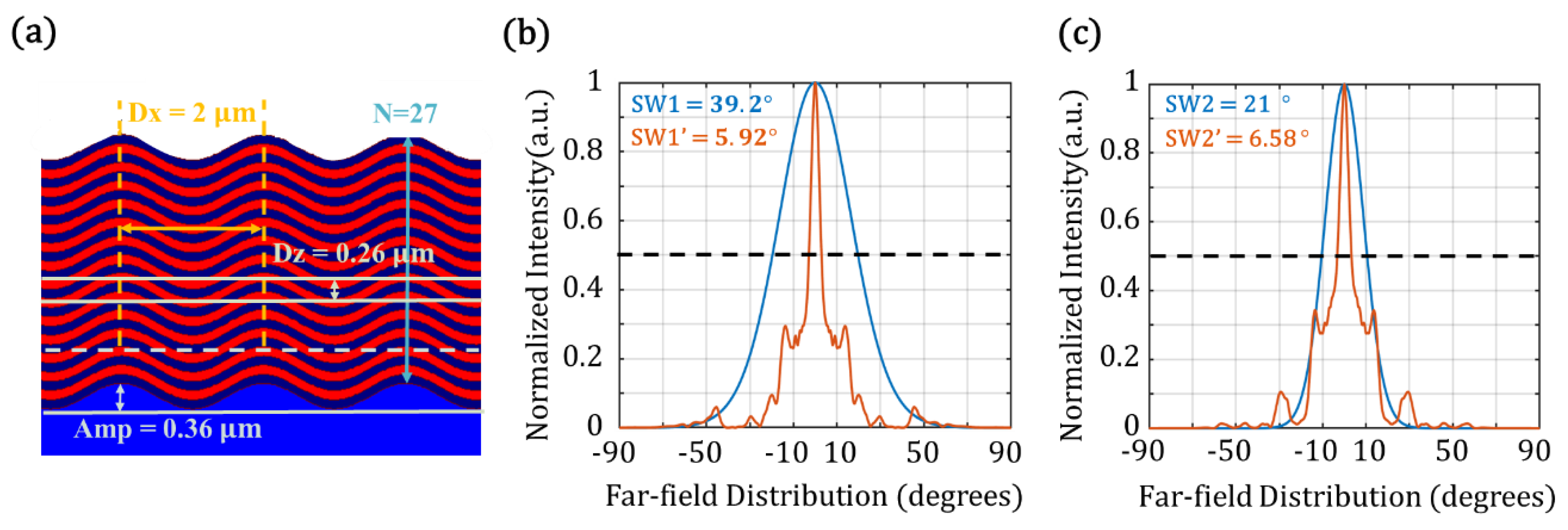
In our work, the optimization of this wavy structure by using the simplex method has been demonstrated, as shown in Figure 6. All parameters of the multilayered structure are optimized simultaneously and the target of the optimization is to realize a low-pass filter design that achieves the narrowest SW for a Gaussian beam. To ensure fabrication feasibility, the optimizing range of the number of the layer should not be more than 40 layers. The optimizing ranges of Amp and the longitudinal period Dz should be less than 0.5 μm and 0.4 μm, respectively, as referred to the previous study. As a result, the final optimal parameters of the structure are obtained as follows: N = 27, Amp = 0.36 μm, Dz = 0.26 μm, and Dx = 2 μm. The far-field distributions in Figure 6b,c show the narrowest SW1’ = 5.92° and SW2’ = 6.58° for two Gaussian beams with BW1 = λ and BW2 = 2λ, respectively. The DEt0 of the optimal result is 64%. The narrower SW and the higher diffraction efficiency are achieved by the optimized structure with the less number of layer, compared with that of the previous study. Therefore, the optimizing results not only present the best spatial filtering to narrow the SW, but also demonstrate the use of the structures with fewer layers is a more feasible approach to a manufacturing process.

4. Conclusions

This paper has demonstrated the PhCs filtering effect for a light beam. The autocloned PhCs present transversal and longitudinal periods, the key element to modulate spatial spectra. The paper has studied different configurations of the multilayered structures based on the harmonic modulation. The narrowest SW of 8.89° and the diffraction efficiency of 60% are obtained for a 30-layer structure after a series of the scanning procedure in the structural parameters.
Considering feasible fabrication, the optimization has been further studied for practical use by using the simplex method. The number of layers N for our optimal structure is reduced to 27 and a stringer spatial filtering performance provides an SW of 5.92° and the diffraction efficiency of 0th transmission is 64%. For an autocloned PhC with several layers, another approach, such as an autocloned blazed modulation, could be more applicable for fabrication, although the fabrication of a tilted blazed profile is not as simple as that of the sinusoidal modulation.

Author Contributions

Conceptualization, Y.-C.C.; methodology, software and validation, Y.-C.C., Y.-C.L. and P.-Y.W.; investigation, writing—original draft preparation, writing—review and writing—editing, Y.-C.C. and P.-Y.W.; visualization, Y.-C.C., P.-Y.W. and Y.-C.L.; supervision, Y.-C.C.; funding acquisition, Y.-C.C.

Funding

This work was financially supported by the Young Scholar Fellowship Program by the Ministry of Science and Technology (MOST) in Taiwan, under grant number MOST108-2636-M-027-001.

Acknowledgments

The authors would like to thank the Headquarters of University Advancement at National Cheng Kung University (NCKU) for the funding support of the Higher Education Sprout Project of Ministry of Education (MOE).

Conflicts of Interest

The authors declare no conflict of interest. The funders had no role in the design of the study; in the collection, analyses, or interpretation of data; in the writing of the manuscript, or in the decision to publish the results.

Appendix A. Method

The diffraction efficiency of zero-order transmission is calculated by using the RCWA method, which solves full vectorial versions of Maxwell’s equations. It covers a wide range of scattering problems on the wavy structures with horizontally periodic boundary conditions and vertically perfectly matched layer (PML) boundary. The incident and transmitted fields are defined at the simulation domain along the z-direction. A plane wave incidence is used in the RCWA simulation.
The far-field distribution is obtained by using two methods. First, the FDTD method provides steady-state near-field distributions at an output plane while an incident Gaussian beam with a BW considered. Second, we use the discrete Fourier transform (DFT) to convert the steady-state near-field distribution to the far-field distribution. The SW is defined as the FWHM of the far-field distribution. The Gaussian beam is launched at the position of 1 μm above the wavy structure. The horizontal simulation domain is equal to 50 periods of the proposed wavy structure and the vertical boundary condition is the PML.

References

  1. Yablonovitch, E. Inhibited Spontaneous Emission in Solid-State Physics and Electronics. Phys. Rev. Lett. 1987, 58, 2059–2062. [Google Scholar] [CrossRef] [PubMed] [Green Version]
  2. Sajeev, J. Strong localization of photons in certain disordered dielectric superlattices. Phys. Rev. Lett. 1987, 58, 2468–2489. [Google Scholar]
  3. Luo, Z.; Tang, Z.; Xiang, Y.; Luo, H.; Wen, S. Polarization-independent low-pass spatial filters based on one-dimensional photonic crystals containing negative-index materials. Appl. Phys. B 2009, 94, 641–646. [Google Scholar] [CrossRef]
  4. Colak, E.; Cakmak, A.O.; Serebryannikov, A.E.; Ozbay, E. Spatial filtering using dielectric photonic crystals at beam-type excitation. J. Appl. Phys. 2010, 108, 113106. [Google Scholar] [CrossRef]
  5. Hamam, R.E.; Celanovic, I.; Soljačić, M. Angular photonic band gap. Phys. Rev. A 2011, 83, 035806. [Google Scholar] [CrossRef]
  6. Maigyte, L.; Gertus, T.; Peckus, M.; Trull, J.; Cojocaru, C.; Sirutkaitis, V.; Staliunas, K. Signatures of light-beam spatial filtering in a three-dimensional photonic crystal. Phys. Rev. A 2010, 82, 043819. [Google Scholar] [CrossRef]
  7. Maigyte, L.; Staliunas, K. Spatial filtering with photonic crystals. Appl. Phys. Rev. 2010, 2, 011102. [Google Scholar] [CrossRef]
  8. Purlys, V.; Maigyte, L.; Gailevicius, D.; Peckus, M.; Malinauskas, M.; Staliunas, K. Spatial filtering by chirped photonic crystals. Phys. Rev. A 2013, 87, 033805. [Google Scholar] [CrossRef]
  9. Gailevicius, D.; Koliadenko, V.; Purlys, V.; Peckus, M.; Taranenko, V.; Staliunas, K. Photonic Crystal Microchip Laser. Sci Rep. 2016, 6, 34173. [Google Scholar] [CrossRef] [PubMed]
  10. Chen, G.; Leger, J.R.; Gopinath, A. Angular filtering of spatial modes in a vertical-cavity surface-emitting laser by a Fabry–Perot étalon. Appl. Phys. Lett. 1999, 74, 1069–1071. [Google Scholar] [CrossRef]
  11. Koch, B.J.; Leger, J.R.; Gopinath, A.; Wang, Z.; Morgan, R.A. Single-mode vertical cavity surface emitting laser by graded-index lens spatial filtering. Appl. Phys. Lett. 1997, 70, 2359–2361. [Google Scholar] [CrossRef]
  12. Svyakhovskiy, S.E.; Skorynin, A.A.; Bushuev, V.A.; Chekalin, S.V.; Kompanets, V.O.; Maydykovskiy, A.I.; Murzina, T.V.; Mantsyzov, B.I. Experimental demonstration of selective compression of femtosecond pulses in the Laue scheme of the dynamical Bragg diffraction in 1D photonic crystals. Opt. Express. 2014, 22, 31002–31007. [Google Scholar] [CrossRef] [PubMed] [Green Version]
  13. Brown, A.W.; Xiao, M. All-optical switching and routing based on an electromagnetically induced absorption grating. Opt. Lett. 2005, 30, 699–701. [Google Scholar] [CrossRef] [PubMed] [Green Version]
  14. Arkhipov, R.M.; Pakhomov, A.V.; Arkhipov, M.V.; Babushkin, I.; Demircan, A.; Morgner, U.U.; Rosanov, N.N. Population density gratings induced by few-cycle optical pulses in a resonant medium. Sci. Rep. 2017, 7, 12467. [Google Scholar] [CrossRef] [PubMed]
  15. Kawakami, S. Fabrication of submicrometre 3D periodic structures composed of Si/SiO/sub 2/. Electron. Lett. 1997, 33, 1260–1261. [Google Scholar] [CrossRef]
  16. Grineviciute, L.; Babayigit, C.; Gailevičius, D.; Bor, E.; Turduev, M.; Purlys, V.; Tolenis, T.; Kurt, H.; Staliunas, K. Angular filtering by Bragg photonic microstructures fabricated by physical vapour deposition. Appl. Surf. Sci. 2019, 481, 353–359. [Google Scholar] [CrossRef]
  17. Ohtera, Y.; Kawashima, T.; Sakai, Y.; Sato, T.; Yokohama, I.; Ozawa, A.; Kawakami, S. Photonic crystal waveguides utilizing a modulated lattice structure. Opt. Lett. 2002, 27, 2158–2160. [Google Scholar] [CrossRef] [PubMed]
  18. Notomi, M.; Shinya, A.; Kuramochi, E.; Yokohama, I.; Tamamura, T.; Takahashi, J.; Takahashi, C.; Kawashima, T.; Kawakami, S. Si-Based Composite-Dimensional Photonic Crystals towards Si Photonics, Technical Digest. In Proceedings of the CLEO/Pacific Rim 2001 4th Pacific Rim Conference on Lasers and Electro-Optics, Chiba, Japan, 15–19 July 2001. [Google Scholar]
  19. Huang, C.Y.; Ku, H.M.; Chao, S. Surface profile control of the autocloned photonic crystal by ion-beam-sputter deposition with radio-frequency-bias etching. Appl. Opt. 2009, 48, 69–73. [Google Scholar] [CrossRef] [PubMed]
  20. Taflove, A. Computational Electrodynamics: The Finite-Difference Time-Domain Method; Artech House: Norwood, MA, USA, 1995; pp. 93–105. [Google Scholar]
  21. Moharam, M.G.; Grann, E.B.; Pommet, D.A.; Gaylord, T.K. Formulation for stable and efficient implementation of the rigorous coupled-wave analysis of binary gratings. J. Opt. Soc. Am. A 1995, 12, 1068–1076. [Google Scholar] [CrossRef]
Figure 1. Illustration of the proposed autocloning photonic crystals (PhCs) with a harmonic modulation. The inset shows the parameters of the wavy structure. Dx and Dz represent the horizontal and longitudinal periods, respectively. N is the number of layers. Low- and high-refractive-index materials are shown in red and blue colors, respectively. The parameter Amp indicates the peak-to-peak value of the multilayer structure, also regarded as the amplitude of the harmonic modulation. The beam width (BW) represents the full spectral width at half maximum (FWHM) of a launched beam. The steady-state near-field plane is defined as the output plane of the simulation domain.
Crystals 09 00585 g001
Figure 2. Numerical far-field simulation of autocloning-mode-based PhCs: (a) the diffraction map of 0th order versus angles of incidence; (b) diffraction efficiency of 0th-order transmission (DEt0) with respect to angles of incidence; far-field distributions for two different incident Gaussian beam widths: (c) BW1 = λ; (d) BW2 = 2λ. The parameters of the structure in (a) and (b) are as following: N = 33 layers, Amp = 0.27 μm, Dz = 0.24 μm, and Dx = 1.67 μm. These two spectral width SW1 and SW2 mean the FWHM of the spectral width of the Gaussian beam for BW1 = λ and BW2 = 2λ, respectively. SW1 and SW1’ in (c) represent the normalized far-field distributions of the Gaussian beam passing without PhCs in blue and with the PhCs in red for BW1 = λ. SW2 and SW2’ in (d) represent the normalized far-field distributions of the Gaussian beam passing without PhCs in blue and with the PhCs in red for BW2 = 2λ.
Crystals 09 00585 g002
Figure 3. (a) The SWs of autocloning-mode-based PhCs structures with different amplitudes of harmonic modulation and longitudinal periods Dz for different layer structures. The smallest SW can be obtained at Dz indicated by the dashed white lines. (b) Variation of the SW as a function of Amp at Dz indicated by the dashed white lines in (a).
Crystals 09 00585 g003
Figure 4. The smallest SWs and the 0th-order diffraction efficiency (DEt0) varied with the longitudinal period Dz for three autocloning-mode-based PhCs with N = 40 layers (a), 30 layers (b), and 20 layers (c). The minimum of the SW of 9.32° can be obtained for the 40-layer structure at Dz = 0.22 μm and Amp = 0.19 μm. The minimum of the SW of 10.18° can be obtained for the 30-layer structure at Dz = 0.24 μm and Amp = 0.275 μm. The minimum of the SW of 12.68° can be obtained for the 20-layer structure at Dz = 0.3 μm and Amp = 0.435 μm. The DEt0 values of the 40-, 30-, and 20-layered structure are 42%, 60%, and 58%, respectively. The transversal period Dx is constant, i.e., 1.67 μm.
Crystals 09 00585 g004
Figure 5. 2-D maps of normalized far-field distributions with respect to the angle of incidence and transversal period Dx for the multilayered structures with 40 layers (a), 30 layers (b), and 20 layers (c). In the 40-layer structure, the minimum FWHM is 9.23° at Dx = 1.69 μm with the DEt0 of 39%. In the 30-layer structure, the minimum FWHM is 8.89° at Dx = 1.7 μm with the DEt0 of 60%. In the 20-layer structure, the minimum FWHM is 10.07° at Dx = 2.1 μm with the DEt0 of 49%.
Crystals 09 00585 g005
Figure 6. The optimization results of the wavy structure by using the simplex method. (a) The illustration of the optimal structures with parameters: N = 27, Amp = 0.36 μm, Dz = 0.26 μm, and Dx = 2 μm. Far-field distributions for two different incident Gaussian beam widths BW1 = λ (b) and BW2 = 2λ (c), where λ is the operating wavelength. The narrowest FWHM of a Gaussian beam with BW = λ is 5.92°.
Crystals 09 00585 g006

