1. Introduction
Over the past few decades, the development of display technologies has advanced rapidly, with various display applications, such as televisions, large advertising billboards, and computers, being widely used across numerous fields, thereby driving the progress of modern society [
1]. In recent years, Liquid Crystal Display (LCD) and Organic Light Emitting Diode (OLED) technologies have seen widespread adoption and have gradually come to dominate the display market. Although LCD and OLED technologies are extensively applied in daily life, both still face challenges related to issues such as lifespan, response time, and brightness, which hinder their ability to meet the growing demand for higher-quality displays [
2]. Moreover, with the emergence of new applications in display technology, such as Virtual Reality (VR) and Augmented Reality (AR), these products demand displays that offer higher brightness, compact size, and lower power consumption. Existing display technologies struggle to meet all these requirements simultaneously. As a result, researchers have focused on miniaturizing and arraying Light Emitting Diodes (LEDs) to develop new products that fulfill these specifications, leading to the rise of μLEDs display technology [
3]. Typically, LEDs with dimensions ranging from 1 to 100 μm are defined as μLEDs [
4]. Compared to LCD and OLED technologies, μLED displays have attracted significant attention due to their advantages, such as long lifespan, small size, high brightness, low power consumption, and high stability, positioning them as a promising candidate for the “next-generation display technology” [
5].
By altering the alloy composition of Gallium Nitride (GaN) (e.g., InGaN), the emission wavelength of LEDs can be tuned, covering a broad spectral range from ultraviolet to red light. This versatility makes GaN an ideal choice for display applications. Blue and green LEDs are typically fabricated using GaN materials, while red LEDs are predominantly made from Aluminum Gallium Indium Phosphide (AlGaInP) [
6]. However, AlGaInP-based μLEDs encounter several significant challenges. First, the size-dependent effects in AlGaInP-based μLEDs are pronounced, making them particularly vulnerable to etching damage, which leads to a substantial degradation in performance [
7]. This is primarily attributed to the relatively long carrier diffusion length and high surface recombination velocity, which is approximately 10
5 cm/s. Additionally, the integration of InGaN and AlGaInP, being distinct material systems, introduces further complexity in the design of driving circuits for full-color display applications, as mismatched electrical characteristics between the materials complicate current driving and synchronization [
8]. From a manufacturing perspective, given the maturity of InGaN-based blue and green μLEDs technologies, InGaN-based red μLEDs remain the best option, as they are compatible with existing production lines. Increasing attention is being directed toward the growth and fabrication of InGaN-based red μLEDs as a more viable solution for realizing full-color displays [
9].
However, compared to GaN-based blue and green μLEDs, GaN-based red μLEDs still face significant challenges in terms of efficiency. To address this issue, researchers have explored various approaches to improve the quality of the epitaxial layer during material growth. Key methods include Pulse Atomic Layer Epitaxy (PALE), Epitaxial Lateral Overgrowth (ELOG), and High-Temperature Annealing (HTA) [
10]. The PALE technique effectively suppresses parasitic reactions by repeatedly switching precursor gas valves, although it presents limitations in terms of growth rate enhancement [
11]. ELOG, on the other hand, utilizes patterned substrates to guide grain growth, significantly reducing threading dislocations density (TDD) and improving the epitaxial layer quality [
12], with patterned sapphire substrates (PSS) playing a crucial role. Jacob et al. achieved an external quantum efficiency (EQE) of 6.5% at approximately 600 nm on patterned sapphire substrates, marking one of the highest reported efficiencies for red/orange InGaN LEDs on PSS in scientific literature [
13]. HTA involves high temperature annealing to induce polarity inversion, thereby reducing defects and further enhancing crystal quality [
14]. These techniques are pivotal for improving LED performance, reducing TDD, and optimizing optoelectronic efficiency. In μLED fabrication, a significant challenge arises as device size reduces, leading to a marked decrease in EQE. This size-dependent degradation, known as the “size effect,” is primarily attributed to sidewall damage induced by the top-down etching process, which generates non-radiative recombination centers and crystal defects [
15]. To mitigate these issues, several technological approaches have been proposed. First, wet treatment and passivation treatments, such as the use of HF, KOH, and TMAH for wet treatment, and the application of dielectric passivation layers like SiO
2 and SiN
x, have been shown to effectively reduce sidewall defects, thereby enhancing light extraction efficiency (LEE) and internal quantum efficiency (IQE) [
16]. Wong et al. enhanced the EQE of 20 × 20 µm
2 LEDs from 24% to 33% by combining HF wet treatment with ALD sidewall passivation [
17]. Additionally, they demonstrated that combining KOH wet treatment with ALD sidewall passivation effectively reduced non-radiative recombination [
18]. Second, selective area growth (SAG) technology, a bottom-up approach, offers a promising alternative to traditional inductively coupled plasma (ICP) etching, significantly reducing damage and improving the overall performance of μLEDs [
19]. Furthermore, the combination of nanostructural engineering and polarization engineering, such as the use of InGaN nanorod structures, has proven to be effective in enhancing optoelectronic properties [
20]. By modulating strain and material polarity, this approach improves exciton binding energy and reduces surface defects, thereby enhancing radiative recombination efficiency [
21]. Lastly, to address doping inefficiencies, techniques such as low-temperature electron-beam irradiation, thermal annealing, and modulation doping have been successfully employed to improve p-type doping in GaN-based materials [
22]. The integration of these advanced material growth and fabrication techniques offers a comprehensive solution to enhance the performance of μLEDs, addressing the key challenges associated with their miniaturization and optimization.
In our previous work, we identified and confirmed the beneficial effects of KOH wet treatment on GaN-based red μLEDs [
23]. Building upon these findings, the present study extends this investigation by employing 80 °C KOH wet treatment for durations of 3 and 5 min. GaN-based red μLED arrays with pixel sizes of 5, 10, 15, and 20 µm were successfully fabricated on patterned sapphire substrates, with the largest array containing up to 40,000 emitting pixels and a maximum pixel density of 1336 PPI. The sidewall morphology of the devices was characterized using scanning electron microscopy (SEM), and their optoelectronic performance, including electroluminescence (EL), was analyzed to evaluate the current-voltage curves, light emission characteristics, efficiency, and so on.
2. Materials and Methods
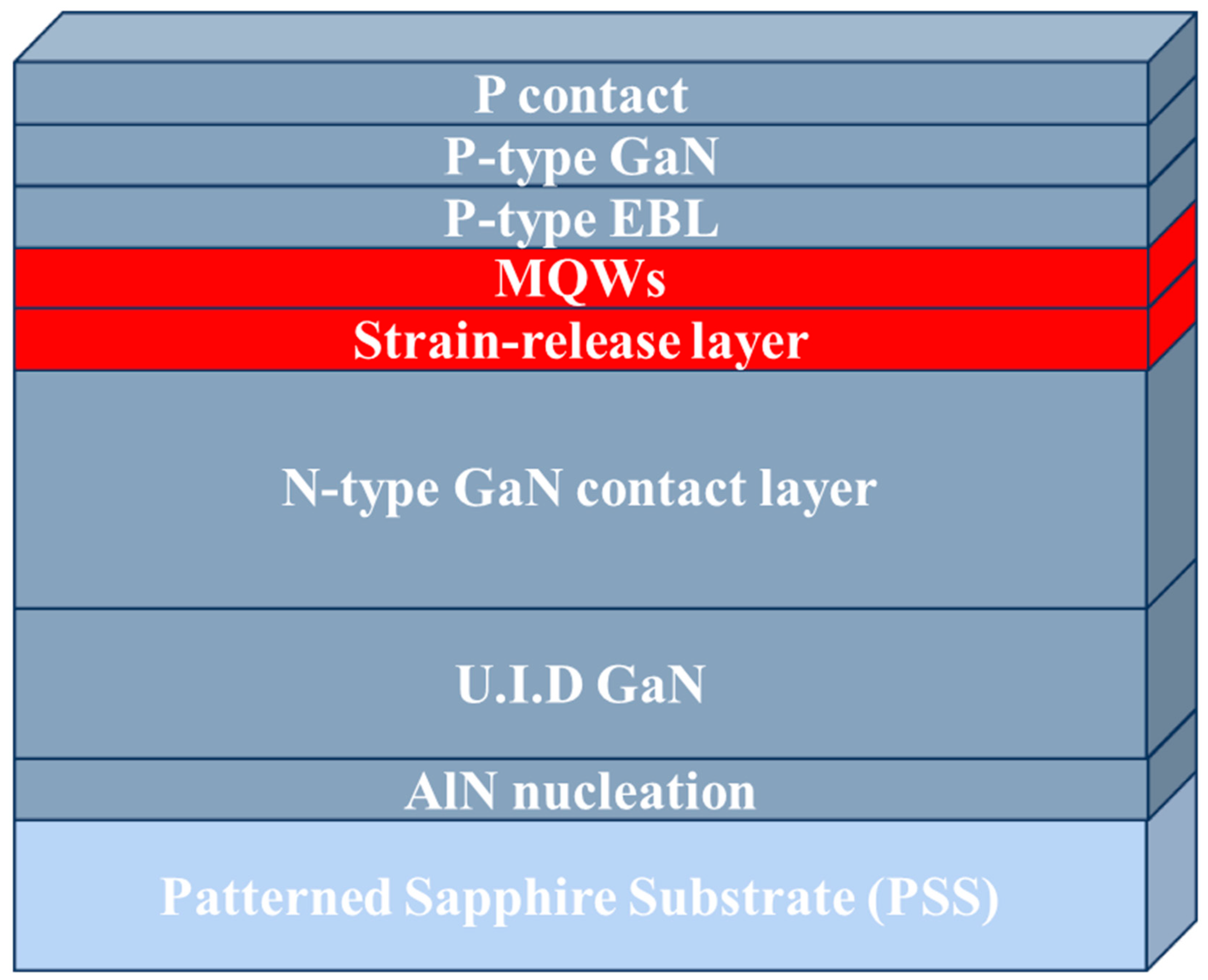
The red μLEDs were epitaxially grown by MOCVD method by Suzhou Hanhua Semiconductors Ltd (Suzhou, China). The epitaxial structure is depicted in
Figure 1. The LEDs were fabricated on a 4-inch patterned sapphire substrate. A 15 nm AlN nucleation layer was first deposited via Physical Vapor Deposition (PVD). The substrate was then introduced into the MOCVD chamber, where a 2.5 µm-thick unintentionally doped GaN buffer layer was grown to achieve surface coalescence. Following this, a 2.5 µm-thick N-type GaN contact layer, doped with Si to a concentration of 5 × 10
18 cm
−3, was grown. Above the N-type contact layer, a 200 nm InGaN-based strain-relief layer was deposited, followed by active region consisting of multiple quantum wells (MQWs). Over the active region, a P-type electron-blocking layer (EBL), a P-type GaN layer, and a P-type contact layer were sequentially grown. All P-type layers were doped with Mg, and the total thickness of the P-type layers was 90 nm. Prior to device fabrication, the LED wafers were annealed ex situ in a furnace under N
2 ambient for Mg dopant activation.
The fabrication process for red μLEDs is depicted in
Figure 2.The epitaxial wafers were initially subjected to both organic and inorganic ultrasonic cleaning, followed by thorough rinsing with deionized water to effectively remove surface particulates and contaminants. After cleaning, an Ni/Au metal layer was deposited onto the wafer surface to form the P-type electrode. The metal layer was then subjected to a lift-off process. Following lift-off, rapid thermal annealing was performed under an O
2 atmosphere at 500 °C for 60 s to establish Ohmic contact and to enhance electrode transparency. Subsequently, a Ti/Ni/Ti reflective layer was deposited via electron beam evaporation. Ti and Ni were selected due to their high reflectivity and superior resistance to wet treatment and over-etching during subsequent patterning processes compared to other metals. After deposition, the sample underwent a lift-off procedure. A layer of SiO
2 (820–830 nm) was grown on the wafer surface by plasma-enhanced chemical vapor deposition (PECVD), serving as a hard mask for subsequent etching. Inductively coupled plasma (ICP) etching was employed to etch the GaN layer down to the n-GaN layer. Following etching, the wafer was immersed in an 80 °C KOH solution for wet treatment, with immersion times of 3 min and 5 min, respectively. The N-type electrode was then fabricated, followed by the deposition of a 2.5 µm thick SiO
2 passivation layer via PECVD for sidewall passivation. Due to the step-like features introduced during the etching process, chemical mechanical polishing (CMP) was employed to achieve a planarized surface. Finally, the SiO
2 layers on both the P-type and N-type electrodes were selectively etched to form via holes, which were subsequently filled with Ti/Al metal to create the μLED array with independent, parallel-connected emitting pixels. The fabrication process for the inverted structure GaN-based red μLED array, as described, yields arrays with 10,000 to 40,000 emitting pixels, pixel densities ranging from 668 PPI to 1336 PPI, and individual pixel sizes ranging from 5 × 5 µm
2 to 20 × 20 µm
2.
3. Results
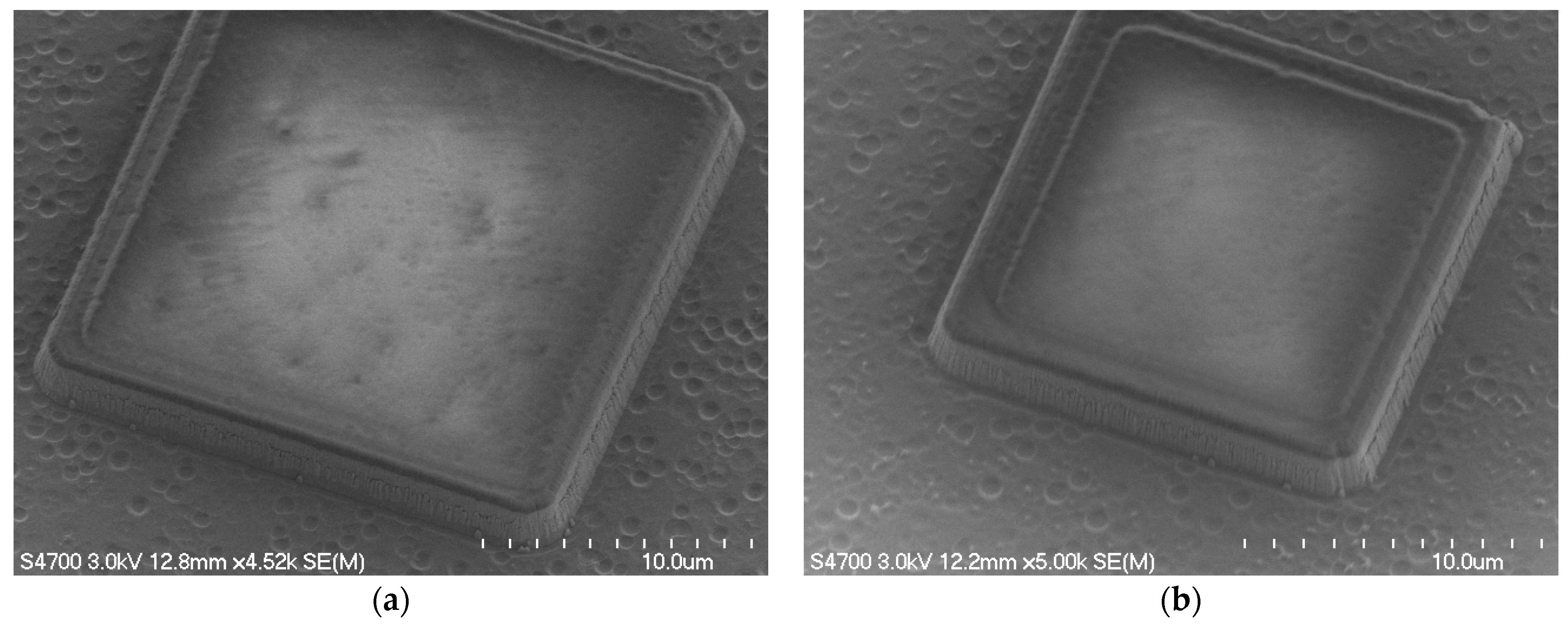
Figure 3 presents SEM images of four pixel sizes after ICP dry etching. The innermost square on the pixel surface represents the metal layer deposited via electron beam evaporation, while the outermost square corresponds to the SiO
2 mask. The overall pixel surface morphology is smooth. However, following the dry etching process, significant sidewall damage is observed across all pixel sizes, with the surface displaying a roughened texture. For smaller pixel sizes, the increased surface-to-volume ratio results in a greater proportion of sidewall damage, which is more pronounced and noticeable.
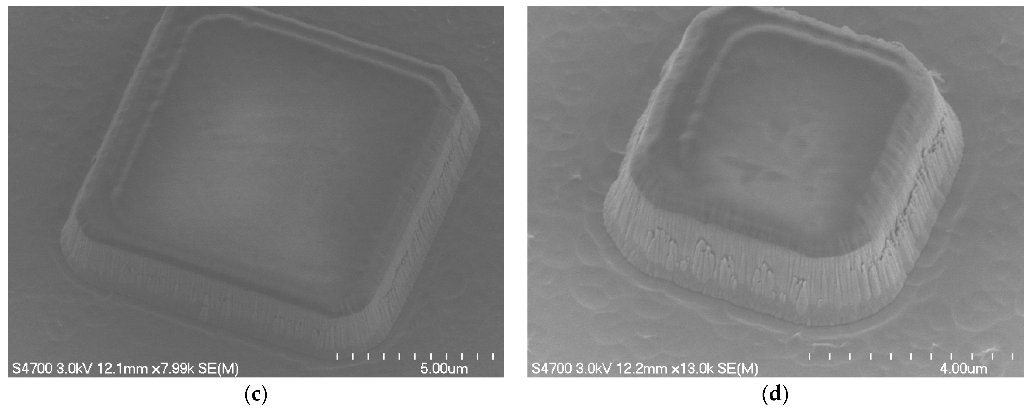
Figure 4 presents the SEM images of pixels with various sizes after being treated in KOH for 3 and 5 min. The left side of the figure shows the SEM images after 3 min of treatment, while the right side shows the images after 5 min. The images, from top to bottom, correspond to pixel sizes of 20, 15, 10, and 5 μm, respectively. It is evident from the images that, regardless of the pixel size, the damage to the sidewalls is significantly reduced during the KOH wet treatment process, with the overall sidewall morphology becoming smoother. This indicates that KOH wet treatment can effectively mitigate the damage to the GaN sidewalls caused by ICP etching in a short period of time and rectify the surface defects on the sidewalls. Moreover, compared to the 3-min treatment, the 5-min KOH wet treatment demonstrates a more pronounced improvement in reducing sidewall damage. However, for extremely small pixel sizes (e.g., 5 μm), after 5 min of KOH wet treatment, the angle between the sidewall and the n-GaN plane increases noticeably, whereas this phenomenon is not observed for 3 min of immersion or for larger pixel sizes. It is proposed that the increased angle between the sidewalls and the base may intensify light scattering and reflection at the pixel edges, thereby adversely impacting the light output power and the uniformity of the emitted beam, resulting in a deterioration of optical performance. Furthermore, excessive KOH treatment may compromise the structural integrity of the pixels, potentially weakening their mechanical strength and introducing additional challenges and risks in subsequent processing steps. Therefore, it can be reasonably inferred from this point that further prolonging the KOH wet treatment time is not advisable. As no signs of over-etching are observed in the SEM images for any of the pixel sizes, we believe that 3-min and 5-min KOH wet treatments are appropriate conditions. Treatment processes effectively improve the sidewall morphology, alleviate dislocations, and mitigate defects of the μLEDs while minimally affecting the overall morphology of the GaN layer.
Table 1 provides a summary of the surface morphology changes and treatment effects described in the preceding text.
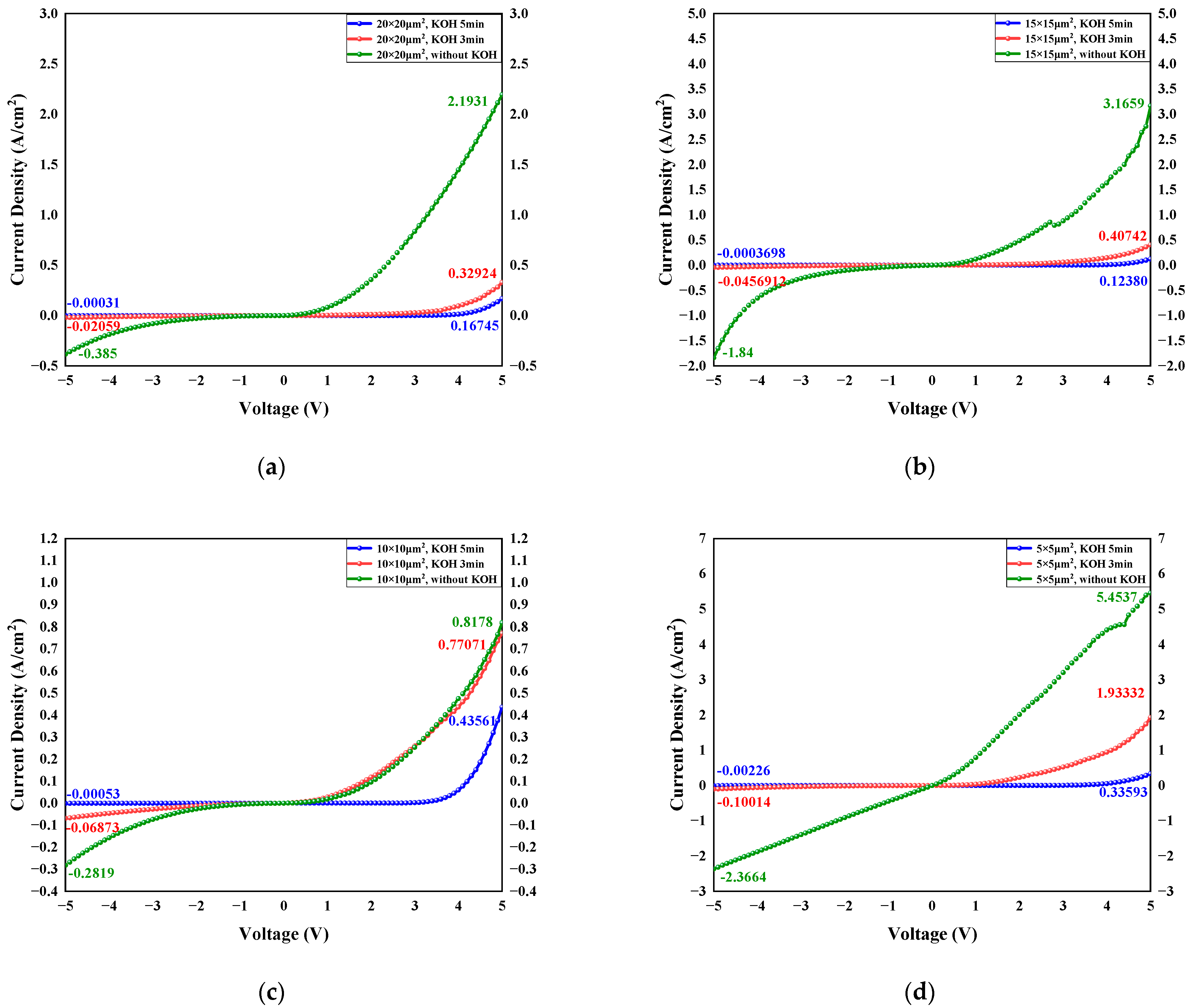
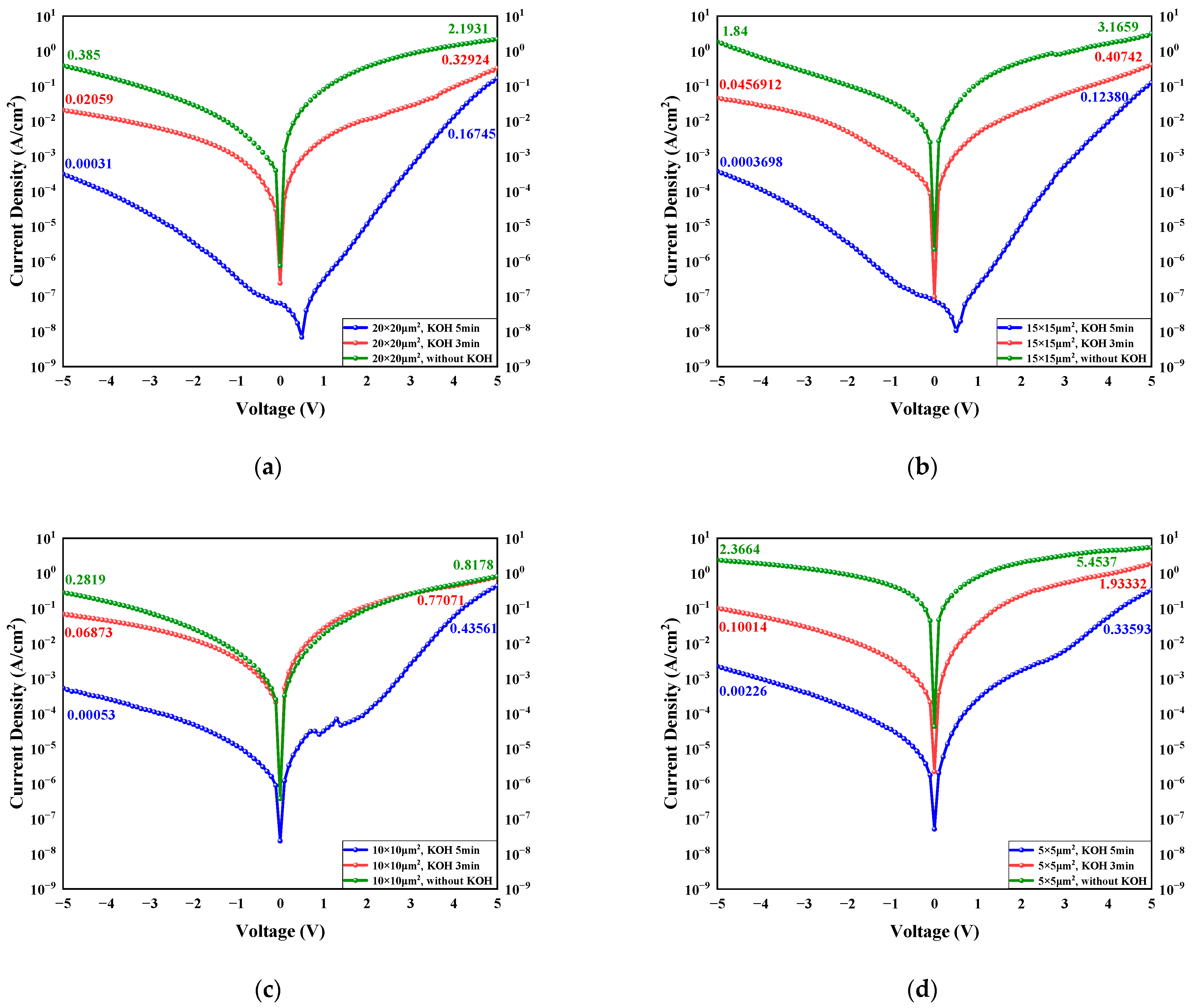
Figure 5 and
Figure A1 present the current-voltage (I-V) curves of the μLED arrays, with the voltage sweep ranging from −5V to 5V, measured with a probe station. The blue curve corresponds to the sample treated with KOH for 5 min, while the red one and green one represents the samples treated for 3 min and without treatment, respectively. All I-V curves exhibit typical PN junction behavior. However, the sample untreated with KOH exhibited no light emission, whereas the samples subjected to KOH wet treatment demonstrated the capability to emit red light. From the figures, it is evident that at a reverse bias of −5V, the leakage current of the arrays untreated with KOH exceeds that of the KOH-treated arrays by at least one order of magnitude. Notably, for the 5 µm pixel arrays, the leakage current density reaches its maximum value of 2.3664 A/cm
2. Since the untreated arrays do not exhibit light emission, only the arrays that are capable of normal light emission—those subjected to KOH wet treatment—are included in the subsequent electroluminescence analysis.
In the forward bias region, the sample treated for 3 min demonstrates a lower threshold voltage, typically 1-2V lower than that of the 5-min treatment, resulting in a higher operating current at 5V. In the reverse bias region, when observing the leakage current density (e.g., at −5V), the sample treated for 5 min consistently shows lower leakage current density compared to the sample treated for 3 min, regardless of pixel size. Specifically, for μLED arrays with 20 µm pixels, the leakage current density for the 5-min KOH treatment is 0.00031 A/cm2, while the 3-min treatment results in 0.02059 A/cm2. For 15 µm pixels, the leakage current densities are 0.0003698 A/cm2 for the 5-min treatment and 0.0456912 A/cm2 for the 3-min treatment. For 10 µm pixels, the values are 0.00053 A/cm2 and 0.06873 A/cm2, respectively, and for 5 µm pixels, the leakage current densities are 0.00226 A/cm2 and 0.10014 A/cm2, respectively. Comparative analysis of these data reveals that the sample treated with KOH for 5 min achieves a reduction in leakage current density by approximately two orders of magnitude across all pixel sizes compared to the 3-min treatment. This suggests that the 5-min KOH wet treatment process effectively mitigates the damage induced by ICP dry etching, removes surface defects, and significantly reduces the risk of current leakage by restoring the integrity of the GaN surface compared to 3-min KOH wet treatment process.
By analyzing the reverse leakage current densities of arrays with different pixel sizes, a clear and significant correlation between leakage current density and pixel size within the array is observed following KOH wet treatments. Specifically, as the pixel size decreases, the leakage current density increases. This trend is consistent for both the 5-min and 3-min KOH wet treatment samples. This behavior can be attributed to the increase in the surface-to-volume ratio as the pixel size decreases, which leads to a higher relative proportion of sidewall damage, defects, and surface recombination regions. These factors collectively enhance the recombination of minority carriers on the surface. Furthermore, the capture of holes by defects is facilitated, leading to a reduction in hole injection efficiency. This observation explains why the 5 µm pixel array exhibits a notably higher leakage current density compared to other pixel sizes across different KOH wet treatment conditions. Furthermore, it can be inferred that while the wet treatments under varying conditions can partially alleviate this issue, completely eliminating it remains a formidable challenge.
As the samples that were not treated to KOH fail to exhibit light emission, the subsequent optical analysis pertains exclusively to the arrays that underwent KOH wet treatment.
Figure 6 presents the optical performance of arrays with different pixel sizes under various KOH wet treatment conditions, with an input current of 200 mA. The intensity on the vertical axis represents the normalized values. From the data, it can be observed that the arrays exhibit an EL peak wavelength (Wp) of 638.3 nm to 653.6 nm, with a full width at half maximum (FWHM) of 62.0 nm to 67.6 nm. This indicates that the fabricated arrays consistently emit pure red light. Further comparison of the optical performance of arrays with the same pixel size under different wet treatments reveals minimal differences, with no significant deviations. This suggests that, under suitable wet treatment conditions, variations in the treatment time have a negligible impact on the optical performance of the arrays. Combined with the I-V characteristics shown in
Figure 5 and
Figure A1, it can be inferred that although different KOH wet treatment conditions result in varying electrical performance, the impact on the optical properties is minimal. This highlights that, in the fabrication process of red μLED arrays, greater emphasis should be placed on the influence of wet treatment on electrical performance optimization.
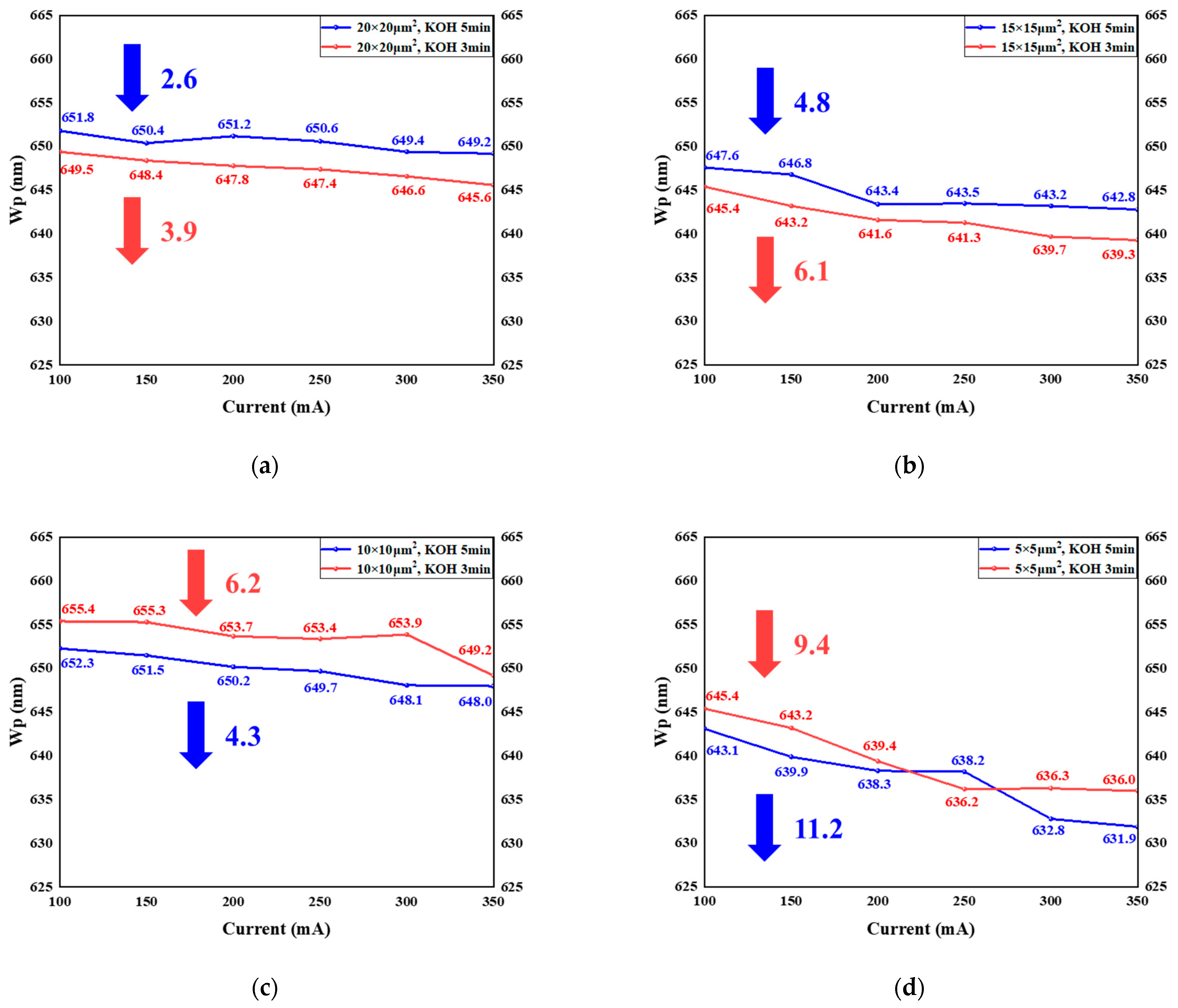
Figure 7 demonstrates the blue shift characteristics of red-emitting μLED arrays with varying pixel sizes under different KOH wet treatment conditions, and provides a summarized representation of the data, focusing on the relationship between the Wp and the injection current, with arrows indicating the specific values of the blue shift. From the data, it is evident that within the tested injection current range, for arrays with pixel sizes of 20 and 15 µm, the samples subjected to 5 min of KOH wet treatment exhibit a higher Wp compared to those treated for 3 min. In contrast, for arrays with smaller pixel sizes (e.g., 10 and 5 µm), the samples treated for 3 min display relatively higher Wp values. For arrays of the same pixel size, despite the variation in wet treatment time, the difference in Wp is minimal, with a maximum variation of 5.8 nm. As the injection current increases, all arrays show a general reduction in Wp, consistent with the typical blue shift observed in red μLEDs. Notably, all arrays maintain excellent wavelength uniformity, which suggests that the epitaxial layers used in this study exhibit superior structural quality and growth characteristics, effectively mitigating the quantum-confined Stark effect and minimizing the extent of the blue shift. Further analysis of the Wp shift values reveals that, except for the 5 µm pixel array, the other arrays exhibit more pronounced blue shift effects under the 3-min KOH wet treatment condition. This indicates that a properly extended wet treatment time can mitigate the blue shift effect in red μLED arrays. However, for arrays with very small pixel sizes, due to their higher surface-to-volume ratio, excessive wet treatment may result in over-etching, which could degrade their performance.
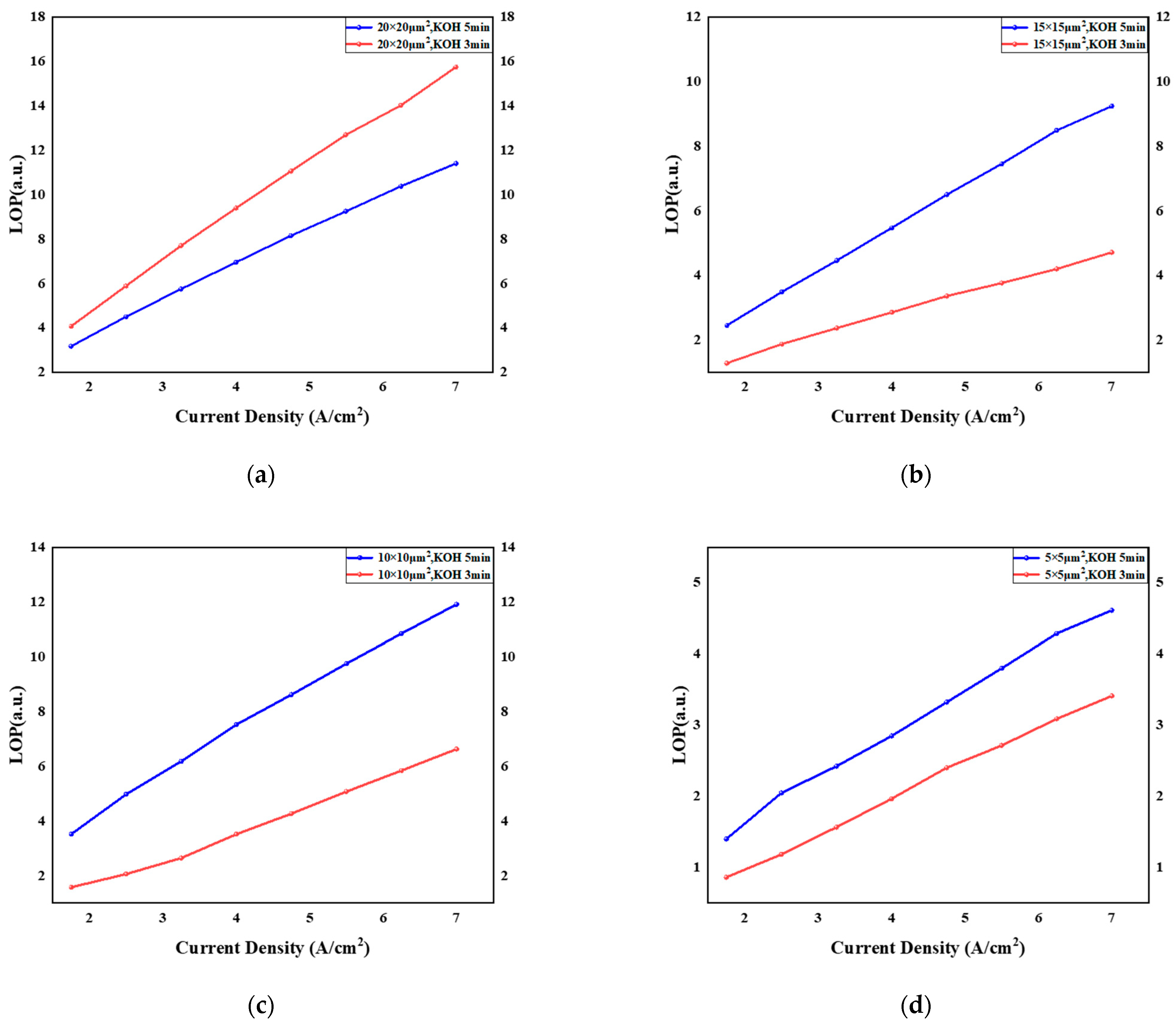
Figure 8 investigates the relationship between light output power (LOP) and injection current density for μLED arrays with different pixel sizes subjected to varying KOH wet treatment times. It should be clarified that the LOP values presented in this study are relative. The data show a monotonic increase in LOP with the current density injection for all arrays. For arrays with pixel sizes of 15, 10, and 5 µm, the LOP is higher under the 5-min KOH wet treatment. This can be attributed to the more efficient reduction in leakage current compared to the 3-min one, which effectively mitigates leakage current pathways and enhances the effective recombination of charge carriers. However, for the 20 µm pixel arrays, although the I-V curves in
Figure 5 and
Figure A1 indicate a lower leakage current for the 5-min treatment, the relatively larger surface area may result in a deterioration of the electrode-GaN interface during prolonged wet treatment. This degradation can limit the injection efficiency of charge carriers, thus constraining the overall enhancement of light output power.
Figure 9 demonstrates the relationship between relative optoelectronic efficiency and injection current density for arrays with varying pixel sizes, subjected to different KOH wet treatment times. It is important to emphasize that the efficiency discussed here is defined as the light output power divided by the electrical power, and it refers to relative efficiency. As illustrated, the efficiency of all arrays decreases monotonically with increasing injection current density, a characteristic behavior associated with the Droop effect commonly observed in red μLEDs. This phenomenon arises primarily due to a reduction in carrier migration rates and recombination efficiency at high current densities, leading to an increase in non-radiative recombination. Consequently, carriers fail to efficiently recombine and are dissipated as heat or undergo unintended recombination processes. For arrays with pixel sizes of 15, 10, and 5 μm, those subjected to 5 min of KOH wet treatment exhibit higher optical efficiency. This enhancement is attributed to the more effective reduction of surface and sidewall defects, particularly the density of dangling bonds, which diminishes non-radiative recombination and promotes more efficient carrier recombination. As a result, the photon conversion efficiency from recombined carriers is enhanced. Conversely, for the 20 μm pixel arrays, the efficiency after 5 min of wet treatment is lower, primarily due to a decrease in light output power, as discussed earlier. For arrays with pixel sizes of 10 and 5 μm, the efficiency decreases more rapidly after 5 min of wet treatment. This is likely due to the introduction of localized stress, especially in smaller structures, as a result of prolonged treatment. The wet treatment process may lead to uneven stress distribution on the surface and sidewalls, which can distort the electric field distribution in the quantum wells, ultimately affecting carrier behavior and recombination efficiency. Addressing this issue may require optimizing the material growth process to mitigate the effects of stress on both electrical and optical performance. Notably, μLED arrays with extremely small pixel sizes (5 μm) exhibit superior optical efficiency. We hypothesize that the wet treatment process not only effectively removes surface defects but also enhances crystal quality. Furthermore, the surface roughening induced by wet treatment improves light extraction efficiency, particularly from the sidewalls, reducing optical losses due to reflection, scattering, and absorption during light transmission. This results in an overall enhancement in optical efficiency. This approach provides valuable insights for improving the efficiency of ultra-small pixel size red μLED arrays.
4. Conclusions
We successfully fabricated GaN-based red μLED arrays with pixel sizes ranging from 5 to 20 μm, systematically investigating the effects of 3-min and 5-min KOH wet treatments on their morphology and optoelectronic properties. Due to the non-emissive nature of the arrays that were not treated by KOH, they were excluded from the scope of the work’s analysis. Scanning electron microscopy analysis revealed that both treatments improved surface morphology, reducing defects introduced by ICP dry etching. The 5-min treatment exhibited superior results in terms of surface optimization. In electrical performance, the 5-min KOH treatment significantly reduced leakage current, decreasing by two orders of magnitude compared to the 3-min treatment. Optical characterization revealed that Wp and FWHM correspond to standard red emission, with minimal impact from the varying wet treatment time. The blue shift was negligible across all arrays, and wavelength uniformity was maintained, suggesting that the epitaxial material used exhibited excellent quality and growth characteristics. While the 5-min KOH treatment mitigated the blue shift in red μLED arrays, the 5 μm arrays showed an exacerbated blue shift with prolonged treatment, indicating that longer time may negatively affect smaller arrays. In terms of light output power, all arrays showed a monotonic increase with rising injection current density, except for the 20 μm arrays. For the 15, 10, and 5 μm arrays, the 5-min KOH treatment resulted in higher LOP, while the 20 μm arrays experienced a reduction in LOP due to decreased electrode-GaN layer contact quality, which limited carrier injection. Regarding optoelectronic efficiency, all arrays exhibited the droop effect. The 5-min KOH treatment improved efficiency for the vast majority arrays except for the 20 μm arrays. This suggests that the KOH treatment effectively suppresses surface non-radiative recombination and plasma-induced defects. The rapid efficiency decreases in the 10 and 5 μm arrays treated for 5 min indicates a need for further optimization of the epitaxial growth process. Notably, the 5 μm pixel arrays exhibited exceptional optoelectronic efficiency, likely due to the combined effects of defect passivation and surface roughening, which enhanced crystal quality and reduced optical losses, thereby improving overall performance.
This work demonstrates the successful fabrication of GaN-based red μLED arrays of varying pixel sizes and provides valuable insights into the impact of KOH wet treatment on array morphology and optoelectronic performance. Our findings contribute to the development of high-performance GaN-based red μLED arrays and offer guidance for optimizing small-pixel array fabrication for improved performance and stability.


