Article

Design of GaN-Based Laser Diode Structures with Nonuniform Doping Distribution in a p-AlGaN Cladding Layer for High-Efficiency Operation

Department of Physics, Inha University, 100 Inha-ro, Michuhol-gu, Incheon 22212, Republic of Korea
*
Author to whom correspondence should be addressed.
Crystals 2025, 15(3), 259; https://doi.org/10.3390/cryst15030259
Submission received: 20 February 2025 / Revised: 7 March 2025 / Accepted: 10 March 2025 / Published: 11 March 2025
(This article belongs to the Special Issue II-VI and III-V Semiconductors for Optoelectronic Devices)

Abstract

:
In GaN-based laser diode (LD) structures, it is essential to optimize the doping concentration and profiles in p-type-doped layers because of the trade-off between laser power and operation voltage as the doping concentration varies. In this study, we proposed GaN-based blue LD structures with nonuniform doping distributions in the p-AlGaN cladding layer to reduce the modal loss and demonstrated improved efficiency characteristics using numerical simulations. We compared the laser power, operation voltage, and wall-plug efficiency (WPE) of LDs with uniform, linear, and quadratic doping profiles in the p-AlGaN cladding layer. As the doping concentration becomes increasingly inhomogeneous, the laser output power increases significantly because of the reduced overlap of the laser mode with the p-AlGaN cladding layer. However, this nonuniform doping profile also leads to an increase in the operation voltage due to the expansion of the low-doping region. By optimizing the nonuniform doping distribution in the p-type cladding layer, the WPE was found to be improved by over 5% compared to a conventional uniformly doped p-cladding layer. The proposed design of LD structures is expected to enhance the efficiency of high-power GaN-based LDs.

1. Introduction

High-power blue laser diodes (LDs) based on InGaN/GaN materials have gained significant attention for various applications including projection displays [1,2,3], laser-based white lighting [4,5,6], free-space communications [7,8,9], and laser processing of materials [10,11,12,13]. The high light absorption coefficient of Cu in the blue wavelengths has led to an increasing demand for high-power blue LDs for Cu-based material processing [11,13]. In recent years, there have been considerable improvements in the performance of blue LDs, with laser output power exceeding 6 W, threshold current density (Jth) below 1 kA/cm2, slope efficiency (SE) surpassing 2 W/A, and wall-plug efficiency (WPE) exceeding 40% [2,3,11,12,13,14,15].
Though the development of high-power and high-efficiency blue LDs has made remarkable advancements, the WPE of InGaN blue LDs is still limited to around 50%. The low conductivity of Mg-doped p-type layers is one of the major factors limiting the WPE of GaN-based LDs [16,17,18,19]. Owing to the high acceptor activation energy of Mg in (Al)GaN and the low mobility of hole carriers, the electrical resistivity of Mg-doped p-type-doped layers is significantly higher than that of n-type-doped layers, which results in a high operation voltage. To improve the conductivity of the p-AlGaN cladding, high-concentration Mg doping is required to increase the hole concentration.
Meanwhile, heavily doped p-type layers lead to increased optical absorption in GaN-based LDs via free-carrier absorption [20,21]. Because of the higher doping concentration in the p-type region, the p-type layers experience more significant optical absorption loss compared to the n-type layers. The absorption coefficient of p-type layers in GaN-based LDs has been reported to be in the range of several tens of cm−1 [22,23,24,25], which can significantly decrease the SE and, consequently, the laser output power of the LD. To mitigate the modal loss associated with p-type doping, the waveguide layer positioned above the multiple-quantum-well (MQW) active layers is typically left undoped [25,26,27,28]. Another strategy employed an asymmetric laser mode distribution, where the peak intensity of the laser mode is shifted toward the n-type layers to reduce the overlap of the laser mode with the p-type cladding layer [29,30]. However, the optical confinement factor (OCF) in the MQW layers can be significantly reduced in strongly asymmetric structures, leading to an increased lasing threshold.
In this paper, we propose a new design for a GaN-based LD structure with an inhomogeneous doping distribution in the p-type cladding layer to decrease modal loss and demonstrate improved efficiency characteristics through numerical simulations. In our proposed design, the doping concentration decreases as the position in the p-type cladding layer moves toward the MQW active region. This doping distribution helps decrease the overlap of the laser mode with the p-type-doped region while maintaining a constant average doping concentration in the p-cladding layer, resulting in reduced modal loss and an increase in SE. However, the region of low doping density can be increased by the inhomogeneous doping distribution, which could lead to an increase in the operation voltage. Therefore, optimizing the doping profile in the p-type cladding region is needed to achieve the best efficiency.
For the simulation of this study, we utilized the simulation software laser technology integrated program (LASTIP) developed by Crosslight [31]. LASTIP has been extensively applied for the numerical exploration of semiconductor laser characteristics. In this research, we compare the laser power, voltage, and WPE characteristics for uniform, linear, and quadratic doping profiles in the p-type cladding region and discuss the optimum doping conditions in order to achieve high-WPE operation.

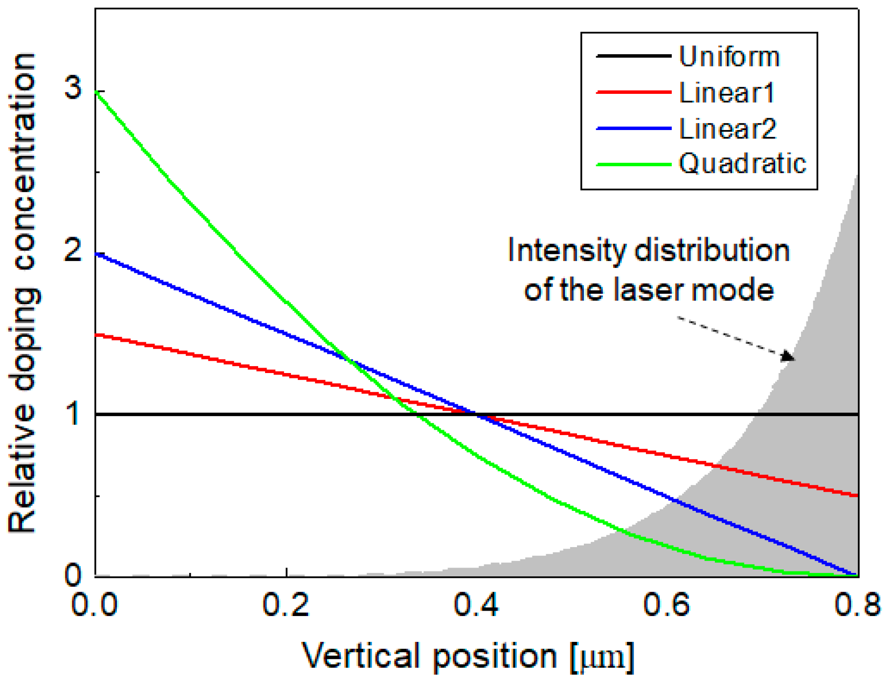
2. Simulation Structure and Methods

Figure 1a depicts the side view of the InGaN blue LD structure used in this study. The epitaxial layers are similar to those used in our previous works [18,32]. The layer structure consisted of an n-Al0.04Ga0.96N cladding layer, a lower n-GaN waveguide layer, MQW active region, an upper GaN waveguide layer, a p-Al0.2Ga0.8N electron-blocking layer (EBL), a p-Al0.05Ga0.95N cladding layer, and a p-GaN contact layer. The active region included two 3 nm thick In0.15Ga0.85N quantum wells (QWs) with a 10 nm In0.02Ga0.98N barrier layer. With this MQW structure, the LD emits light at a peak wavelength of 450 nm at 25 °C. The thicknesses of the n-AlGaN and p-AlGaN layers were set to 1.2 and 0.8 μm, respectively. Both the lower and upper GaN waveguide layers have a thickness of 200 nm, which was chosen to achieve a high OCF and, consequently, a low threshold current [18]. The ridge width and cavity length of the simulated LD structures were chosen to be 10 and 1200 μm, respectively. The reflectance of the front and rear mirrors was assumed to be 5% and 98%, respectively.
The active region contained undoped QW and barrier layers. The doping concentration of both the n-AlGaN cladding and n-GaN lower waveguide layers was set to 5 × 1018 cm−3. The upper waveguide layer was undoped to minimize the optical absorption loss that could arise from p-type doping. The Mg doping concentration of the p-AlGaN EBL was set to 4 × 1019 cm−3 based on our previous simulation results [18]. The doping concentration of the p-AlGaN cladding layer varied with the position within the cladding layer, and the average doping concentration of the p-AlGaN cladding layer varied in the range from 1 × 10¹⁹ to 4 × 1019 cm−3. It should be noted that the actual concentration of hole carriers in the p-type region would be significantly lower than the Mg doping concentration owing to its high acceptor activation energy. According to the incomplete ionization model presented in Ref. [18], the ratio of Mg ionization was evaluated to be only about 1 percent.
Using LASTIP software, the LD device characteristics were investigated, including the relationship between laser output power and current (L-I curve) and the relationship between forward voltage and current (V-I curve). It solves the InGaN QW band structures, carrier drift and diffusion equations, and carrier recombination models in a self-consistent manner [31]. In addition, we incorporated the internal polarization fields caused by spontaneous and piezoelectric fields in (Al)GaN and (In)GaN layers. The polarization fields were modeled based on Ref. [33], assuming that the polarization field was reduced to 25% of its theoretical value by screening effects [28,34]. The mobility of hole carriers in InGaN, GaN, and AlGaN materials was set to be 5, 10, and 15 cm2/Vs, respectively [31,35]. As mentioned before, the high activation energy of Mg acceptors in the p-type layers causes incomplete ionization. This was taken into account in the simulation using the incomplete ionization model. The ionization energy of acceptor ions in GaN and AlGaN layers increased linearly from 170 meV (GaN) to 470 meV (AlN) [16,35]. This resulted in an acceptor ionization energy of 180 and 230 meV for the p-Al0.05Ga0.95N cladding and p-Al0.2Ga0.8N EBL, respectively.
Figure 1b shows the profiles of the refractive index and wave intensity of the lasing mode. The refractive indices of GaN, Al0.05GaN, and Al0.2GaN layers were set to 2.444, 2.417, and 2.368, respectively, using the refractive index formula for AlGaN and InGaN alloys at 450 nm in Refs. [36,37]. As shown in Figure 1b, the lasing mode is symmetrically distributed and centered at the QW layers. In this case, the OCF of the laser was calculated to be ~1.5%. To determine the optical absorption loss caused by free-carrier absorption, we employed a first-principle model in Ref. [21], which showed an absorption cross-section of ~0.6 × 10⁻¹⁸ and ~0.9 × 10⁻¹⁸ cm2 for n-type- and p-type-doped layers, respectively [32].
In the model for carrier recombination in LASTIP, the radiative recombination rate is determined by integrating the spontaneous emission spectrum with a Lorentzian line-shape function. The lasing threshold of InGaN blue LDs is significantly affected by the Auger recombination coefficient (C) [17,38]. In our simulation, we set C to 2 × 1030 cm−6/s to obtain a threshold current density of approximately 1 kA/cm2, similar to values observed in high-performance blue LDs [2,11,14,15]. In the simulation of this study, the LD temperature was fixed at 25 °C, and no self-heating effects were taken into account, implying that the simulation results reflected the pulsed operation mode without thermal effects.

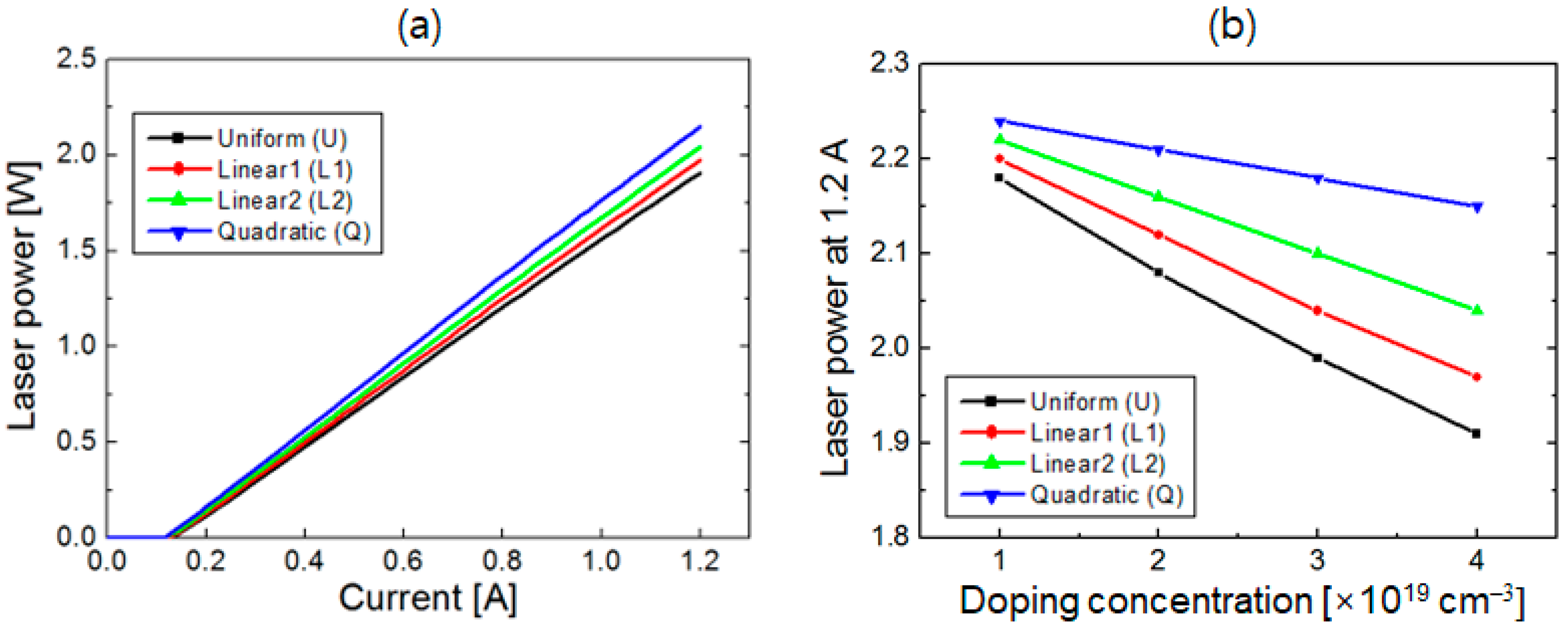
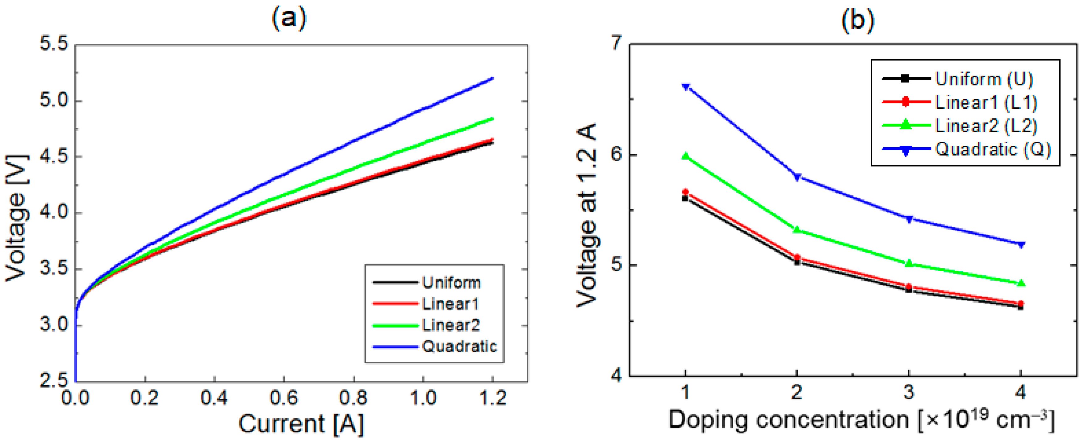
3. Results and Discussion

Figure 2 illustrates four types of doping concentration distributions considered in this study as a function of the position in the p-type cladding layer: uniform (U), linear1 (L1), linear2 (L2), and quadratic (Q). The “uniform” distribution (U) maintains a constant doping concentration throughout the p-cladding layer, which is the case with the conventional LD structure. The “linear1” (L1) and “linear2” (L2) distributions exhibit a linear decrease in doping concentration as the distance increases from the p-contact layer to the u-GaN waveguide layer. Specifically, for L1, the doping concentration decreases from 1.5 times to 0.5 times the average concentration, while for L2, it decreases from 2 times the average concentration to 0. The “quadratic” (Q) distribution is characterized by a doping concentration that declines according to a quadratic function as the distance from the p-contact layer increases, with concentrations decreasing from three times the average concentration to zero. Thus, the degree of nonuniformity in doping concentration increases in the following order: U, L1, L2, and Q. For all four doping distributions in Figure 2, the average doping concentration remains the same. The shaded area in Figure 2 represents the intensity distribution of the laser mode. It is evident that the overlap between the laser mode and doping concentration decreases in the order of U, L1, L2, and Q, implying that the modal loss in the p-cladding layer can be reduced as the doping concentration distribution becomes more inhomogeneous.
The gradient doping profiles, as illustrated in Figure 2, have been mainly reported in GaAs-based materials [39,40], and there are few experimental reports on nitride materials utilizing the gradient doping profiles. Instead, AlGaN-/GaN-based optoelectronic and electronic devices have frequently employed modulation doping or delta doping profiles, where the doping concentration periodically changes rapidly in a short distance. For instance, the variation in Mg doping concentration was ~1019 cm−3 within a 20 nm range in the AlGaN layer [41,42,43]. Therefore, it would not be challenging to experimentally implement the gradient doping profiles investigated in this study.
Figure 3a shows the simulation results of the L-I curves for the four doping distributions, U, L1, L2, and Q, with an average doping concentration of 4 × 1019 cm−3. It can be seen that, for the same current, the laser power increased in the order of U, L1, L2, and Q. This sequence aligns with the trend observed in Figure 2, where the lower doping concentrations are found in the p-cladding region close to the u-GaN waveguide layer. This indicates that, as the overlap between the laser mode and the doping concentration decreases, the absorption of laser light also decreases, resulting in an increase in laser output power. In Figure 3b, the laser power at an injection current of 1.2 A is plotted as a function of the average doping concentration, ranging from 1 × 10¹⁹ to 4 × 1019 cm−3 for the four doping distributions. For each average doping concentration, the laser power again follows the following order: U, L1, L2, and Q. As the doping concentration increased, the laser power declined more rapidly in the sequence of Q, L2, L1, and U. Specifically, as the doping concentration increased from 1 × 10¹⁹ to 4 × 1019 cm−3, the laser power of U decreased by 0.25 W, while that of Q decreased by only 0.08 W. This is attributed to the decreasing overlap between the p-type doping concentration, and the laser mode as the doping distribution becomes increasingly inhomogeneous.
Figure 4a shows the simulation results of the V-I curves for the four doping distributions of the p-cladding layer when the average doping concentration is 4 × 1019 cm−3. For a given current, the operation voltages of the distributions U and L1 were nearly identical, while the voltage for distribution L2 increased slightly compared to U. In contrast, the operation voltage for the case of Q shows a significant increase when compared to uniform and linear distributions. In Figure 4b, the voltage of the four doping distributions is plotted as a function of the average doping concentration when the injection current is 1.2 A. The voltage decreased with increasing doping concentration due to the increased conductivity of the p-cladding layer. For any specific doping concentration, the operation voltage increased in the order of U, L1, L2, and Q. The difference in voltage between U and Q decreased from 1.1 to 0.7 V as the average doping concentration increased from 1 × 10¹⁹ and 4 × 1019 cm−3. As shown in Figure 2, the region of low doping density expands with increasing nonuniformity of the doping concentration distribution, resulting in an overall increase in the overall resistance of the p-cladding layer, which in turn leads to higher operation voltage.
The results presented in Figure 3 and Figure 4 indicate a trade-off relation between laser power and voltage as the doping distribution varied. As the doping distribution becomes more inhomogeneous, the laser power increases due to reduced optical loss, while the voltage decreases because of the increased resistance in the p-cladding layer. Figure 5 shows the WPE as a function of current for the four doping distributions when the average doping concentration of the p-cladding layer is 2 × 10¹⁹ and 4 × 1019 cm−3. The WPE values were obtained from the results of the L-I curves in Figure 2 and the V-I curves in Figure 3. When the average doping concentration is 2 × 1019 cm−3, the WPE of L1 is the highest, and that of Q is the lowest in most current ranges. On the contrary, when the average doping concentration is 4 × 1019 cm−3, distribution Q has the highest WPE for currents below 0.8 A, whereas distributions L1 and L2 show the highest WPE for currents above 0.8 A. Throughout all current ranges, distribution U has the lowest WPE.
Figure 6a shows the maximum WPE values for the four doping distributions as a function of the average doping concentration in the p-AlGaN cladding layer. The optimal doping profile for achieving the highest WPE is dependent on the average doping concentration in the p-AlGaN cladding layer. For an average doping concentration of 2 × 1019 cm−3 or lower, distribution L1 shows the highest maximum WPE. At an average doping concentration of 3 × 1019 cm−3, both L1 and L2 show the maximum WPE. When the average doping concentration increases to 4 × 1019 cm−3, distribution Q exhibits the highest maximum WPE. For the uniform doping distribution, the maximum WPE was limited to 36.7%. Compared to this, the nonuniform doping distributions demonstrated improved maximum WPEs: L1, L2, and Q achieved 37.2%, 37.1%, and 37.3%, respectively.
Figure 6b compares the maximum WPE of the four doping distributions relative to that of the uniform doping distribution. As the average doping concentration increases, the greater the nonuniformity of the doping distribution (in the order of L1, L2, and Q), the larger the variation in the maximum WPE. At an average doping concentration of 4 × 1019 cm−3, the maximum WPE of the quadratic doping distribution increased by more than 5% compared to that of the conventional uniform distribution. This indicates that employing a nonuniform doping distribution in the p-cladding layer can be beneficial for enhancing the efficiency characteristics of GaN-based blue LDs.

4. Conclusions

In this work, we proposed GaN-based LD structures with inhomogeneous doping distributions in the p-AlGaN cladding layer to reduce the modal loss while maintaining average doping concentration. Numerical simulations were conducted to compare the effects of uniform, linear, and quadratic doping profiles on laser power, operation voltage, and WPE. As the doping concentration decreased more rapidly toward the MQW active region, the laser output power increased as a result of the reduced overlap of the laser mode with a heavily doped p-cladding layer. However, the operation voltage also increased because of the expanded low-doping region. It was found that optimizing the nonuniform doping distribution in the p-cladding layer could enhance the WPE by more than 5% compared to the conventional uniformly doped p-cladding layer. The presented design of the LD structures is expected to provide valuable insights into improving the efficiency of high-power blue LDs.

Author Contributions

Conceptualization, H.-Y.R.; methodology, C.O. and H.-Y.R.; software, C.O. and H.-Y.R.; validation, H.-Y.R.; investigation, C.O.; data curation, C.O.; writing—original draft preparation, C.O.; writing—review and editing, H.-Y.R.; supervision, H.-Y.R.; project administration, H.-Y.R.; funding acquisition, H.-Y.R. All authors have read and agreed to the published version of the manuscript.

Funding

This research was supported by the Basic Science Research Program through the National Research Foundation of Korea (NRF) funded by the Ministry of Education (2022R1A6A1A03051705) and by the INHA University Research Grant.

Data Availability Statement

The data supporting the findings of this paper are available from the corresponding authors upon reasonable request.

Conflicts of Interest

The authors declare no conflicts of interest.

References

  1. Ponce, F.A.; Bour, D.P. Nitride-based semiconductors for blue and green light-emitting devices. Nature 1997, 386, 351–359. [Google Scholar] [CrossRef]
  2. Murayama, M.; Nakayama, Y.; Yamazaki, K.; Hoshina, Y.; Watanabe, H.; Fuutagawa, N.; Kawanishi, H.; Uemura, T.; Narui, H. Watt-class green (530 nm) and blue (465 nm) laser diodes. Phys. Status Solidi A 2018, 215, 1700513. [Google Scholar] [CrossRef]
  3. Nakatsu, Y.; Nagao, Y.; Hirao, T.; Hara, Y.; Masui, S.; Yamamoto, T.; Nagahama, S. Blue and green InGaN semiconductor lasers as light sources for displays. Proc. SPIE 2020, 11280, 81–87. [Google Scholar]
  4. Wierer, J.J.; Tsao, J.Y.; Sizov, D.S. Comparison between blue lasers and light-emitting diodes for future solid-state lighting. Laser Photonics Rev. 2013, 7, 963–993. [Google Scholar] [CrossRef]
  5. Ryu, H.Y.; Kim, D.H. High-brightness phosphor-conversion white light source using InGaN blue laser diode. J. Opt. Soc. Korea 2010, 14, 415–419. [Google Scholar] [CrossRef]
  6. Sui, P.; Lin, H.; Lin, Y.; Lin, S.; Huang, J.; Xu, J.; Cheng, Y.; Wang, Y. Toward high-power-density laser-driven lighting: Enhancing heat dissipation in phosphor-in-glass film by introducing h-BN. Opt. Lett. 2022, 47, 3455–3458. [Google Scholar] [CrossRef] [PubMed]
  7. Watson, S.; Tan, M.; Najda, S.P.; Perlin, P.; Leszczynski, M.; Targowaski, G.; Grzanka, S.; Kelly, A.E. Visible light communications using a directly modulated 422 nm GaN laser diode. Opt. Lett. 2013, 38, 3792–3794. [Google Scholar] [CrossRef]
  8. Lee, C.; Zhang, C.; Cantore, M.; Farrell, R.M.; Oh, S.H.; Margalith, T.; Speck, J.S.; Nakamura, S.; Bowers, J.E.; DenBaars, S.P. 4 Gbps direct modulation of 450 nm GaN laser for high-speed visible light communication. Opt. Express 2015, 23, 16232–16237. [Google Scholar] [CrossRef]
  9. Wu, T.C.; Chi, Y.C.; Wang, H.Y.; Tsai, C.T.; Lin, G.R. Blue laser diode enables underwater communication at 12.4 Gbps. Sci. Rep. 2017, 7, 40480. [Google Scholar] [CrossRef]
  10. Wang, H.; Kawahito, Y.; Yoshida, R.; Nakashima, Y.; Shiokawa, K. Development of a high-power blue laser (445 nm) for material processing. Opt. Lett. 2017, 42, 2151–2154. [Google Scholar] [CrossRef]
  11. Baumann, M.; Balck, A.; Malchus, J.; Chacko, R.V.; Marfels, S.; Witte, U.; Dinakaran, D.; Ocylok, S.; Weinbach, M.; Bachert, C. 1000 W blue fiber-coupled diode laser emitting at 450 nm. Proc. SPIE 2019, 10900, 10–21. [Google Scholar]
  12. Hagino, H.; Kawaguchi, M.; Nozaki, S.; Mochida, A.; Kano, T.; Takigawa, S.; Katayama, T.; Tanaka, T. High-power InGaN laser array with advanced lateral-corrugated waveguides. IEEE J. Quantum Electron. 2021, 57, 2600107. [Google Scholar] [CrossRef]
  13. Hatakeyama, K.; Tanahashi, Y.; Konishi, R.; Nakagaki, M.; Okuno, R.; Sugiyama, T.; Shibuya, S.; Okada, A.; Hayamizu, N. High-power and high-luminance blue laser module using GaN-based laser diodes. Proc. SPIE 2024, 12867, 74–80. [Google Scholar]
  14. Zhong, Z.; Lu, S.; Li, J.; Lin, W.; Huang, K.; Li, S.; Cai, D.; Kang, J. Design and fabrication of high power InGaN blue laser diode over 8 W. Opt. Laser Technol. 2021, 139, 106985. [Google Scholar] [CrossRef]
  15. Zhang, Z.; Yang, J.; Liang, F.; Chen, P.; Liu, Z.; Zhao, D. Low threshold current density and high power InGaN-based blue-violet laser diode with an asymmetric waveguide structure. Opt. Express 2023, 31, 7839–7849. [Google Scholar] [CrossRef] [PubMed]
  16. Piprek, J. Comparative efficiency analysis of GaN-based light-emitting diodes and laser diodes. Appl. Phys. Lett. 2016, 109, 021104. [Google Scholar] [CrossRef]
  17. Piprek, J. Analysis of efficiency limitations in high-power InGaN/GaN laser diodes. Opt. Quantum Electron. 2016, 48, 471. [Google Scholar] [CrossRef]
  18. Onwukaeme, C.; Ryu, H.Y. Investigation of the optimum Mg doping concentration in p-type-doped layers of InGaN blue laser diode structures. Crystals 2021, 11, 1335. [Google Scholar] [CrossRef]
  19. Aktas, M.; Kafar, A.; Stanczyk, S.; Marona, L.; Schiavon, D.; Grzanka, S.; Wisniewski, P.; Perlin, P. Optimization of p-clading layer utilizing polarization doping for blue-violet InGaN laser diodes. Opt. Laser Technol. 2024, 177, 111144. [Google Scholar] [CrossRef]
  20. Schubert, E.F. Light-Emitting Diodes, 2nd ed.; Cambridge University Press: Cambridge, UK, 2006; pp. 145–149. [Google Scholar]
  21. Kioupakis, E.; Rinke, P.; Van de Walle, C.G. Determination of internal loss in nitride lasers from first principles. Appl. Phys. Express 2010, 3, 082101. [Google Scholar] [CrossRef]
  22. Son, J.K.; Lee, S.N.; Paek, H.S.; Sakong, T.; Kim, H.K.; Park, Y.; Ryu, H.Y.; Nam, O.H.; Hwang, J.S.; Cho, Y.H. Measurement of optical loss variation on thickness of InGaN optical confinement layers of blue-violet-emitting laser diodes. J. Appl. Phys. 2008, 103, 103101. [Google Scholar] [CrossRef]
  23. Kioupakis, E.; Rinke, P.; Schleife, A.; Bechstedt, F.; Van de Walle, C.G. Free-carrier absorption in nitrides from first principles. Phys. Rev. B 2010, 82, 241201. [Google Scholar] [CrossRef]
  24. Chen, Y.; Jiang, D.; Zeng, C.; Xu, C.; Sun, H.; Hou, Y.; Zhou, M. Controlling GaN-based laser diode performance by variation of the Al content of an inserted AlGaN electron blocking layer. Nanomaterials 2024, 14, 449. [Google Scholar] [CrossRef]
  25. Uchida, S.; Takeya, M.; Ikeda, S.; Mizuno, T.; Fujimoto, T.; Matsumoto, O.; Goto, S.; Tojyo, T.; Ikeda, M. Recent progress in high-power blue-violet lasers. IEEE J. Sel. Top. Quantum Electron. 2023, 9, 1252. [Google Scholar] [CrossRef]
  26. Liang, F.; Zhao, D.; Jiang, D.; Liu, Z.; Zhu, J.; Chen, P.; Yang, J.; Liu, W.; Li, X.; Liu, S.; et al. New design of upper waveguide with unintentionally doped InGaN layer for InGaN-based laser diode. Opt. Laser Technol. 2017, 97, 284–289. [Google Scholar] [CrossRef]
  27. Chen, P.; Feng, M.X.; Jiang, D.S.; Zhao, D.G.; Liu, Z.S.; Li, L.; Wu, L.L.; Le, L.C.; Zhu, J.J.; Wang, H. Improvement of characteristics of InGaN-based laser diodes with undoped InGaN upper waveguide layer. J. Appl. Phys. 2012, 112, 113105. [Google Scholar] [CrossRef]
  28. Hou, Y.; Zhao, D.; Liang, F.; Liu, Z.; Yang, J.; Chen, P. Enhancing the efficiency of GaN-based laser diodes by the designing of a p-AlGaN cladding layer and an upper waveguide layer. Opt. Mater. Express 2021, 11, 1780. [Google Scholar] [CrossRef]
  29. Ryu, H.Y.; Ha, K.H.; Lee, S.N.; Choi, K.K.; Jang, T.; Son, J.K.; Chae, J.H.; Chae, S.H.; Paek, H.S.; Sung, Y.J.; et al. Single-mode blue-violet laser diodes with low beam divergence and high COD level. IEEE Photonics Technol. Lett. 2006, 18, 1001–1003. [Google Scholar] [CrossRef]
  30. Ryu, H.Y.; Ha, K.H.; Son, J.K.; Paek, H.S.; Sung, Y.J.; Kim, K.S.; Kim, H.K.; Park, Y.; Lee, S.N.; Nam, O.H. Comparison of output power of InGaN laser diodes for different Al compositions in the AlGaN n-cladding layer. J. Appl. Phys. 2009, 105, 103102. [Google Scholar] [CrossRef]
  31. LASTIP by Crosslight Software Inc. Burnaby Canada. Available online: http://crosslight.com (accessed on 1 January 2025).
  32. Onwukaeme, C.; Ryu, H.Y. Optimum design of InGaN blue laser diodes with indium-tin-oxide and dielectric cladding layers. Nanomaterials 2024, 14, 1409. [Google Scholar] [CrossRef]
  33. Fiorentini, V.; Bernardini, F.; Ambacher, O. Evidence for nonlinear macroscopic polarization in III-V nitride alloy heterostructures. Appl. Phys. Lett. 2002, 80, 1204–1206. [Google Scholar] [CrossRef]
  34. Wang, W.; Li, D.; Liu, N.; Chen, Z.; Wang, L.; Liu, L.; Li, L.; Wan, C.; Chen, W.; Hu, X.; et al. Improvement of hole injection and electron overflow by a tapered AlGaN electron blocking layer in InGaN-based blue laser diodes. Appl. Phys. Lett. 2012, 100, 031105. [Google Scholar]
  35. Piprek, J. Semiconductor Optoelectronic Devices; Academic Press: London, UK, 2003; pp. 187–211. [Google Scholar]
  36. Bergmann, M.J.; Casey, H.C., Jr. Optical-field calculations for lossy multiple-layer AlxGa1−xN/InxGa1−xN laser diodes. J. Appl. Phys. 1998, 84, 1196–1203. [Google Scholar] [CrossRef]
  37. Laws, G.M.; Larkins, E.C.; Harrison, I.; Molloy, C.; Somerford, D. Improved refractive index formulas for the AlxGa1−xN and InyGa1−yN alloys. J. Appl. Phys. 2001, 89, 1108–1115. [Google Scholar] [CrossRef]
  38. Ryu, H.Y. Investigation into the anomalous temperature characteristics of InGaN double quantum well blue laser diodes using numerical simulation. Nanoscale Res. Lett. 2017, 12, 366. [Google Scholar] [CrossRef] [PubMed]
  39. Zhao, Y.; Liang, P.; Ren, H.; Han, P. Enhanced efficiency in 808 nm GaAs laser power converters via gradient doping. AIP Adv. 2019, 9, 105206. [Google Scholar] [CrossRef]
  40. Jakiela, R.; Barcz, A. Diffusion and activation of Si implanted into GaAs. Vacuum 2003, 70, 97–101. [Google Scholar] [CrossRef]
  41. Chen, Y.; Wu, H.; Han, E.; Yue, G.; Chen, Z.; Wu, Z.; Wang, G.; Jiang, H. High hole concentration in p-type AlGaN by indium-surfactant-assisted Mg-delta doping. Appl. Phys. Lett. 2015, 106, 162102. [Google Scholar] [CrossRef]
  42. Wu, Z.; Zhang, X.; Dai, Q.; Zhao, J.; Fan, A.; Wang, S.; Cui, Y. High hole concentration in nonpolar a-plane p-AlGaN films with Mg-delta doping technique. Superlattice Microst. 2017, 109, 880–885. [Google Scholar] [CrossRef]
  43. Hertkorn, J.; Thapa, S.B.; Wunderer, T.; Scholz, F.; Wu, Z.H.; Wei, Q.Y.; Ponce, F.A.; Moram, M.A.; Humphreys, C.J.; Vierheilig, C.; et al. Highly conductive modulation doped composition graded p-AlGaN/(AlN)/GaN multiheterostructures grown by metalorganic vapor phase epitaxy. J. Appl. Phys. 2009, 106, 013720. [Google Scholar] [CrossRef]
Figure 1. (a) Schematic of the simulated LD structure. (b) Vertical profiles of the refractive index (left vertical axis) and normalized wave intensity of the lasing mode (right vertical axis). The origin of the vertical position corresponds to the interface between the p-GaN contact and p-AlGaN cladding layer.
Crystals 15 00259 g001
Figure 2. Doping concentration distributions considered in this study as a function of the position in the p-AlGaN cladding layer: uniform (U), linear1 (L1), linear2 (L2), and quadratic (Q). The shaded area represents the intensity distribution of the laser mode. The overlap between the laser mode and doping concentration decreases in the order of U, L1, L2, and Q.
Crystals 15 00259 g002
Figure 3. (a) Simulated laser power versus current (L-I) curves for the four doping distributions, U, L1, L2, and Q, when the average doping concentration is 4 × 1019 cm−3. (b) Laser power at an injection current of 1.2 A plotted as a function of the average doping concentration for the four doping distributions.
Crystals 15 00259 g003
Figure 4. (a) Simulated voltage versus current (V-I) curves for the four doping distributions, U, L1, L2, and Q, when the average doping concentration is 4 × 1019 cm−3. (b) Operation voltage at an injection current of 1.2 A plotted as a function of the average doping concentration for the four doping distributions.
Crystals 15 00259 g004
Figure 5. WPE as a function of current for the four doping distributions when the average doping concentration of the p-AlGaN cladding layer is (a) 2 × 10¹⁹ and (b) 4 × 1019 cm−3.
Crystals 15 00259 g005
Figure 6. (a) The maximum WPE values for the four doping distributions are plotted as a function of the average doping concentration in the p−AlGaN cladding layer. (b) The maximum WPE of the four doping distributions relative to that of the uniform doping distribution is plotted as a function of average doping concentration in the p-AlGaN cladding layer.
Crystals 15 00259 g006
Disclaimer/Publisher’s Note: The statements, opinions and data contained in all publications are solely those of the individual author(s) and contributor(s) and not of MDPI and/or the editor(s). MDPI and/or the editor(s) disclaim responsibility for any injury to people or property resulting from any ideas, methods, instructions or products referred to in the content.

