Article

Spectroscopic Ellipsometry and Wave Optics: A Dual Approach to Characterizing TiN/AlN Composite Dielectrics

by
Mohamed El Hachemi
1,*,†,
Nikhar Khanna
1,2,† and
Emanuele Barborini
1,†
1
Materials Research and Technology Department (MRT), Luxembourg Institute of Science and Technology, 5, Avenue des Hauts Fournaux, Belval, L-4362 Esch-sur-Alzette, Luxembourg
2
Department of Physics & Materials Science (PHyMS), Luxembourg University, 2, Avenue de l’Université, L-4365 Esch-sur-Alzette, Luxembourg
*
Author to whom correspondence should be addressed.
These authors contributed equally to this work.
Crystals 2025, 15(2), 143; https://doi.org/10.3390/cryst15020143
Submission received: 29 October 2024 / Revised: 2 December 2024 / Accepted: 20 January 2025 / Published: 29 January 2025

Abstract

:
In this paper, we present a method for retrieving the optical properties of a nano-designed TiN / AlN composite dielectric, using spectroscopic ellipsometry for experimental measurements and wave optics simulations for numerical analysis. Composite cermets have gained attention for solar–thermal energy conversion, but their fundamental optical properties are not well understood. While characterizing uniformly deposited layers is generally straightforward, the process becomes more complex for nanoparticulate composites. The refractive index is essential for investigating and tuning the optical characteristics of the composite. Our method employs COMSOL Multiphysics software, validated by experimental spectroscopic ellipsometry studies. The strong agreement between experimental and numerical results supports this approach as a rational way to design material models for optical property studies across a broad spectrum.

1. Introduction

The refractive index ( n ) of a material controls the reflection, transmission, and absorption of electromagnetic (EM) radiation in the range of the optical spectrum. Tuning the optical properties of materials has attracted noticeable attention for applications in opto-electronics, nano-optics, plasmonics, and many other technological fields, particularly in the area of nanostructured films. Optical properties, in terms of refractive index, describe the interaction between light and media and hence are of prime importance to materials sciences. The refractive index of a material is a property that is necessary in a wide range of applications and studies but is challenging to measure (Knöner et al. [1]), especially when the design and the structure of the material are complex. The refractive index depends on the wavelength and is defined as the ratio of light speed in vacuum to that inside the material. It associates light scattering to the size, shape, and chemical composition of a material/nanostructure (Brown [2], Bohren and Huffman [3]) and defines the magnitude of the optical force that an EM field applies on nanoparticles (Righini et al. [4], Bendix and Oddershede [5]). As the effective refractive index of a composite depends on the chemical composition of the material phases as well as the size and concentration of the nanoparticles, its determination can also be employed to differentiate between different material phases in a sample.
The absorption coefficient ( a ) determines how far in a material the light of a particular wavelength penetrates before it gets absorbed. It depends on the material and also on the wavelength. The ( a ) value of the material is directly dependent on the extinction coefficient of the material ( κ ). Properties like reflectance ( R ), absorptance ( A ), and transmittance ( T ) are optical characteristics of the coating film that determine the performance of a device; hence, precise and exact measurements of the effective optical properties become of utmost importance for the improvement of optical technology and its applications. The composite absorber coating under investigation comprises a uniform distribution of 20 nm diameter titanium nitride ( TiN ) nanoparticles embedded in an aluminium nitride ( AlN ) matrix, forming a composite dielectric. This nanostructure design aims to achieve high absorbance in the visible region of the spectrum while minimizing reflectance in the infrared region, as detailed in Khanna et al. [6]. Accurate characterization of this composite is crucial for validating the proposed TiN / AlN nanostructure design.
In this work, we used Scanning Electron Microscope (SEM) and X-ray Photoelectron Spectroscopy (XPS) characterization data to inform about the nanostructure and molecular composition of the composite. This allowed us to accurately build a material model and investigate the effective refractive index n ( λ ) and extinction coefficient κ ( λ ) of the nano-designed TiN / AlN composite dielectric, both numerically and experimentally. For the numerical study, we calculated the effective parameters from finite element simulations using COMSOL Multiphysics V6.0software. For the experimental study, we retrieved the effective parameters from spectroscopic ellipsometry (SE) measurements. Determining the effective refractive index of rough nanoparticulate composite thin coatings using SE presents several challenges. The calculated effective refractive index often does not physically correspond to the homogenized material properties. Consequently, additional characterization techniques, such as SEM and XPS, are required to quantify surface roughness and layer composition and to incorporate these factors into SE analysis. Furthermore, resolving ambiguities in the refractive index necessitates iterative constrained fitting with complex optical models.
Following this introduction, the remainder of this paper is structured as follows: Section 2 presents the SEM and XPS characterization, along with a detailed analysis of the nanostructure composition of the TiN / AlN composite samples. Section 3 provides an overview of the numerical modelling approaches, outlining the equations governing the interaction between electromagnetic waves and the composite dielectric material, as well as the methods used to determine the effective refractive index from both numerical simulations and SE measurements. Section 4 details the nanoscale model simulations conducted using COMSOL Wave Optics software to obtain scattering parameters and retrieve the effective refractive index. It also describes the optical models used to derive the effective refractive index from SE measurements. A detailed comparison of the effective optical properties obtained through numerical and experimental studies is then discussed. Finally, Section 5 concludes the paper by summarizing the key findings and providing a qualitative review of the proposed approaches.

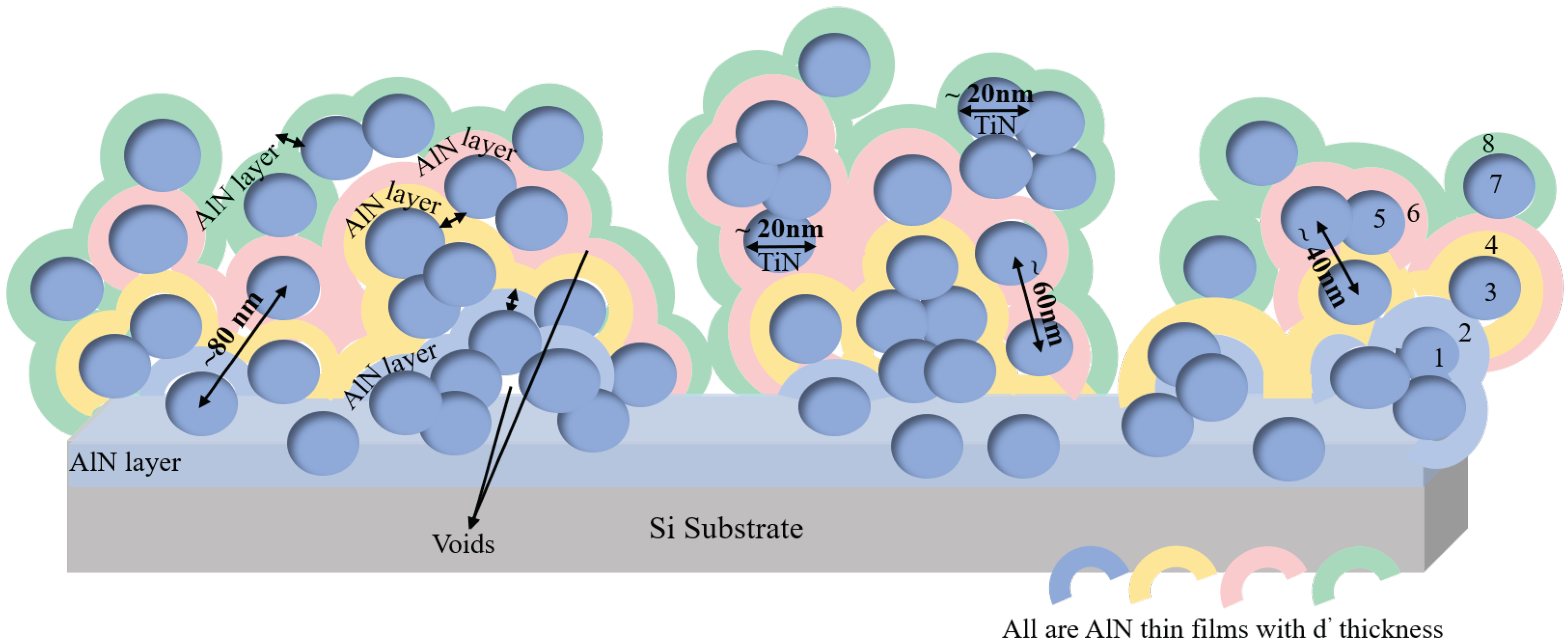
2. Structure of the Composite

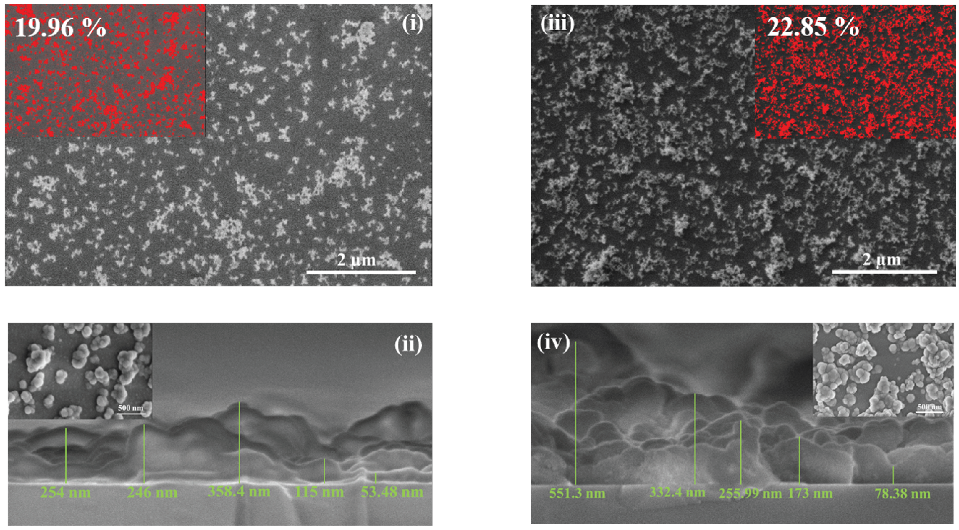
2.1. SEM Characterization

To synthesize the AlN / TiN thin-film coating, a layer-by-layer process was employed. This involved a wet-deposition technique to distribute TiN nanoparticles, followed by an atomic layer deposition ( ALD ) technique for AlN layers, as sketched in Figure 1. The simultaneous formation of both phases at the same time could not be achieved in a controlled manner (Khanna et al. [6]). Instead, the DC magnetron sputtering method proposed by Bilokur et al. [7], Du et al. [8] has enabled the deposition of titanium aluminium nitride ( TiAlN ) crystals. In contrast, our work aims to combine the distinct properties of TiN and AlN within a single composite. The composite was formed by depositing multiple layers of TiN nanoparticles embedded in an AlN matrix, stacked on top of each other, resulting in a total thickness of a few hundred nanometres. Each layer was created by first dispersing TiN nanoparticles onto the previous layer using a liquid suspension, followed by embedding them in the AlN matrix. A conformal deposition of AlN onto the TiN NP dispersion is performed. The synthesis process is detailed in Khanna [9]. Figure 1 shows a schematic of the composite, showing details of deposition in cross-sectional views. The layer’s number, from 1 to 8, is indicated on the right-hand side of the image, where odd numbers correspond to TiN deposition cycles, and even numbers correspond to alternating AlN layer depositions. Two specimens of the TiN NP suspension were considered. The first specimen was made from dry powder of TiN , while the second specimen was a ready-to-use suspension. The development of the composite was guided by a material design approach based on numerical simulations. These simulations indicate that the composite’s optical properties can be adjusted by manipulating the distribution of TiN particles embedded within the AlN matrix, enabling the prediction of an optimal configuration. In this paper, composite I will be regarded as the one prepared with dry powders of TiN , while composite II is the one prepared with the ready-made TiN suspensions. Figure 2i,iii show the top view of the very first layer of composites I and II, respectively, and (ii) and (iv) are the cross-sectional view of the synthesized layers of composites I and II, respectively. During SEM analysis, the surface coverage was estimated to be approximately 20 % for composite I and 23 % for composite II. Additionally, it was observed that the average thickness of the composites varied. This is possibly due to the presence of a large amount of agglomerations of NPs, both the dry powder and ready-made dispersion, leading to chunks of a few nanometres accumulating, one on top of the other.
In addition, manual control over the TiN NPs’ distribution throughout the composite leads to an inhomogeneous distribution in some places, making agglomerates of NPs, as represented in Figure 1. Overall, it was observed that the average thickness was smaller for composite I. This was verified by measuring the thickness at various positions on the sample. A key reason for this behaviour could be the addition of dispersant in the ready-made TiN suspensions. This is clearly seen in Figure 2, where TiN NPs cover more area in the case of composite II than in composite I (colour threshold for NP area calculation is shown in red). Thickness differences between the two composites were also confirmed by SE. This is explained in detail later, in Section 4.2. It is also evident from Figure 2ii,iv that the two types of composite possess a high degree of roughness due to the agglomeration of the NPs.

2.2. XPS Characterization

XPS analysis was performed using a Kratos Axis Ultra DLD instrument with an Al (1486.6 eV) X-ray source and a 4 keV argon ion gun for etching. This setup enables the determination of the in-depth elemental composition and distribution of the primary constituents. XPS analysis confirms the presence of TiN , AlN , and Al 2 O 3 in the core of the composite. The formation of Al 2 O 3 was attributed to oxidation during the composite preparation process. This occurred due to air exposure after each AlN thin-film deposition and the post-deposition oxygen plasma treatment of AlN , intended to enhance the adhesion of TiN nanoparticles. The upper surface, which is strongly oxidised due to the direct contact with atmospheric oxygen, was a mixture of AlN and Al 2 O 3 . The surface of AlN films is prone to oxidation, and the emergence of different forms of oxides and hydroxides on its surface has been previously reported (Liao et al. [10], Méndez et al. [11], Jose et al. [12], Zhang [13]). Al 2 O 3 and AlON are optically transparent materials over the light spectrum, near-ultraviolet, visible, and midwave-infrared regions; therefore, their presence would not have any negative impact on the optical properties of the composites. Notably, the Si signal and the oxygen associated with Si , which become prominent at longer etching times, were excluded from the percentage calculations to better highlight the trends of the elements of interest.
The XPS analysis results suggested that the composite could be considered as consisting of two distinct layers, with the upper one, referred to as layer 1, being composed of AlN and Al 2 O 3 , while the one below, designated as layer 2, comprised a blend of AlN , Al 2 O 3 , and TiN . Cross-sectional SEM images confirmed that the thickness varied between samples of composites I and II, leading us to approximate an effective thickness for each of the two layers. Table 1 gives the chemical composition at different times of etching starting from the top surface of the composite until the Si substrate is reached. Information from 0 s to 60 s (shown in red) about etching timing is completely ignored, due to the presence of carbon impurities, as shown in the C 1 s % column. Information from 120 s to 900 s (shown in blue) is considered as layer 1, where Ti is absent; thus, only AlN and Al 2 O 3 are present. The presence of AlN and Al 2 O 3 was investigated through high-resolution scans acquired for Al 2 p , N 1 s , O 1 s , Ti 2 p , and orbitals. For layer 2, information from 1200 s to 4200 s (shown in purple), showing the presence of Ti along with Al , N , Si , and O , is considered as the main layer of the composite. The signals from 4800 s to 6000 s (shown in yellow) correspond to the oxidation layer of the silicon wafer, and the remaining data from 6600 s to 9000 s correspond to the silicon wafer substrate. We estimated the thickness of layer 1 t 1 and the thickness of layer 2 t 2 as
t 1 = 1050 s 120 s 4200 s 120 s × L 68 nm t 2 = 4200 s 1050 s 4200 s 120 s × L 232 nm
t 2 = 4200 s 1050 s 4200 s 120 s × L 232 nm t 2 = 4200 s 1050 s 4200 s 120 s × L 232 nm
Here, L = 300 nm represents the average thickness of the composite, while 4200 s corresponds to the etching time just before the Si signal reaches its peak. The etching begins penetrating layer 1 at 120 s . The etching time 1050 s is considered the transition between layers 1 and 2, as it lies halfway between 900 s and 1200 s . These thicknesses would provide a useful reference for subsequent FEM simulation and SEM calculations. The volume fractions of corresponding phases in layer 1 and layer 2 were estimated as outlined in the equations below. For layer 1, the average percentage composition is 44.76 % for Al 2 p , 28.56 % for N 1 s , and 26.67 % for O 1 s . Assuming that the 28 atoms of N are bonded to 28 atoms of Al to form 28 molecules of AlN , this leaves 16 out of 44 atoms of Al available to bond with 26 atoms of O . For Al 2 O 3 , 8 atoms of Al combine with 24 atoms of O . While there are 26 oxygen atoms in total, the remaining 2 are disregarded for simplicity, as the calculations are only approximations.
v AlN = atomic mass of AlN density of AlN = 13.4 cm 3 v Al 2 O 3 = atomic mass of Al 2 O 3 density of Al 2 O 3 = 25.7 cm 3
v Al 2 O 3 = atomic mass of Al 2 O 3 density of Al 2 O 3 = 25.7 cm 3 v Al 2 O 3 = atomic mass of Al 2 O 3 density of Al 2 O 3 = 25.7 cm 3
where v AlN represents the molar volume of AlN , and v Al 2 O 3 represents the molar volume of Al 2 O 3 . The total volume of AlN is determined as V AlN = 28 × 13.4 cm 3 = 375.2 cm 3 , while the total volume of Al 2 O 3 is calculated as V Al 2 O 3 = 8 × 25.7 cm 3 = 206.1 cm 3 . Thus, the volume fractions in layer 1 are deduced as follows:
v f AlN = V AlN V AlN + V Al 2 O 3 = 0.64
and
v f Al 2 O 3 = V Al 2 O 3 V AlN + V Al 2 O 3 = 0.35
With same reasoning for layer 2, the average percentage composition is 35 % for Al 2 p , 17.44 % for N 1 s , 38.54 % for O 1 s , and 8.10 % for Ti 2 p . Assuming that 8 atoms of N bond to 8 atoms of Ti to form 8 molecules of TiN , this leaves 9 out of 17 atoms of N to bond with 9 atoms of Al , resulting in 9 molecules of AlN . The 26 atoms of Al left over bond to 13 atoms of O , forming 13 molecules of Al 2 O 3 . As the molar volume of TiN is
v TiN = atomic mass of TiN density of TiN = 11.4 cm 3
we deduce that V AlN = 9 × 13.4 cm 3 = 120.6 cm 3 ; that for Al 2 O 3 is V Al 2 O 3 = 13 × 25.7 cm 3 = 334.1 cm 3 ; and that for TiN is V TiN = 8 × 11.4 cm 3 = 91.2 cm 3 . Thus, the volume fractions of the phases in layer 2 are
v f AlN = V AlN V AlN + V Al 2 O 3 + V TiN = 0.22 , v f Al 2 O 3 = V Al 2 O 3 V AlN + V Al 2 O 3 + V TiN = 0.61 a n d v f TiN = V TiN V AlN + V Al 2 O 3 + V TiN = 0.16
,
v f Al 2 O 3 = V Al 2 O 3 V AlN + V Al 2 O 3 + V TiN = 0.61 , v f Al 2 O 3 = V Al 2 O 3 V AlN + V Al 2 O 3 + V TiN = 0.61 a n d v f TiN = V TiN V AlN + V Al 2 O 3 + V TiN = 0.16
and
v f TiN = V AlN V AlN + V Al 2 O 3 + V TiN = 0.16 , v f Al 2 O 3 = V Al 2 O 3 V AlN + V Al 2 O 3 + V TiN = 0.61 a n d v f TiN = V TiN V AlN + V Al 2 O 3 + V TiN = 0.16

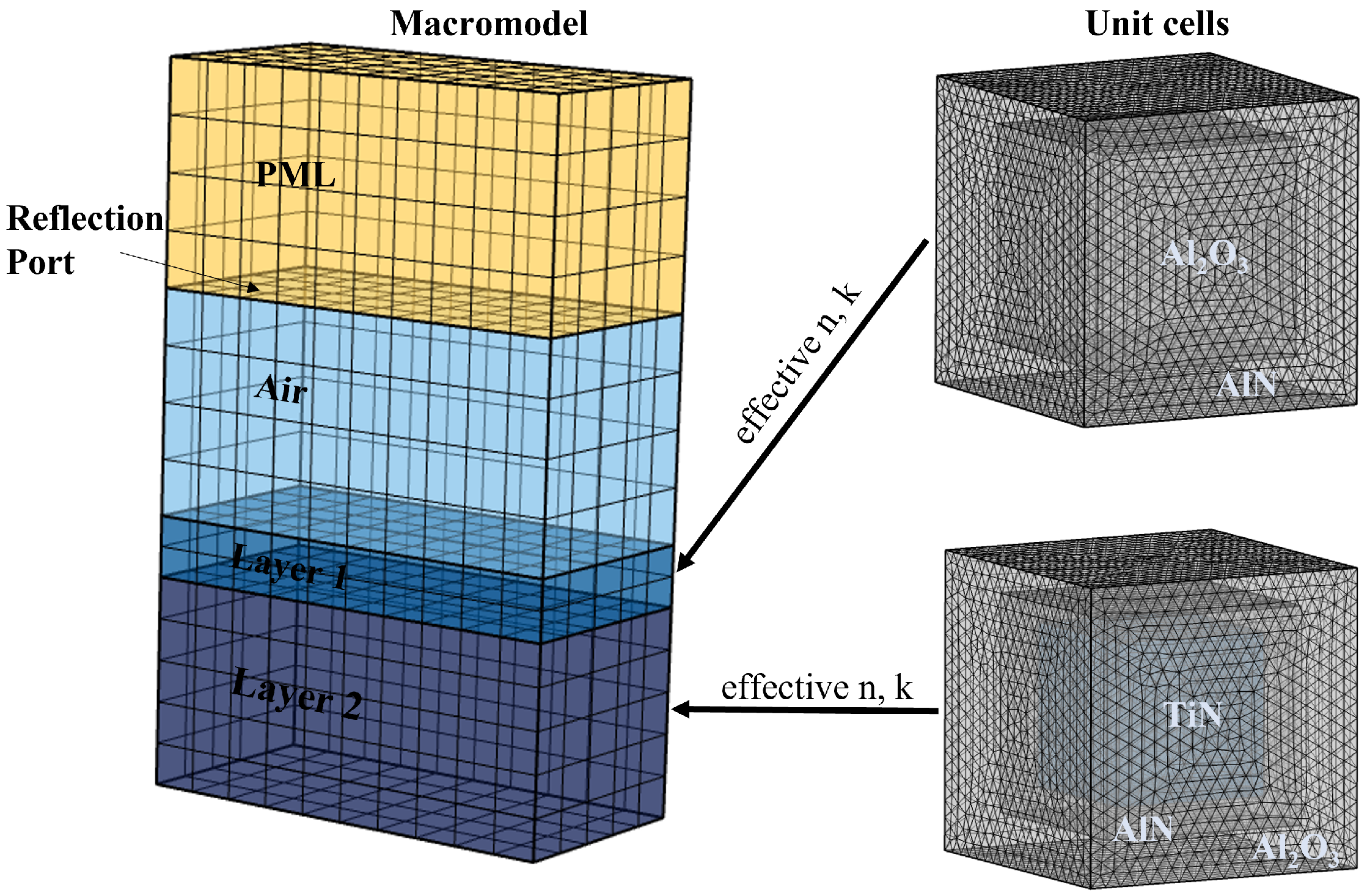
3. Numerical Modelling

Typical solar absorbing materials used for solar–thermal conversion are often conceived as a composite dielectric of metal cermets. Metal nitrides have been investigated for their potential advantages, such as weather resistance, high melting points, and enhanced optical and electrical properties (Khanna et al. [6], Rohmer et al. [14], Chang et al. [15], Nelson and Wagner [16]). In the past decade, the multidisciplinary element in materials science research has raised the degree of complexity in the systems under study (Dobrzański [17], Siegenfeld and Bar-Yam [18]). The use of powerful numerical modelling tools has provided exceptionally accurate predictions of the physical processes and suggested numerous advanced possibilities for optimized experimental procedures (Körkel et al. [19], Tan et al. [20]).
To simulate the interaction between light and the composite dielectric material, and subsequently the wave optics interaction with nanoparticles, we solve Maxwell’s Equation (11) in the frequency domain for wave propagation through the composite film in a steady state.
× × E k 0 2 n ˜ 2 E = 0
Here, E represents the electric field vector and k 0 denotes the wave number in free space. It is also essential to qualitatively study the optical properties of the individual components of the composite. The dielectric loss is expressed within a complex wave vector as
k ˜ = k j k = n ˜ k 0
Here, n ˜ is the complex refractive index of the medium. Its real part n and imaginary part κ are both intrinsic values of a material that depend on the wavelength of the incident light and are related to the complex relative dielectric function, ε ˜ (Batsanov et al. [21]), as
n ˜ = n j κ = ε r ˜ ( ω )
where n is defined by Snell’s law (Bahaa E. A. Saleh [22]) as the ratio between the speed of light inside the medium, v, and the speed of light in vacuum, c =299,792,458 m/s:
n = c v
Meanwhile, κ is the wave extinction. It is related to absorption and represents dielectric loss, due to the delayed response of molecular dipoles, Joule losses from conduction, and wave scattering extinction. The attenuation of light intensity I, as the light travels through the medium, is described by the Beer–Lambert law (Mayerhöfer et al. [23]):
I ( d ) = I 0 e a d
where (a) is the attenuation coefficient and (d) is the distance travelled by the wave inside the material. The value of (a) is related to the extinction coefficient κ of the material according to
a = 4 π κ λ
It follows that
l n ( I I 0 ) = a d = 4 π κ d λ
If the film is such that λ κ d , then it becomes transparent (Zhang et al. [24], Pérez [25], Chen and Boström [26]). Reflection occurs at the interface between two media with differing refractive indices. As light propagates through a medium, some of it is absorbed. Consequently, transmittance represents the fraction of the light beam that successfully passes through the medium, such that
R + T + A = 1
In order to design a good solar light absorber with spectral selectivity, we choose materials that lead to an effective refractive index, close to that of air in the visible part of the spectrum to minimize reflection, while being higher in the infrared region to maximise reflection and reduce blackbody radiation loss. Figure 3 presents the refractive index curves of the material phases. The AlN and Al 2 O 3 curves exhibit no dispersion across the visible to infrared spectrum, meaning that refractive index remains constant, and there is zero extinction coefficient. This transparency makes these materials highly efficient for light transmission. In contrast, TiN is conductive, exhibits high loss, and is dispersive, with a refractive index near unity in the visible spectrum but increasing significantly in the infrared region. When designing the composite dielectric TiN / AlN - Al 2 O 3 , care is taken to prevent TiN nanoparticles from reaching the percolation threshold by avoiding agglomeration that could cause excessive reflection in the visible region and considering smaller particles to enhance scattering extinction (Striebel et al. [27]).

3.1. Numerical Acquisition of
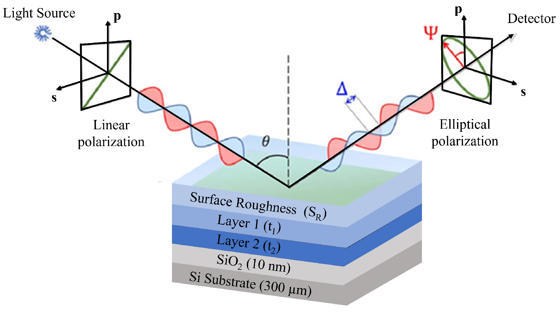
 n ˜ ( λ )

The homogenization theory was introduced by Maxwell Garnett [28]. Since then, many empirical formulations have been derived using the Maxwell Garnett and Bruggeman approximations to calculate the effective dielectric constant for composites with various shapes and types of inclusions (Doyle [29], Markel [30]). Recently, however, finite-element-based methods have become the most preferred due to their simplicity (Nayak et al. [31]). Here, for the estimation of the effective optical parameters of the composite, we solve the problem of wave propagation at normal incidence, through an infinitely long dielectric slab, as sketched in Figure 4, in the frequency domain using the finite element method and calculate the scattering matrix S i j . Then, the values of n and κ are derived using the algorithm described below. To achieve this, we assume a symmetric medium in which S i j = S 11 , S 21 .
Figure 4 shows the field components, propagating from left side to right side through the dielectric film. Here, the subscripts and r denote left and right, respectively, while the superscripts i , s , and t denote incident, scattered, and transmitted components, respectively. Inside the dielectric, forward-propagating components are denoted by the superscript +, while backward-propagating components are denoted by the superscript −. The elementary reflection coefficients at the left and right sides are denoted by ρ and ρ r , respectively. Assuming the presence of air on both sides of the dielectric, i.e., n = n r = n 0 , then
ρ = ρ r = n 0 n ˜ d n 0 + n ˜ d
The relationships between the field components across the interfaces are given in Orfanidis [32] and are expressed in a straightforward way using the matching matrices
E i E s = 1 ρ + 1 1 ρ ρ 1 E + E
E r + E r - = 1 ρ r + 1 1 ρ r ρ r 1 E r t 0
and the propagation matrix
E + E = e j k ˜ d 0 0 e j k ˜ d E r + E r
The relationships
E i = 1 ( ρ + 1 ) ( ρ + 1 ) e j k ˜ d + ρ ρ r e j k ˜ d E r t
and
E s = 1 ( ρ + 1 ) ( ρ + 1 ) ρ e j k ˜ d + ρ r e j k ˜ d E r t
lead to the expressions
S 11 = E r E i = ρ + ρ r e j 2 k ˜ d 1 + ρ r ρ e j 2 k ˜ d
and
S 21 = E r t E i = 1 + ρ 1 + ρ r e j k ˜ d 1 + ρ r ρ e j 2 k ˜ d
for the scattering parameters. In the simulations at nanoscale, we consider the same medium on the left and right sides; therefore, we set
e j k ˜ d = Γ = Γ e + j ϕ ρ = ρ r = ρ
and we obtain the values
ζ + ζ 2 1 = ρ ζ = S 11 2 S 21 2 + 1 2 S 11
and
Γ = ρ S 11 S 21 ρ ( S 11 + S 21 ) 1
The values of S 11 and S 21 in Equation (29) are determined from simulation on the unit cell, representing the dielectric composition at the nanoscale, as described in Section 4.1 below. Finally, the complex refractive index of the slab (Nicolson and Ross [33], Smith et al. [34]) may be determined as
n d ˜ = 2 π m ϕ k 0 d + j ln Γ k 0 d
Here, the coefficient m denotes the branch order of the inverse tangent function.

3.2. Acquisition of n ˜ ( λ ) from SE Measurements

SE is primarily a technique for measuring the optical properties of thin coating materials with polarized light. The measurements are based on the analysis of the polarization of the light beam reflected from the sample surface. Figure 5 shows a schematic representation of the SE measurement. A linearly polarized light beam illuminates the sample with a specified incidence angle. Upon reflection, the beam transforms into elliptically polarized light (Lissberger [35]), with the polarization change being entirely dependent on the wavelength, the angle of incidence, the thickness of the layers in the sample, and, most importantly, their optical model. The changes in polarization are expressed through ellipsometric parameters, namely the phase difference △, which represents the difference between the s-wave and p-wave components of the reflected wave, and tan Ψ , which relates to the amplitude change. The angle of incidence for the interaction between the beam and the sample should be close to Brewster’s angle, where this method is most effective (Bakker et al. [36]). A model is chosen to represent the sample’s characteristics, and the parameters △ and Ψ are compared to the measured values. This model applies mathematical dispersion formulas to determine material properties, such as thickness, surface roughness, and optical parameters, by adjusting specific fitting parameters. The constructed model describes the individual layers in terms of their thicknesses and optical parameter values (Yusoh et al. [37]).
R p R s = E p r / E p i E s r / E s i = tan Ψ . e j
where R p and R s denote the reflection coefficients of the p-polarized and s-polarized light, respectively. E p i , r denotes the intensities of the incident and reflected electric field of the p-wave and E s i , r denotes the intensities of the incident and reflected electric field of the s-wave.

4. Results and Discussion

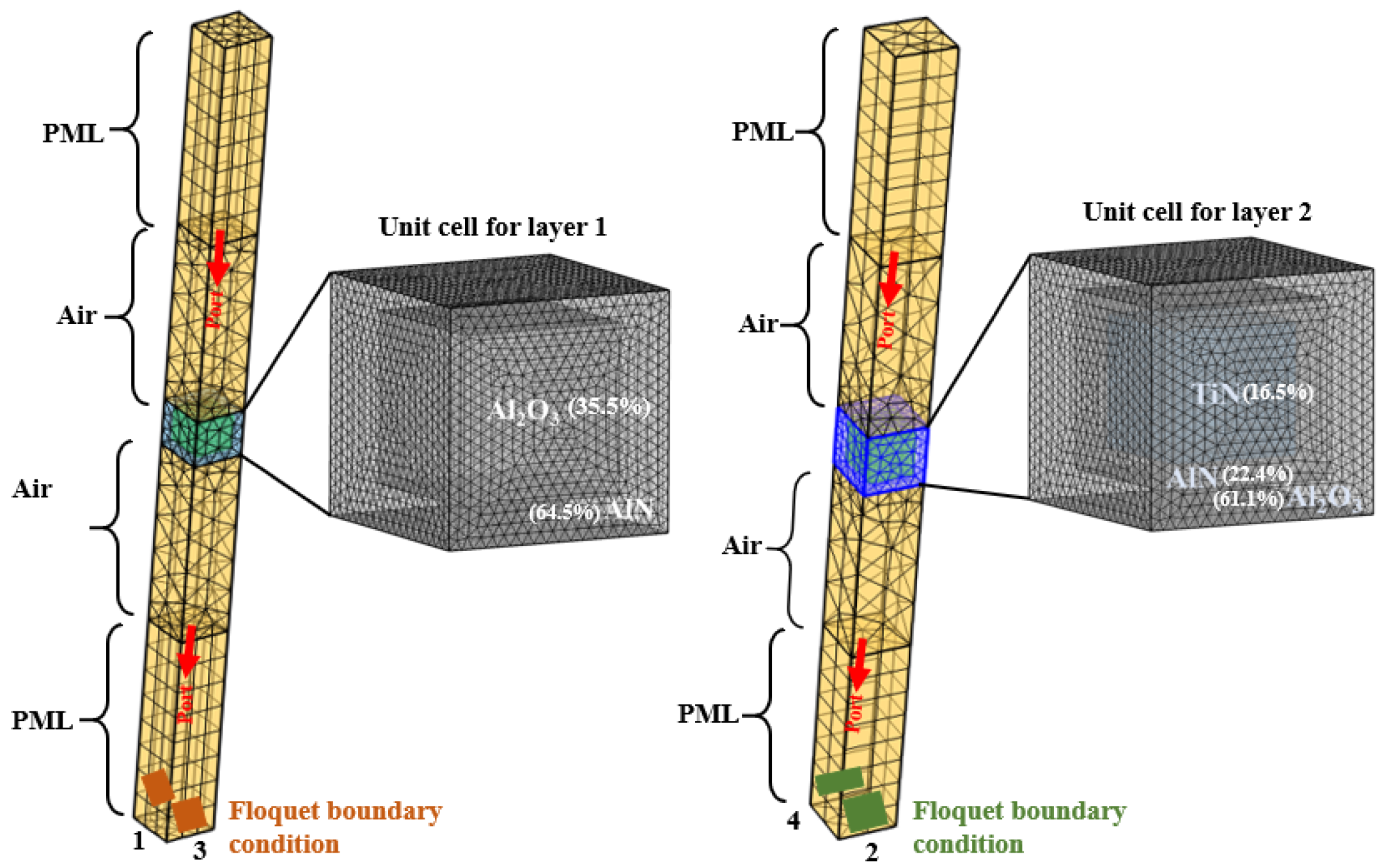
4.1. Numerical Simulation

Considering the volume fractions shown in the XPS table (Table 1), a unit cell model was created for layers 1 and 2 in order to calculate the effective parameters n and κ as shown in Figure 6. The left side shows details of the whole computational domain of the nanoscale model, with the Al 2 O 3 phase embedded in an AlN matrix forming a representative unit cell for layer 1. On the right side of the figure, it shows TiN and AlN embedded in an Al 2 O 3 matrix forming a representative unit cell for layer 2.
Equation (11) is solved within the nanoscale model with the following boundary conditions:
  • Perfectly Matched Layers (PMLs) were applied to the top and bottom domains of the computational domain to simulate an infinite space. Both the PMLs and air regions were assigned a thickness equal to ( λ / 2 ) each.
  • The boundary surfaces between the PML domain and the air spacing serve as ports for initiating the incident wave illumination and for post-process calculation of the scattering coefficients S i j .
  • Floquet periodic boundary conditions are implemented on the transverse sides of the computational domain to emulate an infinitely extensive film.
The TiN phase has a width of 20 nm and the unit cell has a width of 26 nm . These sizes are determined to comply with the volume fraction of the phases. The maximum mesh element size allowed here in the nanoscale model simulation is λ / 15 . The calculation takes 15 min to complete the frequency sweep over the VIS-IR range. The S-parameters are post-processed for the representative unit cell, and then the optical properties are retrieved, as explained in Section 3.1. The results from these numerical models are compared to those obtained experimentally from SE in the following sections.

4.2. Optical Measurements by Spectroscopic Ellipsometer

The numerical model for retrieving optical properties is validated by performing measurements on the synthesised samples. Due to the wide susceptibility in ellipsometry, employing a dependable and efficient numerical approach to forecast outcomes before conducting experiments is highly advantageous. This is especially useful for analysing systems with intricate nanostructures. Here, we introduce a straightforward method, offering thorough SE analysis for complex multi-layer systems. This approach allows flexibility in design regarding thickness, the number of layers, and phase composition. The SE analysis was conducted over the spectral range ( 370 nm to 1600 nm ) allowed by the apparatus bulb. A standard model was developed to analyse composites I and II, reflecting the characteristics of the real samples. The model was initiated with a 300 μ m thick Si wafer and a thin 10 nm oxidised layer of SiO 2 on top. For layer 2, a Cauchy model was created for the conductive TiN embedded within a insulating matrix of mixed AlN and Al 2 O 3 ; thus, the Cauchy absorbent dispersion law was applied. This approach is typically used to describe the optical properties of materials that are weakly absorbent. Since the TiN content in the composite is only 20 % , it qualifies as weakly absorbent. The Cauchy absorbent model is defined as
n ( λ ) = A + 10 4 λ 2 B + 10 9 λ 4 C
k ( λ ) = 10 5 · D + 10 4 λ 2 E + 10 9 λ 4 F
Six fitting parameters are employed in this model, where the first three—A (dimensionless), B ( nm 2 ), and C ( nm 4 )—have to fulfil the condition
0 < C < B < 1 < A
The extinction coefficient is described by the other three fit parameters: D (dimensionless), E ( nm 2 ), and F ( nm 4 ). Layer 1 was modelled using the ‘Cauchy Transparent’ model. This layer comprises only a transparent mixture of AlN and Al 2 O 3 . This implies that κ ( λ ) = 0 .
n ( λ ) = A + 10 4 λ 2 B + 10 9 λ 4 C
κ ( λ ) = 0
This model is most effective for materials with no optical absorption in the visible spectral range, typically exhibiting normal dispersion, where n decreases as the wavelength increases. Surface roughness was a significant factor in our case, as both composites demonstrated substantial roughness. Consequently, an additional layer representing the real surface roughness, modelled with a gradient, was added on top of the model. To construct the Cauchy model for both layers, the thicknesses t 1 and t 2 were initially fixed at 68 nm and 232 nm , respectively (as determined in Section 2.2). This approach allowed us to calculate the values for A, B, C, D, E, and F for both layers. Once the values of these six parameters were established, a standard model was generated. During the analysis of four samples for each composite (I and II), the thicknesses t 1 and t 2 and the surface roughness were adjusted for fitting in each iteration.
Table 2 presents the fitting parameters of the Cauchy model used to retrieve the optical functions from SE measurements. The thicknesses t 1 and t 2 and surface roughness S R obtained for different samples are listed in the top lines. The bottom lines list the Cauchy parameter values for corresponding layers 1 and 2 of each sample. The consistent parameter values across all samples demonstrate excellent reproducibility, validating the reliability of the synthesis technique employed. The layer thicknesses align closely with averages obtained from SEM images and those derived from XPS data, reinforcing the observation that the average coating thickness, L, is greater for composite II. These results further support the predictions of the numerical model for such a complex nanostructure.

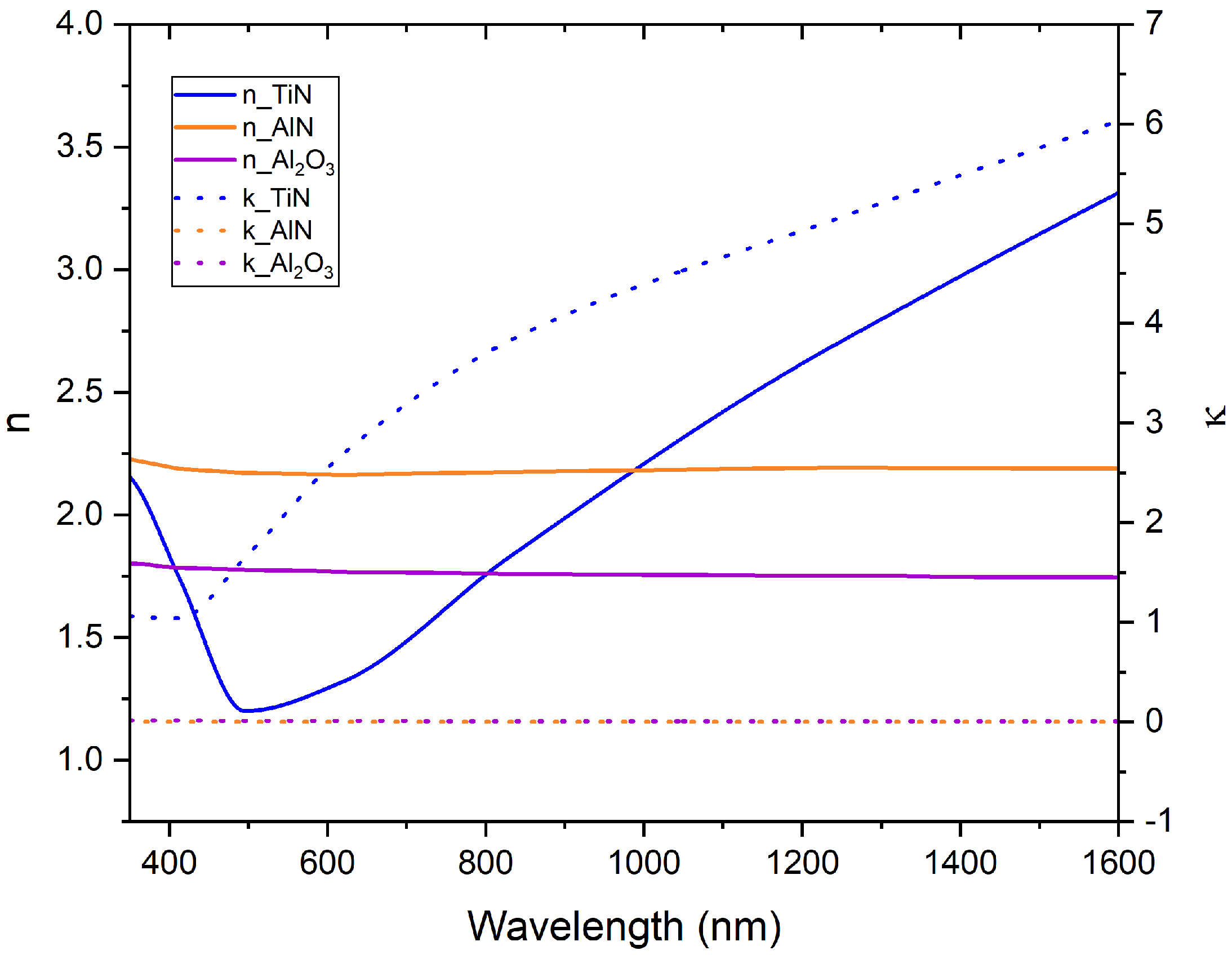
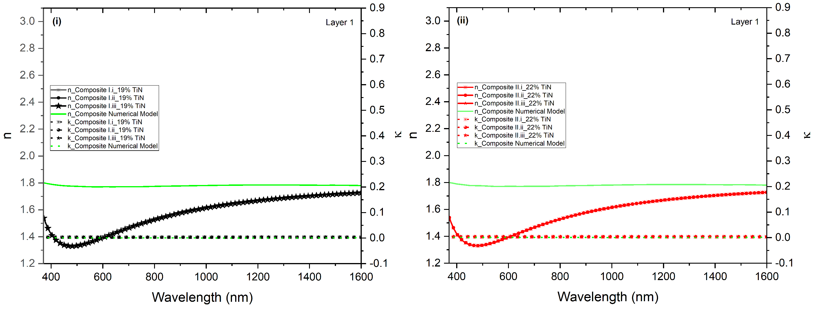
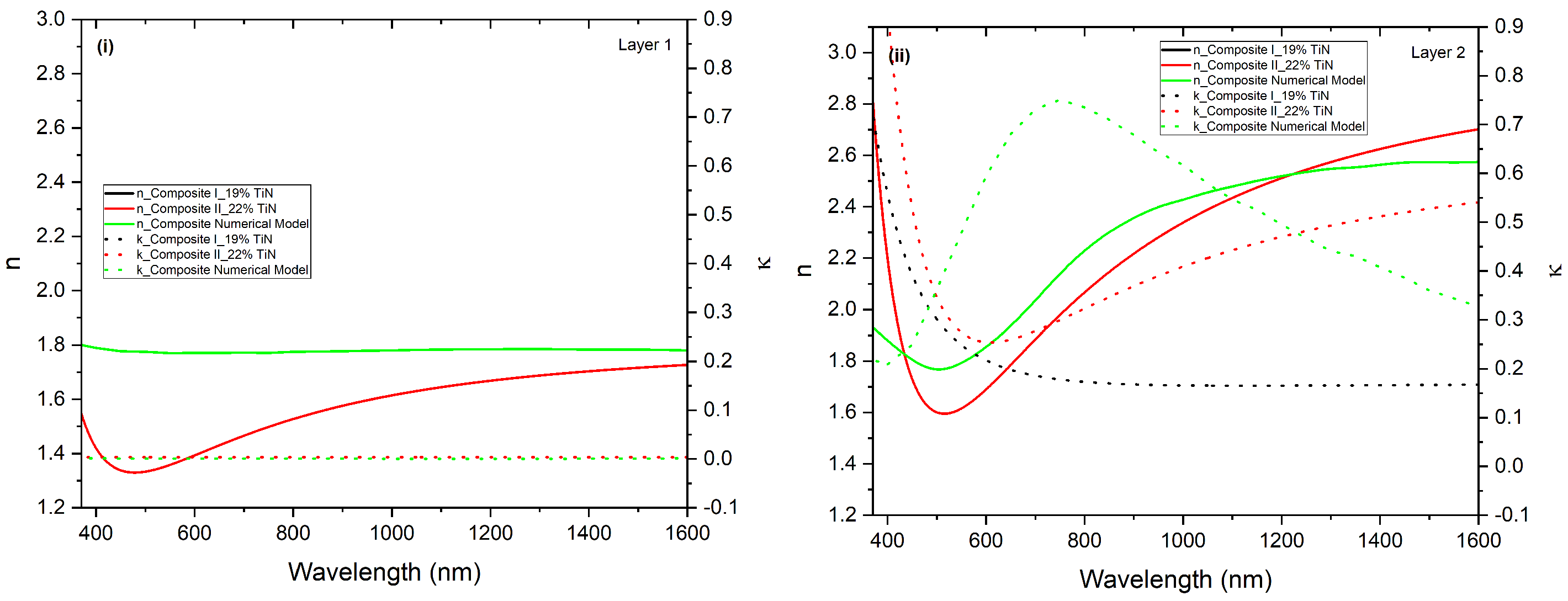
4.3. Analysis of the Retrieved Refractive Index for Composites I and II

The above discussion provides a foundation for the methodology used to determine n and κ for the complex composite structure. To enhance understanding and improve accuracy in assessing the performance of the two composites regarding their light absorptance and reflectance, obtaining refractive indexes for both layer 1 and layer 2 of composites I and II is essential. This section presents a clear comparison, emphasizing differences and offering logical explanations behind the experimentally and numerically obtained optical properties. The values of n and κ from numerical simulations were derived at an incident angle of 50 .
In Section 4.1, the volume fractions used for numerical calculations were derived from XPS data shown in Table 1. The surface roughness was not incorporated within the initial model. The wave optics module in COMSOL Multiphysics software does not include a feature to directly account for roughness, yet our samples exhibit a significant degree of roughness, making it necessary to consider this factor when calculating n and κ . To address this, we included an air fraction of 25 % to the unit cell of layer 1 as an alternative way to model the roughness.
Surface roughness values, approximately 60 nm as shown in Table 2, are smaller than the wavelengths in the studied spectrum ( 370 nm to 1600 nm ), justifying the homogenization approach. This assumes that the voids contributing to roughness are part of a smooth layer 1 comprising AlN and Al 2 O 3 phases. Figure 7 compares the refractive index and extinction coefficient values of layer 1 for three samples with subscripts (_i, _ii, _iii) of both composites and the numerical model predictions. The solid curves represent the refractive index n, while the dashed curves depict the extinction coefficient κ . Green curves illustrate the numerical predictions for the upper layer 1, black curves in Figure 7i correspond to composite I, and red curves in Figure 7ii correspond to composite II.
The nanoscale simulations assume a uniform mixture of Al 2 O 3 , AlN , and air in layer 1, leading to a quasi-constant n and a negligible κ over the spectrum, as seen in Figure 7. This prediction aligns consistently across the spectral range. The calculated n and κ values for the AlN , Al 2 O 3 , and air mix are well justified and align with the XPS analysis results presented in Table 1 during the initial etching phase until the composite core is reached. As a combination of three dielectric materials, the experimental κ values for layer 1 in all samples of both composites remain nearly zero, rendering layer 1 completely transparent. Notably, the n and κ values for layer 1 across all samples are identical, resulting in overlapping curves.
Figure 8 illustrates the comparison of optical functions for each sample of both composites I and II, alongside numerical predictions for layer 2. On the left (i), the n values for samples (_i) and (_ii) closely align, while sample (iii) shows a slightly lower n in the visible region of the spectrum. The κ values for the samples of composite I range from 0.1 to 0.35 and show good agreement across the spectrum. However, the κ values obtained from the nanoscale model, represented by the dashed green curve, present high values in the visible range. This discrepancy arises because the numerical model assumes an idealized scenario with a perfect, periodic distribution of TiN inclusions within the AlN and Al 2 O 3 matrix, which explains the resulting destructive interference.
All curves representing n converge in the infrared (IR) region, following a similar trend with moderate differences. Variations among the samples are attributed to the imperfect distribution of TiN NPs within the matrix. Since the TiN NPs were laid randomly in a wet solution, some inhomogeneity occurred, leading to the formation of agglomerates and clusters in specific areas, which altered light interaction behaviour. The higher κ values observed in Figure 8ii are due to a greater concentration of TiN particles in composite II. This is supported by SEM images in Figure 2, which show a TiN inclusion distribution of 22 % in composite II compared to 19 % in composite I.
The electrically conducting nature of TiN nanoparticles in the layer 2 of the composite makes its κ values significantly elevated in both composites compared to the ones of layer 1. Figure 9i,ii provide a comparison of functions n and κ for composites I and II, covering, respectively, layer 1 and layer 2 alongside the numerical predictions. Figure 9i highlights the n and κ values for layer 1, showing that the refractive index values for both composites are lower than the numerical predictions in the visible range. This discrepancy is likely due to inaccuracies in the fitting model in the SE software (completeEASE M2000), while the dip seen at 500 nm is due to the TiN refractive index, as illustrated in Figure 3. Figure 9i compares the n and κ values of layer 2 for composites I and II with the nanoscale predictions. Although the distribution of TiN nanoparticles was manually controlled, it can be observed that the constant optical values for the three samples of each composite and the numerical predictions were consistent and within a comparable range.

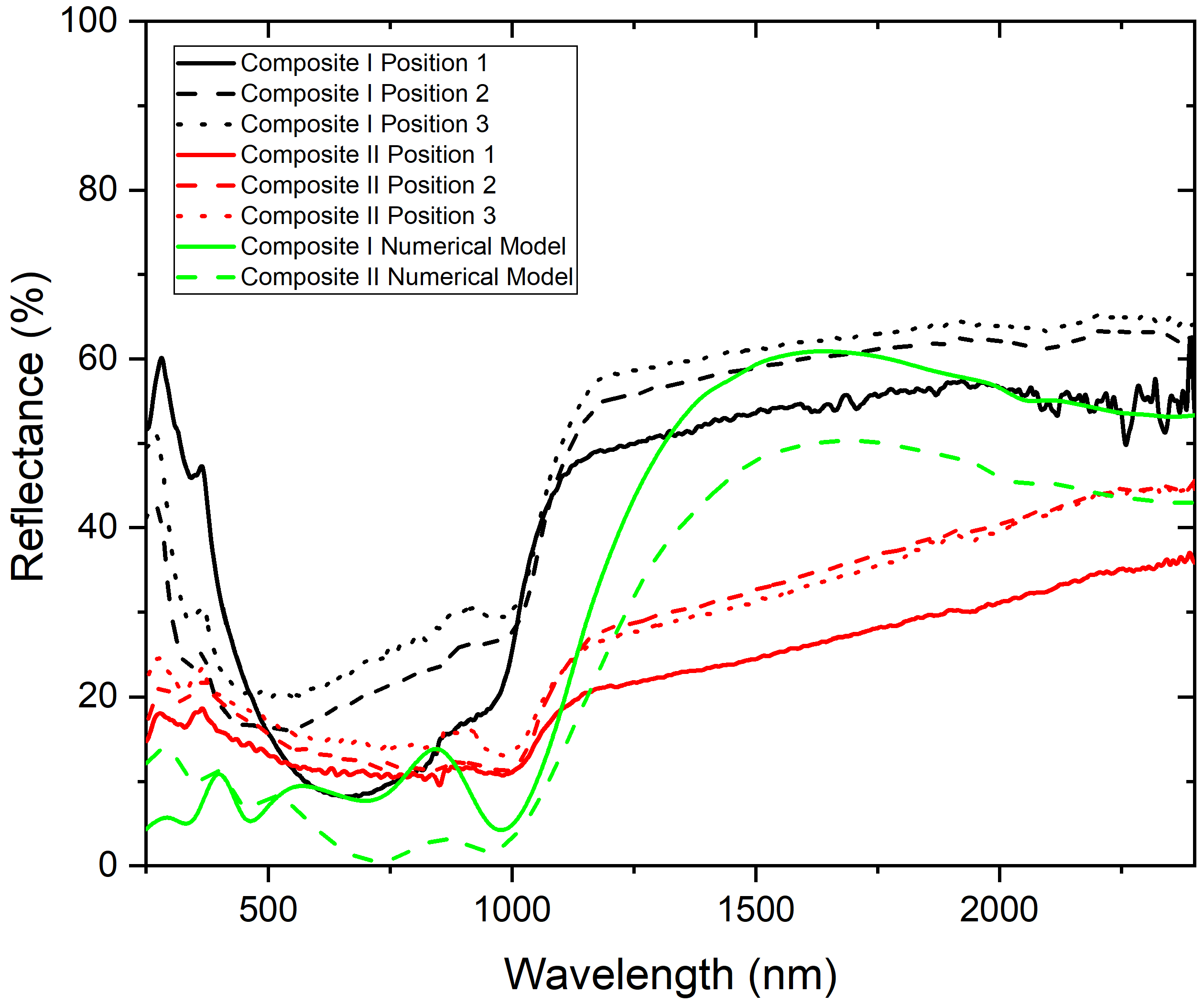
4.4. Analysis of the Reflectance Properties of Composites I and II

To validate the numerical characterization approach of the nanostructured composite, measurements of the reflectance of composites I and II were performed using a UV–visible spectrophotometer based on parameters such as the size of the TiN nanoparticles and the volume fraction of TiN within the AlN matrix. A spectrally selective filter was designed to achieve minimum reflection in the visible region and maximum reflectance in the IR region of the spectrum. The effective optical parameters of the composite, including the refractive index (n) and extinction coefficient ( κ ), were retrieved for both composites I and II.
The macromodel, simulating the homogeneous layers of the composite as shown in Figure 10, was refined based on the outcomes of the XPS characterization. These refinements specifically addressed the presence of a certain fraction of alumina ( Al 2 O 3 ) and the thicknesses of the layers (see XPS results in Table 1). The effective optical parameters derived from the nanoscale model were incorporated into the homogenized macromodel to evaluate the reflectance across the visible light spectrum. Since the size of the TiN NPs is extremely small compared to the wavelength, the shape effect of the NPs is negligible; therefore, the NPs were modelled as cubes in the unit cells of the nanoscale model. The side of the TiN cube was set to 20 nm, while the unit cell width was determined as 26 nm based on the volume fraction of the phases.
The composite was divided into two layers, layer 1 and layer 2, for the macromodel simulations. The n and κ values retrieved from the unit cell prepared with an AlN matrix containing a volume fraction of Al 2 O 3 and air, with the corresponding thickness deduced from XPS data, were assigned to layer 1. Similarly, the n and κ values from the unit cell prepared with an Al 2 O 3 matrix containing volume fractions of AlN and TiN , with the corresponding thickness deduced from XPS data, were assigned to layer 2.
The measurements of reflectance in the VIS-IR range were performed using a Perkin Elmer Lambda 750 spectrophotometer. Figure 11 compares the measured and computed reflectance for both composites. The curves shown in black colour represent measurements performed at three different locations on composite I wafer, while the curves in red colour correspond to three different locations on the composite II wafer. Both groups of curves are closely aligned, with a reflectance difference of approximately 10 % across the entire spectral range. The variation between black and red group of curves is attributed to differences in the TiN content within composites.
The black curves show a higher reflectance in the IR region. This is primarily due to two factors: first, composite II contains more TiN and larger agglomerates compared to composite I; second, composite I has a lower AlN content (and therefore a higher refractive index, n) than composite II. The dotted green curve in the figure corresponds to predicted reflectance from the macromodel simulation for composite II, while the solid green curve corresponds to predicted reflectance from the macromodel simulation for composite I.
The predicted reflectance curve in solid green matches the measured reflectance for composite I because composite I is more homogeneous and exhibits smaller agglomerates of the TiN NPs. In contrast, the red reflectance curves differ significantly from the numerical model for composite II. This discrepancy arises because the numerical model assumes a uniformly separated distribution of TiN nanoparticles within layer 2, which was not achievable by the synthesis technique. Additionally, the nanoscale model assumes smooth surfaces, whereas the actual composites have very rough surfaces. An important observation is that the black curves exhibit a distinct filter characteristics at an infrared limit of 1 μ m .

5. Conclusions

In this study, we investigated two methods for retrieving (n) and ( κ ): one through spectroscopic ellipsometry (SE) experimental measurements and the other via numerical simulations. These approaches provided a clear framework for making structural modifications, if required. Initially, calculations based on XPS data offered rough estimates for parameters such as ( t 1 ), ( t 2 ), (L), and ( S R ), which facilitated simplifying the complex structure by dividing it into two distinct layers. Using the elemental composition data from XPS measurements, we also estimated the volume fraction of each component in the composite. These preliminary calculations were instrumental in developing models for both experimental and numerical analysis.
We successfully created a model for measuring (n), ( κ ), ( t 1 ), ( t 2 ), and ( S R ) via SE for the complex structure of the composite. Additionally, two unit cell models were developed numerically to obtain the optical parameters. Comparative analysis revealed that all samples of composites I and II were reproducible, with their optical parameter values falling within close range of one another. Furthermore, the optical parameters obtained experimentally and numerically for both composites showed a high degree of agreement. However, minor discrepancies were observed, primarily due to differences in the experimental and numerical setup of the models.

Author Contributions

M.E.H. and N.K., methodology, validation, investigation, and writing; E.B., review, editing, supervision, and administration. All authors have read and agreed to the published version of the manuscript.

Funding

This research was funded by FNR, Luxembourg, and EPSRC, United Kingdom, under grant INTER FNR–RCUK/1611584556.

Data Availability Statement

Data are unavailable publicly but can be shared upon request.

Acknowledgments

The authors would like to thank S. Krishnamoorthy, M. Michel, O. Hassan, and R. Sevilla for their helpful discussions and guidance. We also express gratitude to LIST engineers N. Adjeroud (PE-ALD), A. El Moul (SEM), and C. Vergne (XPS) for their technical support.

Conflicts of Interest

The authors declare no conflicts of interest. The funders had no role in the design of the study; in the collection, analyses, or interpretation of data; in the writing of the manuscript; or in the decision to publish the results.

References

  1. Knöner, G.; Parkin, S.; Nieminen, T.A.; Heckenberg, N.R.; Rubinsztein-Dunlop, H. Measurement of the Index of Refraction of Single Microparticles. Phys. Rev. Lett. 2006, 97, 157402. [Google Scholar] [CrossRef]
  2. Brown, R. Absorption and Scattering of Light by Small Particles. Opt. Acta Int. J. Opt. 1984, 31, 3. [Google Scholar] [CrossRef]
  3. Bohren, C.F.; Huffman, D.R. Absorption and Scattering of Light by Small Particles; Wiley: Hoboken, NJ, USA, 1998. [Google Scholar] [CrossRef]
  4. Righini, M.; Ghenuche, P.; Cherukulappurath, S.; Myroshnychenko, V.; de Abajo, F.J.G.; Quidant, R. Nano-optical Trapping of Rayleigh Particles and Escherichia coli Bacteria with Resonant Optical Antennas. Nano Lett. 2009, 9, 3387–3391. [Google Scholar] [CrossRef]
  5. Bendix, P.M.; Oddershede, L.B. Expanding the Optical Trapping Range of Lipid Vesicles to the Nanoscale. Nano Lett. 2011, 11, 5431–5437. [Google Scholar] [CrossRef]
  6. Khanna, N.; Hachemi, M.E.; Sevilla, R.; Hassan, O.; Morgan, K.; Barborini, E.; Belouettar, S. Multi-physical modelling, design optimisation and manufacturing of a composite dielectric solar absorber. Compos. Part C Open Access 2022, 8, 100282. [Google Scholar] [CrossRef]
  7. Bilokur, M.; Gentle, A.R.; Arnold, M.D.; Cortie, M.B.; Smith, G.B. High temperature optically stable spectrally-selective Ti1xAlxN-based multilayer coating for concentrated solar thermal applications. Sol. Energy Mater. Sol. Cells 2019, 200, 109964. [Google Scholar] [CrossRef]
  8. Du, M.; Liu, X.; Hao, L.; Wang, X.; Mi, J.; Jiang, L.; Yu, Q. Microstructure and thermal stability of Al/Ti0.5Al0.5N/Ti0.25Al0.75N/AlN solar selective coating. Sol. Energy Mater. Sol. Cells 2013, 111, 49–56. [Google Scholar] [CrossRef]
  9. Khanna, N. Metamaterial Design and Elaborative Approach for Efficient Selective Solar Absorber. Ph.D. Thesis, Unilu-University of Luxembourg, Belval, Luxembourg, 2022. [Google Scholar]
  10. Liao, H.M.; Sodhi, R.N.S.; Coyle, T.W. Surface composition of AlN powders studied by x-ray photoelectron spectroscopy and bremsstrahlung-excited Auger electron spectroscopy. J. Vac. Sci. Technol. A Vac. Surfaces Film. 1993, 11, 2681–2686. [Google Scholar] [CrossRef]
  11. Méndez, M.G.; Rodríguez, S.M.; Shaji, S.; Krishnan, B.; Pérez, P.B. Structural Properties of AlN Films with Oxygen Content Deposited by Reactive Magnetron Sputtering: XRD and XPS Characterisation. Surf. Rev. Lett. 2011, 18, 23–31. [Google Scholar] [CrossRef]
  12. Jose, F.; Ramaseshan, R.; Dash, S.; Bera, S.; Tyagi, A.K.; Raj, B. Response of magnetron sputtered AlN films to controlled atmosphere annealing. J. Phys. D Appl. Phys. 2010, 43, 075304. [Google Scholar] [CrossRef]
  13. Zhang, Y. Characterization of as-received hydrophobic treated AlN powder using XPS. J. Mater. Sci. Lett. 2002, 21, 1603–1605. [Google Scholar] [CrossRef]
  14. Rohmer, M.M.; Bénard, M.; Poblet, J.M. Structure, Reactivity, and Growth Pathways of Metallocarbohedrenes M8C12 and Transition Metal/Carbon Clusters and Nanocrystals: A Challenge to Computational Chemistry. Chem. Rev. 2000, 100, 495–542. [Google Scholar] [CrossRef]
  15. Chang, Y.H.; Chiu, C.W.; Chen, Y.C.; Wu, C.C.; Tsai, C.P.; Wang, J.L.; Chiu, H.T. Syntheses of nano-sized cubic phase early transition metal carbides from metal chlorides and n-butyllithium. J. Mater. Chem. 2002, 12, 2189–2191. [Google Scholar] [CrossRef]
  16. Nelson, J.A.; Wagner, M.J. High Surface Area Mo2C and WC Prepared by Alkalide Reduction. Chem. Mater. 2002, 14, 1639–1642. [Google Scholar] [CrossRef]
  17. Dobrzański, L.A. Significance of materials science for the future development of societies. J. Mater. Process. Technol. 2006, 175, 133–148. [Google Scholar] [CrossRef]
  18. Siegenfeld, A.F.; Bar-Yam, Y. An Introduction to Complex Systems Science and Its Applications. Complexity 2020, 2020, 1–16. [Google Scholar] [CrossRef]
  19. Körkel, S.; Kostina, E.; Bock, H.G.; Schlöder, J.P. Numerical methods for optimal control problems in design of robust optimal experiments for nonlinear dynamic processes. Optim. Methods Softw. 2004, 19, 327–338. [Google Scholar] [CrossRef]
  20. Tan, G.; Lehmann, A.; Teo, Y.M.; Cai, W. Methods and Applications for Modeling and Simulation of Complex Systems; Springer Nature: Singapore, 2019. [Google Scholar]
  21. Batsanov, S.S.; Ruchkin, E.D.; Poroshina, I.A. Refractive Indices of Solids; Springer: Berlin/Heidelberg, Germany, 2016; Available online: https://www.ebook.de/de/product/26683914/stepan_s_batsanov_evgeny_d_ruchkin_inga_a_poroshina_refractive_indices_of_solids.html (accessed on 19 January 2025).
  22. Bahaa, E.A.; Saleh, M.C.T. Fundamentals of Photonics; Wiley: Hoboken, NJ, USA, 2019. [Google Scholar]
  23. Mayerhöfer, T.G.; Pahlow, S.; Popp, J. The Bouguer-Beer-Lambert Law: Shining Light on the Obscure. ChemPhysChem 2020, 21, 2029–2046. [Google Scholar] [CrossRef]
  24. Zhang, K.; Hao, L.; Du, M.; Mi, J.; Wang, J.; Meng, J. A review on thermal stability and high temperature induced ageing mechanisms of solar absorber coatings. Renew. Sustain. Energy Rev. 2017, 67, 1282–1299. [Google Scholar] [CrossRef]
  25. Pérez, I.H. Multilayer Selective Coatings for High Temperature Solar Applications; Editions Universitaires Européennes: Londonm UK, 2017; Available online: https://www.ebook.de/de/product/29245585/irene_heras_perez_multilayer_selective_coatings_for_high_temperature_solar_applications.html (accessed on 19 January 2025).
  26. Chen, Z.; Boström, T. Electrophoretically deposited carbon nanotube spectrally selective solar absorbers. Sol. Energy Mater. Sol. Cells 2016, 144, 678–683. [Google Scholar] [CrossRef]
  27. Striebel, M.; Wrachtrup, J.; Gerhardt, I. Absorption and Extinction Cross Sections and Photon Streamlines in the Optical Near-field. Sci. Rep. 2017, 7, 15420. [Google Scholar] [CrossRef] [PubMed]
  28. Garnett, J.C.M. Colours in metal glasses and in metallic films. Philos. Trans. R. Soc 1904, 203, 385–420. [Google Scholar] [CrossRef]
  29. Doyle, W.T. Optical properties of a suspension of metal spheres. Phys. Rev. B 1989, 39, 9852–9858. [Google Scholar] [CrossRef]
  30. Markel, V.A. ntroduction to the Maxwell Garnett approximation tutorial. J. Opt. Soc. Am. A 2016, 33, 1244. [Google Scholar] [CrossRef]
  31. Nayak, J.K.; Chaudhuri, P.R.; Ratha, S.; Sahoo, M.R. A comprehensive review on effective medium theories to find effective dielectric constant of composites. J. Electromagn. Waves Appl. 2022, 37, 1–41. [Google Scholar] [CrossRef]
  32. Orfanidis, S.J. Electromagnetic Waves and Antennas. 2016. Available online: https://eceweb1.rutgers.edu/~orfanidi/ewa/ (accessed on 19 January 2025).
  33. Nicolson, A.M.; Ross, G.F. Measurement of the Intrinsic Properties of Materials by Time-Domain Techniques. IEEE Trans. Instrum. Meas. 1970, 19, 377–382. [Google Scholar] [CrossRef]
  34. Smith, D.R.; Vier, D.C.; Koschny, T.; Soukoulis, C.M. Electromagnetic parameter retrieval from inhomogeneous metamaterials. Phys. Rev. E 2005, 71, 036617. [Google Scholar] [CrossRef]
  35. Lissberger, P.H. Ellipsometry and polarised light. Nature 1977, 269, 270. [Google Scholar] [CrossRef]
  36. Bakker, J.; Bryntse, G.; Arwin, H. Determination of refractive index of printed and unprinted paper using spectroscopic ellipsometry. Thin Solid Film. 2004, 455-456, 361–365. [Google Scholar] [CrossRef]
  37. Yusoh, R.; Horprathum, M.; Eiamchai, P.; Chindaudom, P.; Aiempanakit, K. Determination of Optical and Physical Properties of ZrO2 Films by Spectroscopic Ellipsometry. Procedia Eng. 2012, 32, 745–751. [Google Scholar] [CrossRef]
Figure 1. Schematic of the composite showing the cross-sectional view.
Crystals 15 00143 g001
Figure 2. SEM images showing the top and cross-sectional views of the prepared samples. (i) Top view of the 1st deposited layer of composite I (shown in red is the area covered by the TiN nano powder). (ii) Cross-sectional view of composite I (total of 8 deposited layers). (iii) Top view of the 1st deposited layer of composite II (shown in red is the area covered by the TiN nanoparticles dispersion). (iv) Cross-sectional view composite II (total of 8 deposited layers).
Crystals 15 00143 g002
Figure 3. Optical properties n and κ for material phases TiN , AlN , and Al 2 O 3 .
Crystals 15 00143 g003
Figure 4. Illustration depicting the components of the electric field in a wave travelling from left side to right side through an infinite dielectric film with a thickness of d.
Crystals 15 00143 g004
Figure 5. Schematic of the SE measurement, where the composite under study is represented by layers 1 and 2 with rough surface.
Crystals 15 00143 g005
Figure 6. Details of nanoscale simulation showing a representative unit cell model for layer 1 and layer 2 used for the retrieval of n and κ .
Crystals 15 00143 g006
Figure 7. Comparison of optical functions n and κ determined experimentally and through nanoscale simulations for layer 1: (i) results corresponding to samples of composite I and (ii) results corresponding to samples of composite II.
Crystals 15 00143 g007
Figure 8. Comparison of optical functions (n and κ values) determined experimentally and through nanoscale simulations for layer 2: (i) results corresponding to samples of composite I and (ii) results corresponding to samples of composite II.
Crystals 15 00143 g008
Figure 9. (i) Optical functions of layer 1 comparing composite I and II with numerical predictions. (ii) Optical functions of layer 2 comparing composite I and II with numerical predictions.
Crystals 15 00143 g009
Figure 10. Details of the constructed macromodel, including the optical functions (n and k values) for each layer, are retrieved from different unit cells of the nanoscale model.
Crystals 15 00143 g010
Figure 11. Reflectance properties of composites I and II: experimental measurements are represented in black and red, while the predicted reflectance from macromodel simulations is depicted in green.
Crystals 15 00143 g011
Table 1. XPS analysis for composite I mentioning the elemental composition from 0 s to 9000 s of etching.
Etching Time(s) Al (at.%) C (at.%) N (at.%) O (at.%) Si (at.%) Ti (at.%)
030.8924.0619.3225.7200Rows ignored-Presence of Carbon.
6043.741.8731.7722.6000
12045.63033.0421.3100Layer 1: 64.5 % Al 2 O 3 , 35.5 % AlN
18045.91033.2520.8200
24045.68033.2421.3900
30045.68032.7421.3900
60044.12025.6630.2100
90041.36013.4245.2100
120036.11011.0544.016.802.00Layer 2: 61 % Al 2 O 3 , 22.4 % AlN , 16.5 % TiN
180023.85010.2530.3231.134.42
240014.9907.1018.6555.613.63
30008.2703.7810.3075.132.49
36004.4702.945.3685.891.23
42002.0001.282.5593.470.67
48001.2900.300.8397.560Subtracted: Si and SiO 2 content
54000.77000.4998.730
60000000.1999.800
660000001000Rows ignored-Silicon substrate.
720000001000
900000001000
Table 2. A detailed table showcasing the thickness ( t 1 , t 2 ) and surface roughness ( S R ) for three individual samples of composite I and composite II. Additionally, the table includes the Cauchy fitting parameters for each sample.
Spectroscopic Ellipsometer
Model
Composite IComposite II
Sample i Sample ii Sample iii Sample i Sample ii Sample iii
Surface Roughness ( S R ) 68.5 nm80 nm64.5 nm115.5 nm79.2 nm71.5 nm
Layer 1 Cauchy Transparent ( t 1 ) 48.3 nm55 nm55 nm44 nm84.8 nm91.4 nm
Layer 2 Cauchy Absorbent ( t 2 ) 192.5 nm180 nm198 nm281.8 nm294.6 nm296.4 nm
SiO 2 10 nm
Si Substrate300 μ m
Fitting parameterlayer1layer2layer1layer2layer1layer2layer1layer2layer1layer2layer1layer2
A (1)1.8092.9731.8092.9731.8092.9731.8092.9731.8092.9731.809296.43
B ( nm 2 )−0.219−0.732−0.219−0.732−0.219−0.732−0.219−0.732−0.219−0.732−0.219−0.732
C ( nm 4 )0.0250.0970.0250.0970.0250.0970.0250.0970.0250.0970.0250.097
D (1)0.0030.00030.0030.2880.0030.3760.0030.6860.0030.7040.0030.667
E ( nm 2 )00.0920−0.020−0.1670−0.3140−0.3160−0.4
F ( nm 4 )0−0.00200.00600.02700.05700.06400.095
Disclaimer/Publisher’s Note: The statements, opinions and data contained in all publications are solely those of the individual author(s) and contributor(s) and not of MDPI and/or the editor(s). MDPI and/or the editor(s) disclaim responsibility for any injury to people or property resulting from any ideas, methods, instructions or products referred to in the content.

