Article

Demonstration of HCl-Based Selective Wet Etching for N-Polar GaN with 42:1 Selectivity to Al0.24Ga0.76N

Department of Electrical and Computer Engineering, University of California, Santa Barbara, CA 93106, USA
*
Author to whom correspondence should be addressed.
Crystals 2024, 14(6), 485; https://doi.org/10.3390/cryst14060485
Submission received: 24 April 2024 / Revised: 14 May 2024 / Accepted: 21 May 2024 / Published: 22 May 2024

Abstract

:
A wet-etching technique based on a mixture of hydrochloric (HCl) and nitric (HNO3) acids is introduced, demonstrating exceptional 42:1 selectivity for etching N-polar GaN over Al0.24Ga0.76N. In the absence of an AlGaN etch stop layer, the etchant primarily targets N-polar unintentionally doped (UID) GaN, indicating its potential as a suitable replacement for selective dry etches in the fabrication of GaN high-electron-mobility transistors (HEMTs). The efficacy and selectivity of this etchant were confirmed through its application to a gate recess module of a deep-recess HEMT, where, despite a 228% over-etch, the 2.6 nm AlGaN etch stop layer remained intact. We also evaluated the proposed method for the selective etching of the GaN cap in the n+ regrowth process, achieving a contact resistance matching that of a BCl3/SF6 ICP process. These findings underscore the applicability and versatility of the etchant in both the electronic and photonic domains and are particularly applicable to the development of N-polar deep-recess HEMTs.

1. Introduction

N-polar GaN high-electron-mobility transistors (HEMTs) are increasingly being considered as ideal candidates for use in solid-state millimeter-wave power amplifiers [1]. The recent advancements in these devices, particularly N-polar deep-recess (NPDR) HEMT structures with 47.5 nm GaN caps, have achieved impressive results. They demonstrated output power densities of 8 and 7.1 W mm 1 , along with peak power-added efficiencies (PAEs) of 28.8 and 31.7% at 94 GHz, respectively [2,3]. Moreover, a variant of the NPDR HEMT with a thinner 20 nm GaN cap achieved a higher PAE of 42% and an output power density of 4.4 W mm 1 at the same frequency [4].
Historically, the selective etching of GaN relative to AlGaN in GaN HEMTs has been accomplished using fluorine-based or chlorine-based plasmas such as BCl3/SF6 [5]. However, these methods suffer from low selectivity and are associated with subsurface damage that is dependent on the plasma power and substrate bias [6]. In addition, in Ga-polar GaN HEMTs, a phenomenon known as the "kink effect" is observed at cryogenic temperatures, which has been partially attributed to the use of fluorine plasma for selective etching [7].
Traditional Ga-polar GaN HEMTs have been the subject of research in various etching technologies, such as digital etching (DE) or atomic layer etching (ALE), which have shown promise for the precise and sequential etching of the layer materials of both GaN and AlGaN [8,9,10,11,12]. A typical approach for DE in III-nitrides involves the oxidation of the GaN surface with O2 plasma, followed by the removal of this oxidized layer using dilute HCl or BCl3 plasma [8,9,10]. This technique enables the precise removal of single atomic layers per etch cycle, although it is characterized by a relatively low etch rate. Additionally, the use of plasma inevitably results in plasma-induced damage, which persists regardless of the absence of differences in the surface morphology and root-mean-square roughness (Rq) between the etched and unetched surfaces [9,11,13].
N-polar GaN surfaces exhibit greater chemical reactivity compared to Ga-polar GaN surfaces, which enables the use of wet techniques for etching III-nitride layers [14]. The reactive nature of N-polar GaN surfaces has been leveraged to enhance the light extraction efficiency in light-emitting diodes (LEDs) by employing surface texturing [15,16,17,18,19]. However, to date, there is no wet-etch process available that provides a smoothly etched N-polar GaN surface or one that exhibits high etch selectivity between GaN and AlGaN.
In addition to low damage, wet etches present a more economical alternative to the capital and operating expenditures associated with ICP-RIE and ALE systems. In this study, the surface morphologies of wet-etched unintentionally doped (UID) N-polar GaN and AlGaN were investigated. It also examines an N-polar deep-recess HEMT structure that incorporates a GaN cap layer atop an AlGaN etch stop layer. Generally, wet etching of bulk semiconductors involves an oxidation process on the surface, followed by a reduction of the oxide using acids or bases. Therefore, we chose nitric acid as the oxidizing agent and HCl as the reducing agent. HCl is typically used to remove Ga droplets from Ga-polar GaN grown on sapphire via MBE or MOCVD to effectively clean the surface without roughening it [20,21]. However, our preliminary studies showed that HCl roughened N-polar GaN, which was also reported in previous studies [21]. We compared the effects of different volumetric ratios of HCl:HNO3:H2O, specifically 1:1:1 and 1:5:1, on N-polar GaN. The 1:5:1 ratio provided a stable etch rate and reduced surface roughness. Based on these findings, we decided to continue using a 1:5:1 volumetric ratio of HCl:HNO3:H2O in our time-dependent selectivity studies.

2. Materials and Methods

Figure 1 presents the epitaxial structures of the N-polar UID GaN, N-polar Al0.24Ga0.76N, and N-polar deep-recess HEMT utilized in this study. These samples were grown on miscut sapphire substrates using MOCVD epitaxial growth methods as described in a separate publication [22]. Figure 1b shows the N-polar Al0.24Ga0.76N structure, which comprises a 20 nm N-polar Al0.24Ga0.76N layer atop a GaN template shielded by a 2 nm GaN cap to prevent the AlGaN layer from oxidizing. In contrast, the HEMT structure shown in Figure 1c has a 12 nm GaN channel, a 2.6 nm N-polar Al0.24Ga0.76N barrier layer, and a 15 nm GaN cap.
To prepare these samples for wet etching, a 20 nm thick SiO2 protective layer was deposited by atomic layer deposition. This was followed by a 100 nm SiO2 hard-mask layer by plasma-enhanced chemical vapor deposition. The hard mask was then optically patterned using standard stepper lithography, resulting in trenches of various dimensions. These patterns were subsequently transferred to the SiO2 using buffered hydrofluoric acid (BHF), and then the photoresist was stripped away. Before starting the etching process, any remaining photoresist and organic residues were removed from the samples using a 30 s O2 plasma descum, conducted at an RF bias power of 100 W and a chamber pressure of 300 m Torr .
For wet etching, the samples were immersed in an aqueous solution of 1 part HCl, 5 parts HNO3, and 1 part H2O by volume, without stirring, at room temperature for periods ranging from 15 min to 60 min. A separate N-polar UID GaN sample was subjected to an extended etching period of 12 h to fully establish the etch morphology. The etching process was stopped by rinsing the samples for 1 min in DI-water. Following the removal of the hard mask with BHF, the final surface morphology and etch depth were assessed using atomic force microscopy (AFM) and scanning electron microscopy (SEM).

3. Results and Discussion

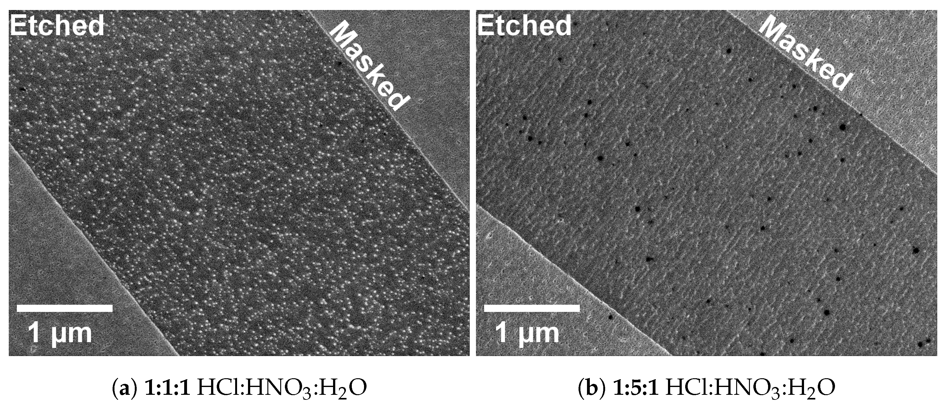
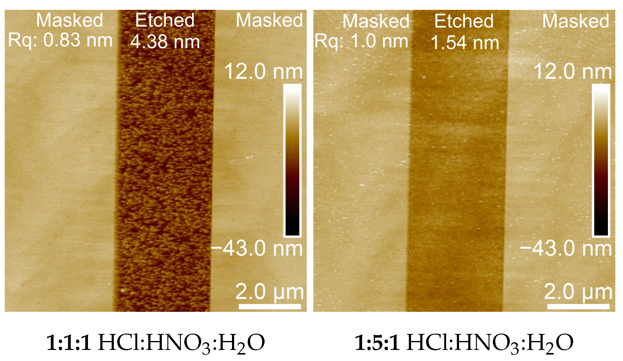
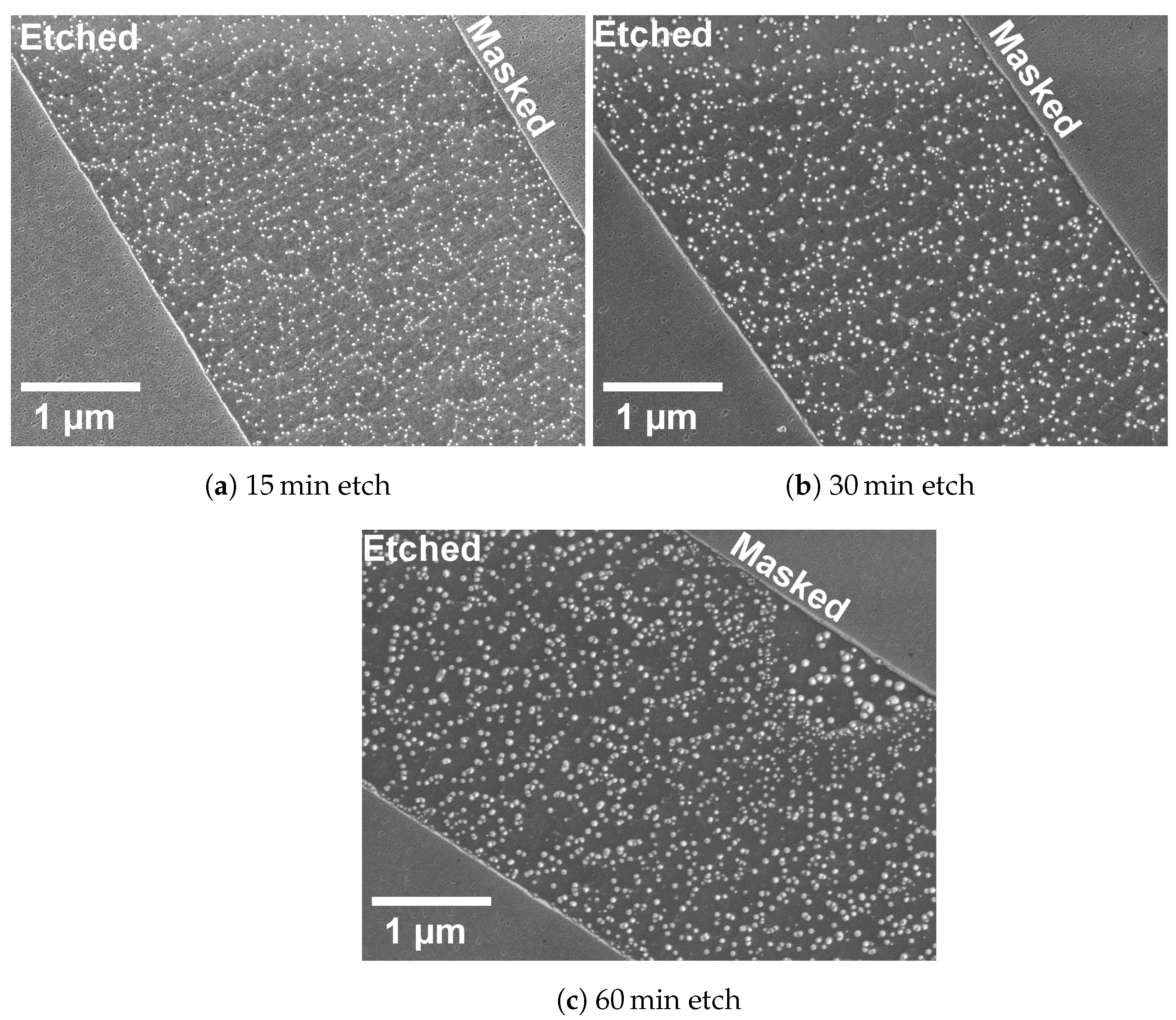
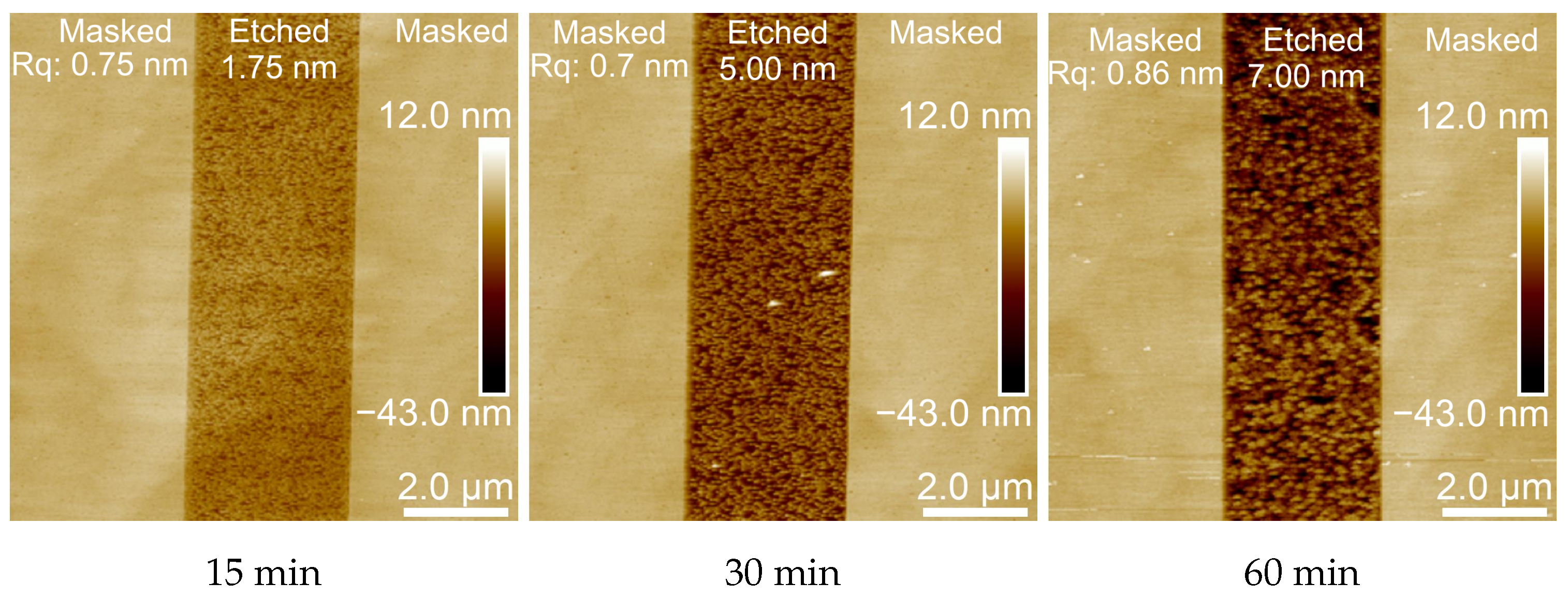
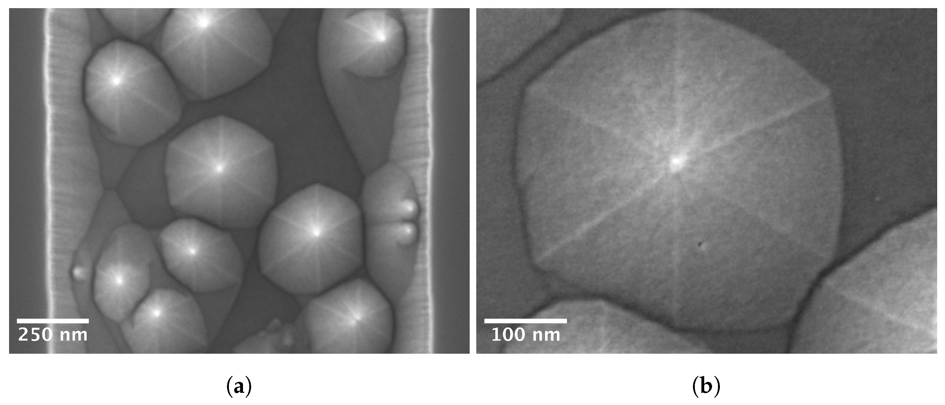
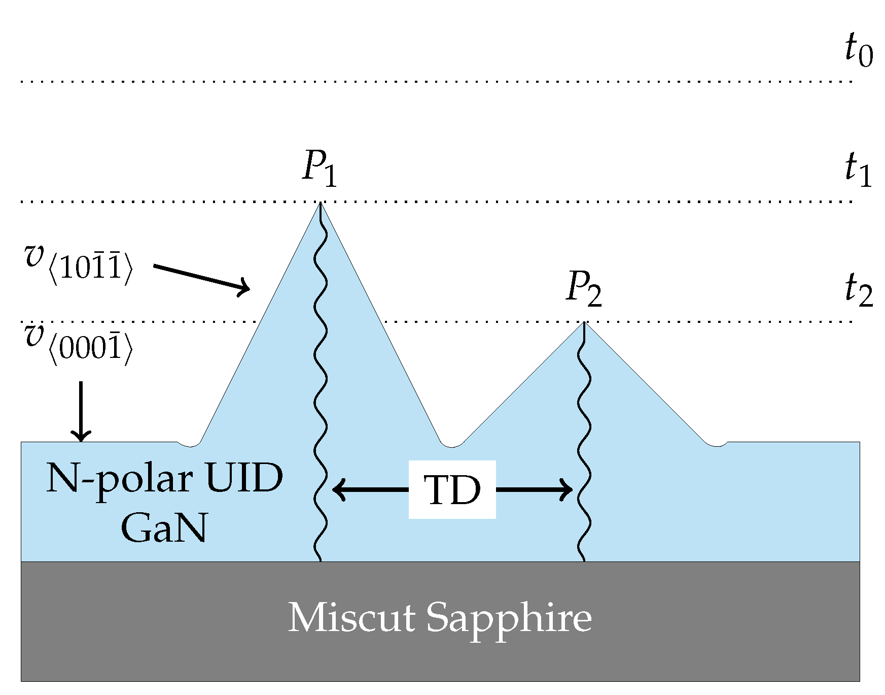
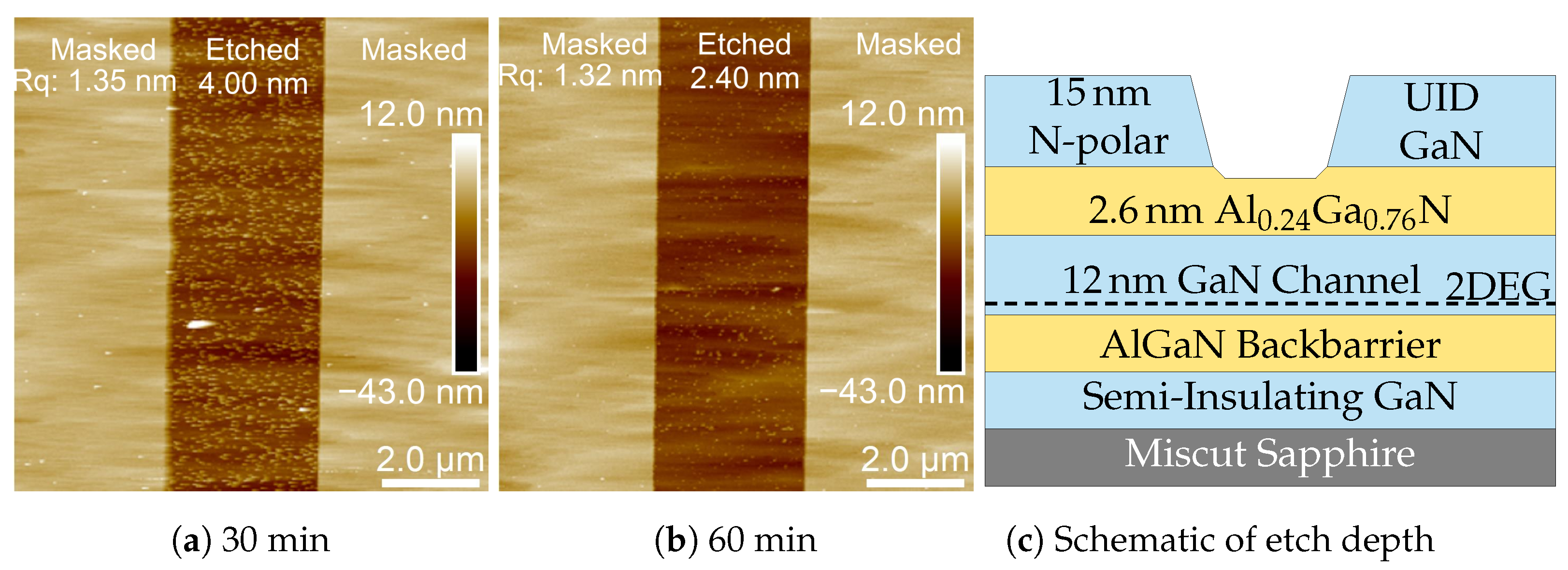
3.1. N-Polar UID GaN

The results of etching N-polar UID GaN in volume ratios of 1:1:1 and 1:5:1 of HCl:HNO3:H2O for 5 min are shown in Figure 2 and Figure 3. Figure 2a,b demonstrate that a higher nitric acid concentration results in a smoother etched surface. The black dots observed in Figure 2b are also present in the masked region, indicating that they are not related to the etching process but were present on the surface prior to etching. Subsequent discussions will focus on studies conducted using a 1:5:1 volumetric ratio of HCl:HNO3:H2O.
Figure 4 and Figure 5 present the SEM and AFM images, respectively, which depict the outcomes of etching the N-polar UID GaN samples for 15, 30, and 60 min. These images illustrate the presence of cones interspersed between the smoothly etched regions. Given the irregular surface texture presented by these etched features, the etched depth was determined by averaging the depths of the smoothly etched areas of the trench relative to the masked surface. This calculation method led to a GaN etching rate of 42 nm h 1 .
The SEM analysis quantified the density of the cones to be approximately 5 × 109 cm 2 . A key observation from the AFM data is the incremental increase in the depth of the cone tips relative to the masked surface, which increased from 1 nm after 15 min of etching to 4 nm after 60 min. This pattern indicates that the cones were etched at a rate of 4 nm h 1 .
After a thorough examination of the N-polar UID GaN sample that underwent extended etching for 12 h , as depicted in Figure 6, it was discovered that the previously identified structures were actually hexagonal pyramids. The measurements of the pyramid sidewalls revealed a 60° angle, corresponding to the { 10 1 ¯ 1 ¯ } crystal facets. We attribute the formation of the hexagonal pyramids, rather than the dodecagonal ones observed by Qi et al. [19], to differences in the surface energy, variations in the etching rates of the GaN crystal planes, the presence of defects and dislocations, and differences in the etchant concentration.
Typically, etching slows down more on the { 10 1 ¯ 1 ¯ } planes with KOH, NaOH, or HCl, resulting in the formation of hexagonal pyramids on N-polar GaN [18,21,23,24,25]. Furthermore, for Ga-polar and N-polar surfaces, heated H3PO4 and KOH produce hexagonal etch pits with { 10 1 ¯ 1 ¯ } facets that are associated with crystal defects and dislocations [15,21,25,26]. Additionally, by varying the acid concentration with H3PO4, both hexagonal and dodecagonal facets can be formed [24]. This further emphasizes the impact of the surface chemistry on the wet etching of N-polar GaN [27].
The relationship between the density of the hexagonal pyramids and the dislocation density in the N-polar UID GaN epitaxial layer lends credence to the hypothesis that these pyramids typically form at the termination sites of threading dislocations. This conclusion aligns with previous studies [15,17,18,21,22,26,28], which also observed similar phenomena in wet-etched GaN. Figure 7 graphically illustrates the pyramid evolution theory, which is further explained in [29], providing a detailed account of the etching process from its onset.
The etching process began at t 0 , targeting the N-polar GaN surface with a vertical etch in the 000 1 ¯ direction. By t 1 , a threading dislocation (TD) previously terminated within the GaN epitaxial layer at site P 1 becomes visible. This TD introduces a bifurcation in the etch rate: (1) a rate in the 000 1 ¯ direction, denoted by v 000 1 ¯ , and (2) an etch rate in the immediate vicinity of the TD, represented by v 10 1 ¯ 1 ¯ . The difference in the etch rates suggests that the 10 1 ¯ 1 ¯ plane has lower surface energy compared to the N-polar c-plane, significantly influencing the distinctive emergence of the hexagonal pyramids on the etched surface [23]. By t 2 , the etching progressed further, revealing another TD, which was etched according to the previously described etch dynamics. During this phase, the edges of pyramids P 1 and P 2 face each other and maintain their distinct profiles without intersection, as shown in Figure 6a.

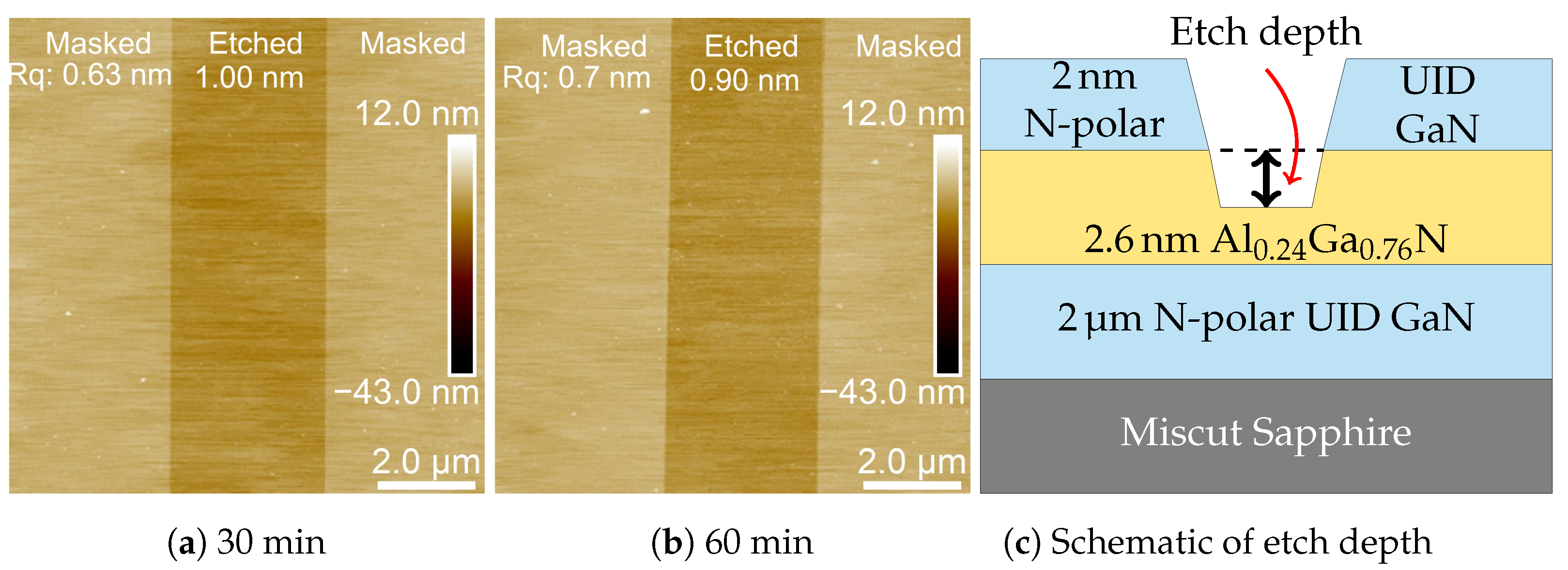
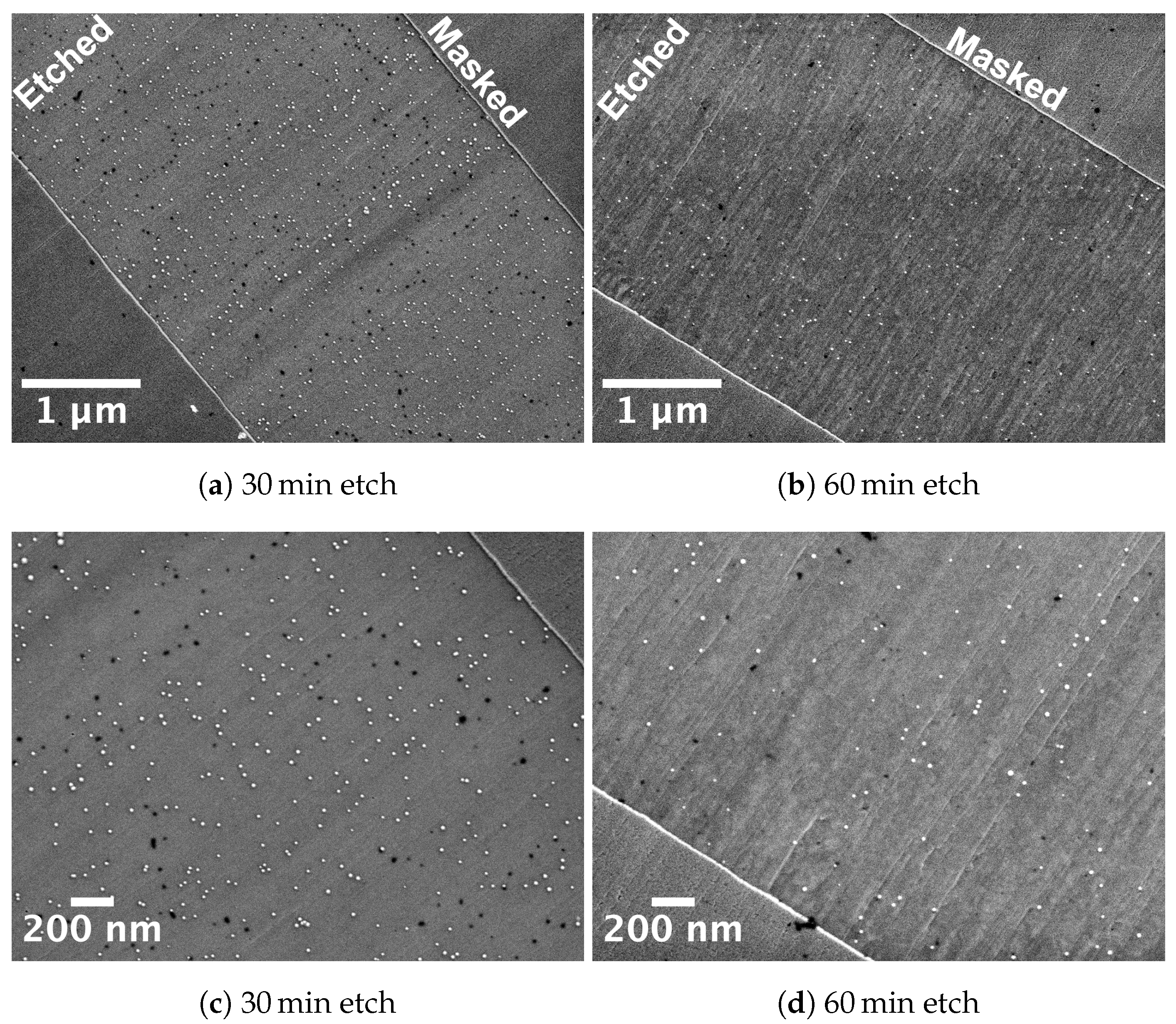
3.2. N-Polar Al0.24Ga0.76N

Figure 8 depicts the N-polar Al0.24Ga0.76N samples that were etched for 30 and 60 min. The AFM measurements depicted in Figure 9 reveal that the 2 nm GaN cap was completely removed, indicating that the SEM images captured an intact and smooth AlGaN surface. Additionally, the AlGaN surface in the images showed no signs of degradation and did not have the hexagonal pyramids that were observed in the etched N-polar GaN samples.
The AlGaN etch rate was measured to be 1 nm h 1 , which is substantially less than that of GaN. This reduction in the etch rate is primarily due to the decreased efficacy of HCl in eliminating oxidation byproducts, such as aluminum oxide. This observation aligns with the prior research on the digital etching of AlGaN that used O2 plasma and a 1:1 mixture of HCl and H2O [8]. Additionally, the significant selectivity ratio of the etchant (42:1) for GaN over AlGaN emphasizes the notably higher chemical reactivity of the N-polar GaN surface. This characteristic was also demonstrated in an ICP-RIE system using BCl3/SF6 gas chemistry, which showed a selectivity ratio of 17:1 between GaN and Al0.27Ga0.73N [30].

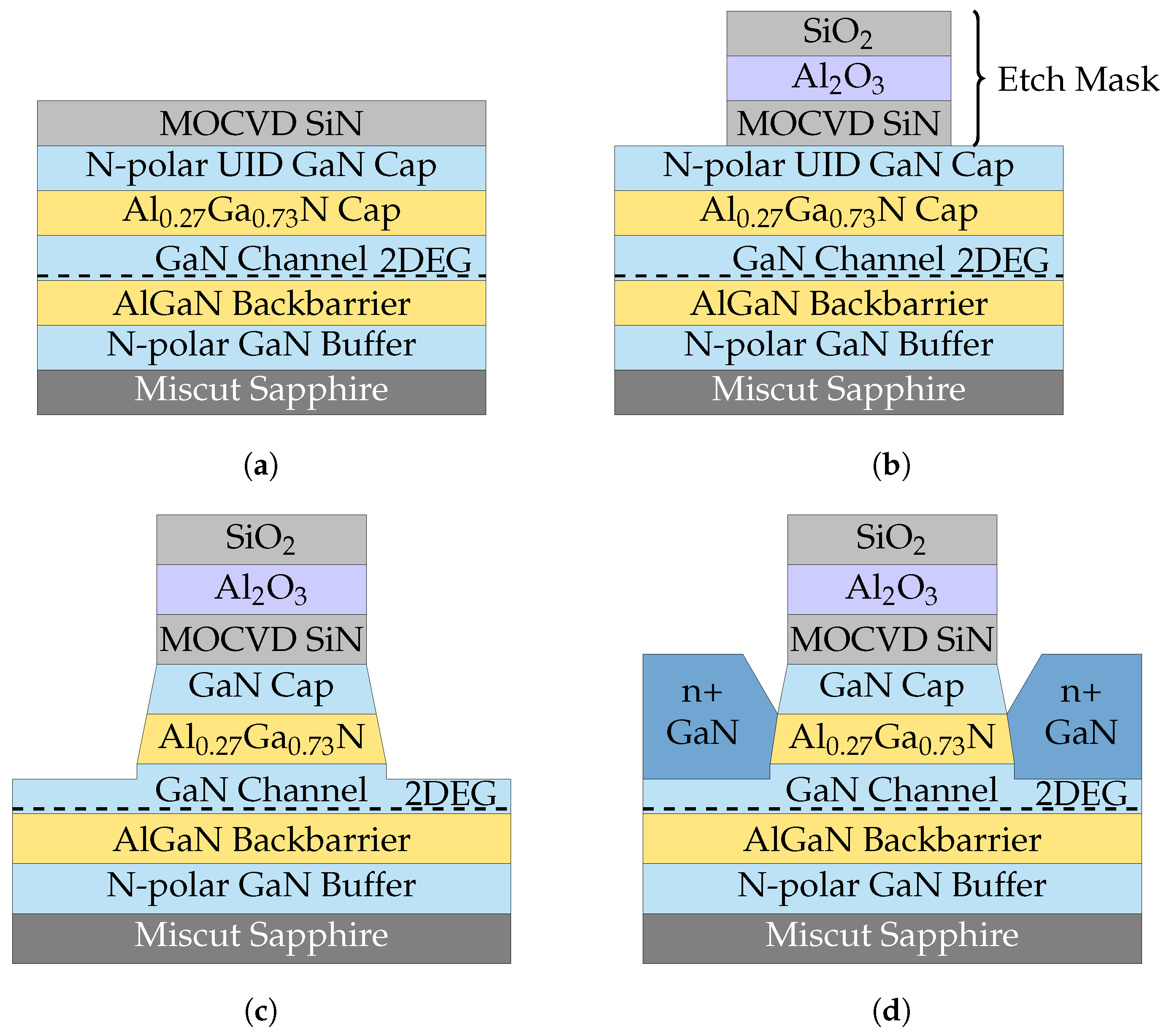
3.3. N-Polar Deep-Recess HEMT

The SEM and AFM images referenced in Figure 10 and Figure 11 show the surface of the wet-etched N-polar deep-recess HEMT. These images reveal a grainy texture on the surface, predominantly characterized by the presence of hexagonal pyramids. As shown in Figure 11c, the central objective of this etching process was to selectively remove the 15 nm N-polar UID GaN cap in the gate recess area and to halt the etching precisely at the 2.6 nm AlGaN layer. Given that the N-polar UID GaN has an etch rate of 42 nm h 1 , a calculated etching duration of 21 min was deemed sufficient for removing the GaN cap, with an additional 9 min allowed for over-etching to ensure thorough removal. This methodological approach was confirmed to be effective at the 30 min etching checkpoint, as evidenced by the complete removal of the GaN cap in Figure 10a.
Further examination of Figure 10d reveals that, after an additional over-etching period of 39 min (228% over-etch), there was a significant reduction in both the size and density of the hexagonal pyramids. This observation contrasts with the smooth etched AlGaN structure, suggesting that the presence of the residual pyramids on the HEMT surface is largely due to the 15 nm thick GaN cap. The formation of these pyramids appeared to be a gradual process throughout the etching duration, which was influenced by the thickness of the GaN cap. However, the high selectivity of the etchant allows for extensive over-etching, which effectively reduces the pyramid size without adversely impacting the AlGaN layer, showcasing the precision and control achievable using this wet etchant. Given this distinctiveness, the etchant holds promise for aiding the fabrication of N-polar deep-recess HEMTs. Specifically, it could be beneficial for HEMT structures, such as the one referenced in [4], which features a 20 nm GaN cap.

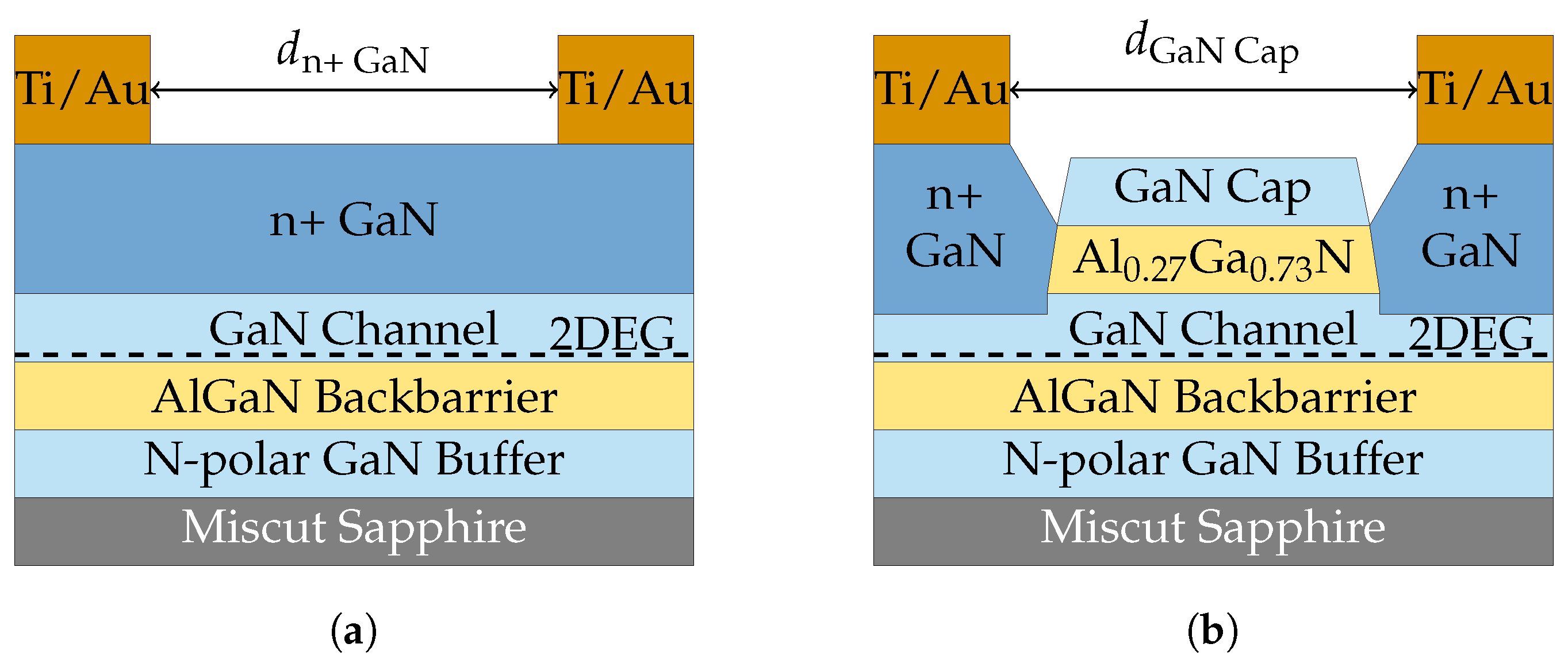
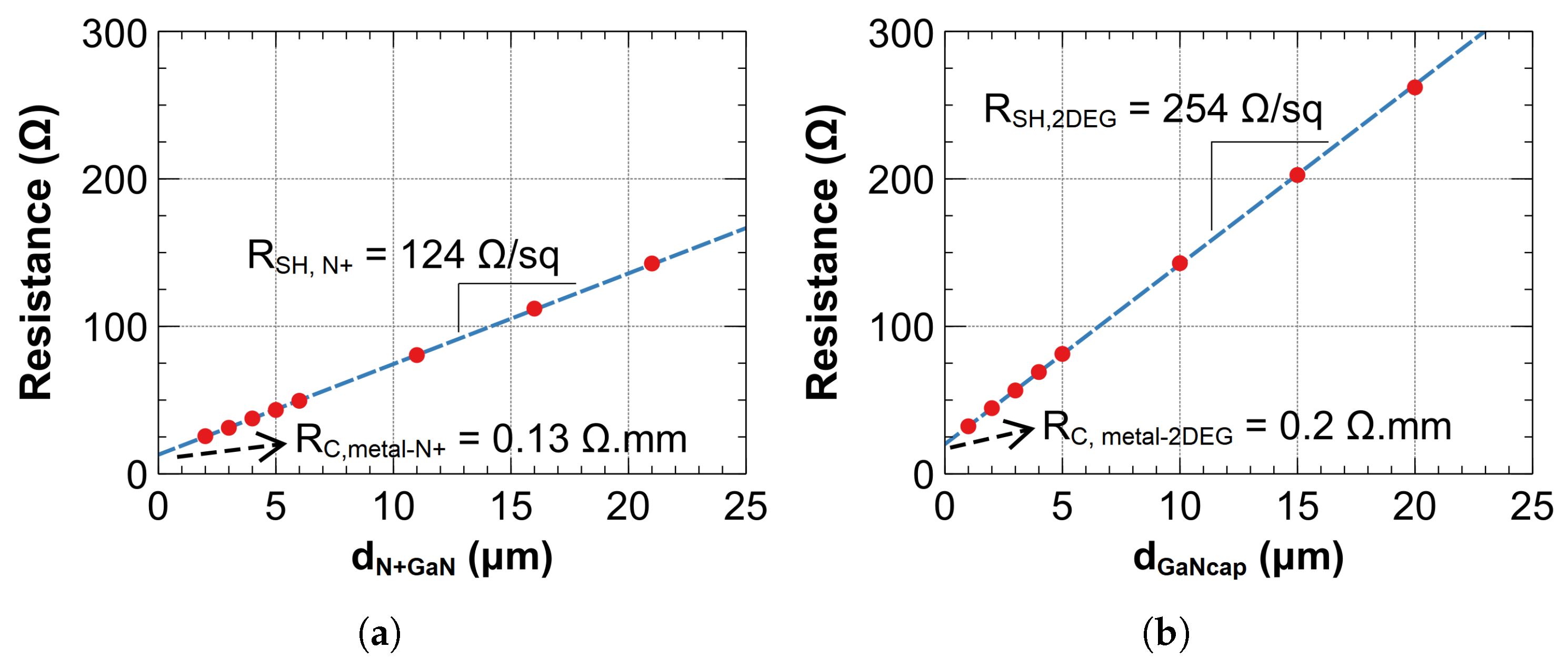
3.4. NPDR HEMT Transmission Line Measurement Structures

The selective wet etching of the GaN cap in the HEMT fabrication process offers significant advantages, particularly in the n+ GaN regrowth process, for optimizing the source and drain contacts. To explore this application, an experiment was conducted using a deep-recess HEMT wafer with a 20 nm GaN cap, as detailed in the process flow illustrated in Figure 12. The procedure began by depositing an etch hard mask stack composed of 11 nm of ALD Al2O3 and 225 nm of PECVD SiO2. This was followed by the optical patterning of the hard mask over the designated regions for n+ regrowth. The subsequent etching steps involved the use of ICP CHF3/CF4/O2 for the SiO2 layer, which was stopped on the Al2O3 etch stop layer. This etch stop layer was then removed with dilute TMAH, and SiN was removed using ICP CF4/O2.
After the completion of the hard-mask etching, an aqueous mixture of HCl (1 HCl:5 HNO3:1 H2O) was utilized to selectively etch away the GaN cap, leaving the Al0.27Ga0.73N layer intact. A BCl3/Cl2-based RIE process was used to etch the Al0.27Ga0.73N cap. This process culminated in the regrowth of 10 nm of UID GaN and 40 nm of n+ GaN using Molecular Beam Epitaxy. The etch hard mask was subsequently removed using HF, followed by the deposition of Ti/Au metal contacts for the n+ GaN and GaN cap transmission line measurement (TLM) structures, as shown in Figure 13.
Figure 14 shows the results of the TLM tests, which revealed the key electrical properties of the fabricated structures. Specifically, the metal to n+ contact resistance ( R C , metal-n+) and the metal to two-dimensional electron gas (2DEG) contact resistance ( R C , metal-2DEG) were measured to be 0.13 Ω mm and 0.20 Ω mm, respectively. This is noteworthy when compared to the 0.18 Ω mm metal to 2DEG contact resistance observed in the n+ GaN ohmic regrowth of a 20 nm GaN-capped NPDR HEMT fabricated via ICP, as reported in previous studies [4]. Thus, with this wet-etching technique, high-throughput device fabrication can be achieved without sacrificing the device performance.
Further analysis focused on the resistance of the n+ GaN region situated between the metal contacts and the onset region of the GaN cap. The contact resistance from the 2DEG to n+ ( R C , 2DEG-n+) was derived to be low 0.02 Ω mm. This result demonstrates the suitability of the selective wet GaN etch process for the n+ GaN regrowth step, confirming its utility as a fabrication technique for state-of-the-art HEMTs.

4. Conclusions

In this study, we investigated the effects of etching N-polar UID GaN, GaN/AlGaN heterostructures, and deep-recess high-electron-mobility transistor (HEMT) structures using an aqueous etchant composed of HCl, HNO3, and H2O in a volume ratio of 1:5:1 for various durations. Our findings revealed that etching N-polar GaN led to the formation of distinctive hexagonal pyramids characterized by { 10 1 ¯ 1 ¯ } facets. The wet etch showed a high selectivity ratio of 42:1 for N-polar GaN relative to AlGaN during the etching process. This selectivity was further demonstrated through the successful etching of an N-polar deep-recess HEMT structure, precisely stopping at the 2.6 nm AlGaN layer, which highlights the precision of the technique. Moreover, we utilized this selective wet-etching approach in the n+ GaN regrowth process to develop contacts, achieving contact resistances on par with those observed in the dry-etched samples. This outcome validates that the GaN cap was effectively etched without detrimentally affecting the contact quality. Therefore, it is anticipated that the integration of this etching approach into future research on GaN HEMT fabrication will significantly broaden the array of available processing capabilities and options.

Author Contributions

Conceptualization, E.K., E.A., and B.R.; Methodology, E.K. and E.A.; Formal Analysis, E.K. and E.A.; Investigation, E.K. and E.A.; Resources, I.S., N.H., and S.K.; Writing—Original Draft Preparation, E.K. and E.A.; Data Curation, E.K. and E.A.; Writing—Review and Editing, K.K., H.C., B.R., and U.K.M.; Visualization, E.K. and E.A.; Supervision, B.R.; Project Administration, B.R.; Funding Acquisition, U.K.M. All authors have read and agreed to the published version of the manuscript.

Funding

This research was funded by Office of Naval Research under grant number N00014-20-1-2166 and National Science Foundation California LSAMP Bridge to the Doctorate Fellowship under Grant No. HRD-1701365.

Data Availability Statement

The data that support the findings of this study are available within the article. More detailed findings of this study are available from the corresponding author upon reasonable request.

Acknowledgments

A portion of this work was conducted in the UCSB Nanofabrication Facility, an open-access laboratory.

Conflicts of Interest

The authors declare no conflicts of interest.

References

  1. Wong, M.H.; Keller, S.; Nidhi; Dasgupta, S.; Denninghoff, D.J.; Kolluri, S.; Brown, D.F.; Lu, J.; Fichtenbaum, N.A.; Ahmadi, E.; et al. N-polar GaN epitaxy and high electron mobility transistors. Semicond. Sci. Technol. 2013, 28, 074009. [Google Scholar] [CrossRef]
  2. Romanczyk, B.; Wienecke, S.; Guidry, M.; Li, H.; Ahmadi, E.; Zheng, X.; Keller, S.; Mishra, U.K. Demonstration of Constant 8 W/mm Power Density at 10, 30, and 94 GHz in State-of-the-Art Millimeter-Wave N-Polar GaN MISHEMTs. IEEE Trans. Electron Devices 2018, 65, 45–50. [Google Scholar] [CrossRef]
  3. Akso, E.; Collins, H.; Clymore, C.; Li, W.; Guidry, M.; Romanczyk, B.; Wurm, C.; Liu, W.; Hatui, N.; Hamwey, R.; et al. First Demonstration of Four-Finger N-polar GaN HEMT Exhibiting Record 712-mW Output Power With 31.7% PAE at 94 GHz. IEEE Microw. Wirel. Technol. Lett. 2023, 33, 683–686. [Google Scholar] [CrossRef]
  4. Li, W.; Romanczyk, B.; Guidry, M.; Akso, E.; Hatui, N.; Wurm, C.; Liu, W.; Shrestha, P.; Collins, H.; Clymore, C.; et al. Record RF Power Performance at 94 GHz From Millimeter-Wave N-Polar GaN-on-Sapphire Deep-Recess HEMTs. IEEE Trans. Electron Devices 2023, 70, 2075–2080. [Google Scholar] [CrossRef]
  5. Buttari, D.; Chini, A.; Chakraborty, A.; Mccarthy, L.; Xing, H.; Palacios, T.; Shen, L.; Keller, S.; Mishra, U.K. Selective dry etching of Gan over Algan in Bcl3/SF6 mixtures. Int. J. High Speed Electron. Syst. 2004, 14, 756–761. [Google Scholar] [CrossRef]
  6. Pearton, S.J.; Shul, R.J.; Ren, F. A Review of Dry Etching of GaN and Related Materials. Mrs Internet J. Nitride Semicond. Res. 2000, 5, e11. [Google Scholar] [CrossRef]
  7. Cuerdo, R.; Pei, Y.; Chen, Z.; Keller, S.; DenBaars, S.P.; Calle, F.; Mishra, U.K. The Kink Effect at Cryogenic Temperatures in Deep Submicron AlGaN/GaN HEMTs. IEEE Electron Device Lett. 2009, 30, 209–212. [Google Scholar] [CrossRef]
  8. Buttari, D.; Heikman, S.; Keller, S.; Mishra, U.K. Digital Etching for Highly Reproducible Low Damage Gate Recessing on AlGaN/GaN HEMTs. In Proceedings of the IEEE Lester Eastman Conference on High Performance Devices, Newark, DE, USA, 8 August 2002; pp. 461–469. [Google Scholar] [CrossRef]
  9. Burnham, S.D.; Boutros, K.; Hashimoto, P.; Butler, C.; Wong, D.W.; Hu, M.; Micovic, M. Gate-recessed normally-off GaN-on- Si HEMT using a new O2-BCl3 digital etching technique. Phys. Status Solidi 2010, 7, 2010–2012. [Google Scholar] [CrossRef]
  10. Wu, J.; Lei, S.; Cheng, W.C.; Sokolovskij, R.; Wang, Q.; Xia, G.M.; Yu, H. Oxygen-based digital etching of AlGaN/GaN structures with AlN as etch-stop layers. J. Vac. Sci. Technol. Vacuum. Surfaces Film. 2019, 37, 060401. [Google Scholar] [CrossRef]
  11. Ruel, S.; Pimenta-Barros, P.; Roux, F.L.; Chauvet, N.; Massardier, M.; Thoueille, P.; Tan, S.; Shin, D.; Gaucher, F.; Posseme, N. Atomic layer etching of GaN using Cl2 and He or Ar plasma. J. Vac. Sci. Technol. Vacuum. Surfaces Film. 2021, 39, 022601. [Google Scholar] [CrossRef]
  12. Shih, P.C.; Engel, Z.; Ahmad, H.; Doolittle, W.A.; Palacios, T. Wet-based digital etching on GaN and AlGaN. Appl. Phys. Lett. 2022, 120, 022101. [Google Scholar] [CrossRef]
  13. Ho, W.Y.; Chow, Y.C.; Biegler, Z.; Qwah, K.S.; Tak, T.; Wissel-Garcia, A.; Liu, I.; Wu, F.; Nakamura, S.; Speck, J.S. Atomic layer etching (ALE) of III-nitrides. Appl. Phys. Lett. 2023, 123, 062102. [Google Scholar] [CrossRef]
  14. Zhuang, D.; Edgar, J. Wet etching of GaN, AlN, and SiC: A review. Mater. Sci. Eng. Rep. 2005, 48, 1–46. [Google Scholar] [CrossRef]
  15. Visconti, P.; Huang, D.; Reshchikov, M.; Yun, F.; Cingolani, R.; Smith, D.; Jasinski, J.; Swider, W.; Liliental-Weber, Z.; Morkoç, H. Investigation of defects and surface polarity in GaN using hot wet etching together with microscopy and diffraction techniques. Mater. Sci. Eng. 2002, 93, 229–233. [Google Scholar] [CrossRef]
  16. Fujii, T.; Gao, Y.; Sharma, R.; Hu, E.L.; DenBaars, S.P.; Nakamura, S. Increase in the extraction efficiency of GaN-based light-emitting diodes via surface roughening. Appl. Phys. Lett. 2004, 84, 855–857. [Google Scholar] [CrossRef]
  17. Gao, Y.; Fujii, T.; Sharma, R.; Fujito, K.; Denbaars, S.P.; Nakamura, S.; Hu, E.L. Roughening Hexagonal Surface Morphology on Laser Lift-Off (LLO) N-Face GaN with Simple Photo-Enhanced Chemical Wet Etching. Jpn. J. Appl. Phys. 2004, 43, L637. [Google Scholar] [CrossRef]
  18. Gao, Y.; Craven, M.D.; Speck, J.S.; Baars, S.P.D.; Hu, E.L. Dislocation- and crystallographic-dependent photoelectrochemical wet etching of gallium nitride. Appl. Phys. Lett. 2004, 84, 3322–3324. [Google Scholar] [CrossRef]
  19. Qi, S.L.; Chen, Z.Z.; Fang, H.; Sun, Y.J.; Sang, L.W.; Yang, X.L.; Zhao, L.B.; Tian, P.F.; Deng, J.J.; Tao, Y.B.; et al. Study on the formation of dodecagonal pyramid on nitrogen polar GaN surface etched by hot H3PO4. Appl. Phys. Lett. 2009, 95, 071114. [Google Scholar] [CrossRef]
  20. Keller, S.; DenBaars, S.P. Metalorganic chemical vapor deposition of group III nitrides—A discussion of critical issues. J. Cryst. Growth 2003, 248, 479–486. [Google Scholar] [CrossRef]
  21. Han, S.C.; Kim, J.K.; Kim, J.Y.; Kim, K.K.; Tampo, H.; Niki, S.; Lee, J.M. Formation of Hexagonal Pyramids and Pits on V-/VI-Polar and III-/II-Polar GaN/ZnO Surfaces by Wet Etching. J. Electrochem. Soc. 2010, 157, D60. [Google Scholar] [CrossRef]
  22. Keller, S.; Fichtenbaum, N.A.; Wu, F.; Brown, D.; Rosales, A.; DenBaars, S.P.; Speck, J.S.; Mishra, U.K. Influence of the substrate misorientation on the properties of N-polar GaN films grown by metal organic chemical vapor deposition. J. Appl. Phys. 2007, 102, 083546. [Google Scholar] [CrossRef]
  23. Ng, H.M.; Weimann, N.G.; Chowdhury, A. GaN nanotip pyramids formed by anisotropic etching. J. Appl. Phys. 2003, 94, 650–653. [Google Scholar] [CrossRef]
  24. Jung, Y.; Ahn, J.; Baik, K.H.; Kim, D.; Pearton, S.J.; Ren, F.; Kim, J. Chemical Etch Characteristics of N-Face and Ga-Face GaN by Phosphoric Acid and Potassium Hydroxide Solutions. J. Electrochem. Soc. 2011, 159, H117–H120. [Google Scholar] [CrossRef]
  25. Wang, L.; Ma, J.; Liu, Z.; Yi, X.; Yuan, G.; Wang, G. N-polar GaN etching and approaches to quasi-perfect micro-scale pyramid vertical light-emitting diodes array. J. Appl. Phys. 2013, 114, 133101. [Google Scholar] [CrossRef]
  26. Stocker, D.A.; Schubert, E.F.; Redwing, J.M. Crystallographic wet chemical etching of GaN. Appl. Phys. Lett. 1998, 73, 2654–2656. [Google Scholar] [CrossRef]
  27. Li, D.; Sumiya, M.; Fuke, S.; Yang, D.; Que, D.; Suzuki, Y.; Fukuda, Y. Selective etching of GaN polar surface in potassium hydroxide solution studied by x-ray photoelectron spectroscopy. J. Appl. Phys. 2001, 90, 4219–4223. [Google Scholar] [CrossRef]
  28. Weyher, J.; Brown, P.; Rouvière, J.; Wosinski, T.; Zauner, A.; Grzegory, I. Recent advances in defect-selective etching of GaN. J. Cryst. Growth 2000, 210, 151–156. [Google Scholar] [CrossRef]
  29. Sangwal, K. Etching of crystals: Theory, experiment, and application. In Defects in Solids; v. 15; North-Holland: Amsterdam, The Netherlands, 1987; Volume 15. [Google Scholar]
  30. Wienecke, S.; Romanczyk, B.; Guidry, M.; Li, H.; Zheng, X.; Ahmadi, E.; Hestroffer, K.; Megalini, L.; Keller, S.; Mishra, U.K. N-Polar Deep Recess MISHEMTs With Record 2.9 W/mm at 94 GHz. IEEE Electron Device Lett. 2016, 37, 713–716. [Google Scholar] [CrossRef]
Figure 1. Layer structure of investigated N-polar GaN samples: (a) N-polar UID GaN, (b) 20 nm N-polar Al 0.24 Ga 0.76 N with a 2 nm N-polar UID GaN top layer, and (c) N-polar deep-recess HEMT.
Crystals 14 00485 g001
Figure 2. SEM images of volumetric study of N-polar UID GaN after wet etching: (a) higher concentration of HNO3 in etch mixture (b) results in a smoother etched surface for N-polar GaN.
Crystals 14 00485 g002
Figure 3. AFM images of volumetric study of N-polar UID GaN.
Crystals 14 00485 g003
Figure 4. SEM images of N-polar UID GaN after wet etching: displaying surface morphologies at 15, 30, and 60 min etching intervals (ac).
Crystals 14 00485 g004
Figure 5. AFM images of etched N-polar UID GaN samples: 15, 30, and 60 min etch times.
Crystals 14 00485 g005
Figure 6. SEM images of 12 h etched N-polar UID GaN: (a) low-resolution scan showing hexagonal pyramids formed by wet etch. (b) High-resolution scan revealing six-sided { 10 1 ¯ 1 ¯ } crystal facets.
Crystals 14 00485 g006
Figure 7. Schematic diagram showing the formation of the hexagonal pyramids’ over-etch times.
Crystals 14 00485 g007
Figure 8. SEM images of N-polar AlGaN after wet etching, showing surface morphologies at 30 and 60 min (a,b) and high-resolution examinations (c,d), revealing post-removal smoothness of 2 nm N-polar UID GaN cap.
Crystals 14 00485 g008
Figure 9. AFM images of the wet-etched AlGaN samples at 30 and 60 min: (a,b) illustrate the initial targeting of the 2 nm thick N-polar UID GaN layer, followed by slower etching through the AlGaN layer (c).
Crystals 14 00485 g009
Figure 10. SEM images of N-polar deep-recess HEMT after wet etching: displaying surface morphologies at 30 and 60 min (a,b), with detailed high-resolution views (c,d), illustrating the diminishing surface roughness as the 15 nm N-polar UID GaN layer is etched away, revealing the undisturbed AlGaN surface beneath.
Crystals 14 00485 g010
Figure 11. (a,b) AFM images of wet-etched AlGaN samples etched for 30 and 60 min, respectively. (c) Illustrates that the 15 nm N-polar UID GaN is etched through and stops short on the AlGaN surface.
Crystals 14 00485 g011
Figure 12. (a) Deep-recess HEMT epitaxial layer formation. (b) GaN etch mask application and patterning. (c) Selective wet etching of GaN cap and RIE of AlGaN cap. (d) MBE regrowth of layered GaN: 10 nm UID GaN layer topped with 40 nm n+ GaN.
Crystals 14 00485 g012
Figure 13. TLM structures for the evaluation of (a) metal to n+ GaN contact resistance ( R C , metal-n+). (b) Metal to 2DEG ( R C , metal-2DEG) and 2DEG to n+ ( R C , 2DEG-n+) contact resistances.
Crystals 14 00485 g013
Figure 14. Resistance vs. spacing for (a) n+ TLM structure to evaluate metal to n+ GaN contact resistance ( R C , metal-n+) and (b) access region TLM structure to evaluate metal to 2DEG ( R C , metal-2DEG) and 2DEG to n+ ( R C , 2DEG-n+) contact resistances.
Crystals 14 00485 g014
Disclaimer/Publisher’s Note: The statements, opinions and data contained in all publications are solely those of the individual author(s) and contributor(s) and not of MDPI and/or the editor(s). MDPI and/or the editor(s) disclaim responsibility for any injury to people or property resulting from any ideas, methods, instructions or products referred to in the content.

