

MOCVD-grown β-Ga2O3 as a Gate Dielectric on AlGaN/GaN-Based Heterojunction Field Effect Transistor

 ,
,  ,
, 
Abstract
1. Introduction
2. Experimental Methods
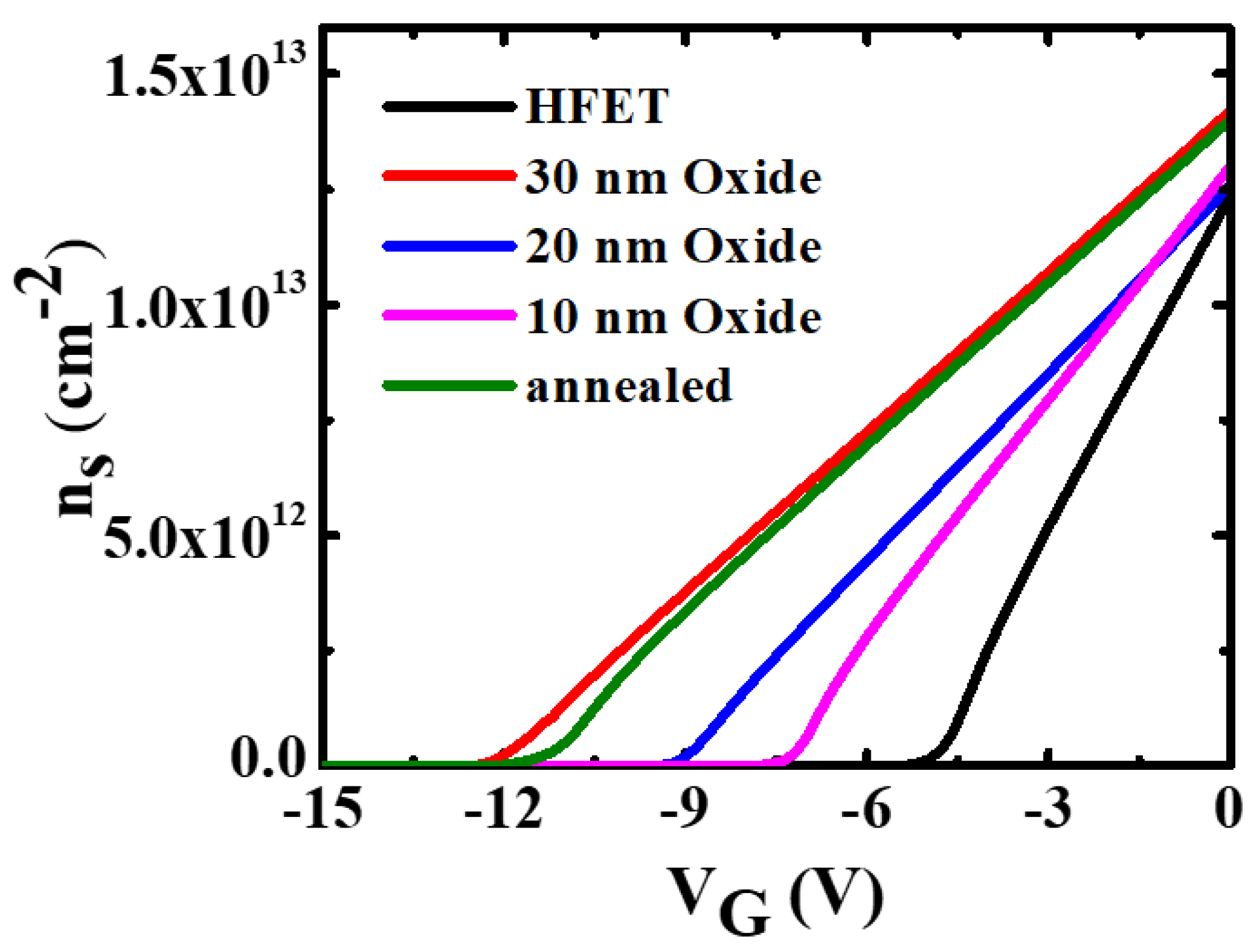
3. Results and Discussions
4. Conclusions
Supplementary Materials
Author Contributions
Funding
Data Availability Statement
Acknowledgments
Conflicts of Interest
References
- Morkoç, H. Handbook of Nitride Semiconductors and Devices, Materials Properties, Physics and Growth; Wiley-VCH: Weinhem, Germany, 2009; ISBN 9783527408375. [Google Scholar]
- Mohammad, S.N.; Salvador, A.A.; Morkoc, H. Emerging gallium nitride-based devices. Proc. IEEE. 1995, 83, 1306–1355. [Google Scholar] [CrossRef]
- Morkoç, H. Nitride Semiconductors and Devices; Springer: Berlin/Heidelberg, Germany; New York, NY, USA, 1999; ISBN 3-540-64038. [Google Scholar]
- Zeng, F.; An, J.X.; Zhou, G.; Li, W.; Wang, H.; Duan, T.; Jiang, L.; Yu, H. A Comprehensive Review of Recent Progress on GaN High Electron Mobility Transistors: Devices, Fabrication and Reliability. Electronics 2018, 7, 377. [Google Scholar] [CrossRef]
- Islam, N.; Mohamed, M.F.P.; Khan, M.F.A.J.; Falina, S.; Kawarada, H.; Syamsul, M. Reliability, Applications and Challenges of GaN HEMT Technology for Modern Power Devices: A Review. Crystals 2022, 12, 1581. [Google Scholar] [CrossRef]
- Kim, H.; Lee, J.; Liu, D.; Lu, W. Gate Current Leakage and Breakdown Mechanism in Unpassivated AlGaNGaN High Electron Mobility Transistors by Post-Gate Annealing. Appl. Phys. Lett. 2005, 86, 143505. [Google Scholar] [CrossRef]
- Leach, J.H.; Morkoç, H. Status of Reliability of GaN-Based Heterojunction Field Effect Transistors. Proc. IEEE 2010, 98, 1127–1139. [Google Scholar] [CrossRef]
- Rao, G.P.; Singh, R.; Lenka, T.R. Performance Analysis of AlGaN/GaN HEMT for RF and Microwave Nanoelectronics Applications. In HEMT Technology and Applications; Springer Nature: Singapore, 2023; pp. 139–153. [Google Scholar] [CrossRef]
- Trew, R.J. Wide bandgap semiconductor transistors for microwave power amplifiers. IEEE Microw. Mag. 2000, 1, 46–54. [Google Scholar] [CrossRef]
- Brar, B.; Boutros, K.; DeWarnes, R.E.; Tilak, V.; Shealy, R.; Eastman, L. Impact ionization in high performance AlGaN/GaN HEMTs. In Proceedings of the IEEE Lester Eastman Conference on High Performance Devices, Newark, DE, USA, 8 August 2002; pp. 487–491. [Google Scholar]
- Trew, R.J.; Green, D.S.; Shealy, J.B. AlGaN/GaN HFET reliability. IEEE Microw. Mag. 2009, 10, 116–127. [Google Scholar] [CrossRef]
- Zhou, H.; Lou, X.; Sutherlin, K.; Summers, J.; Kim, S.B.; Chabak, K.D.; Gordon, R.G.; Ye, P.D. DC and RF Performance of AlGaN/GaN/SiC MOSHEMTs with Deep Sub-Micron T-Gates and Atomic Layer Epitaxy MgCaO as Gate Dielectric. IEEE Electron Device Lett. 2017, 38, 1409–1412. [Google Scholar] [CrossRef]
- Liu, C.; Chor, E.F.; Tan, L.S. Investigations of HfO2∕AlGaN∕GaN metal-oxide-semiconductor high electron mobility transistors. Appl. Phys. Lett. 2006, 88, 173504. [Google Scholar] [CrossRef]
- Asubar, J.T.; Yatabe, Z.; Gregusova, D.; Hashizume, T. Controlling surface/interface states in GaN-based transistors: Surface model, insulated gate, and surface passivation. J. Appl. Physics. 2021, 129, 121102. [Google Scholar] [CrossRef]
- Ramanan, N.; Lee, B.; Misra, V. Accurate characterization and understanding of interface trap density trends between atomic layer deposited dielectrics and AlGaN/GaN with bonding constraint theory. Appl. Phys. Lett. 2015, 106, 243503. [Google Scholar] [CrossRef]
- Gusev, E.P.; Copel, M.; Cartier, E.; Baumvol, I.J.; Krug, C.; Gribelyuk, M.A. High-resolution depth profiling in ultrathin Al2O3 films on Si. Appl. Phys. Letters. 2000, 76, 176–178. [Google Scholar] [CrossRef]
- Lee, B.H.; Kang, L.; Nieh, R.; Qi, W.J.; Lee, J.C. Thermal stability and electrical characteristics of ultrathin hafnium oxide gate dielectric reoxidized with rapid thermal annealing. Appl. Phys. Letters. 2000, 76, 1926–1928. [Google Scholar] [CrossRef]
- Copel, M.; Gribelyuk, M.; Gusev, E. Structure and stability of ultrathin zirconium oxide layers on Si (001). Appl. Phys. Letters. 2000, 76, 436–438. [Google Scholar] [CrossRef]
- Husna, F.; Lachab, M.; Sultana, M.; Adivarahan, V.; Fareed, Q.; Khan, A. High-Temperature Performance of AlGaN/GaN MOSHEMT with SiO2 Gate Insulator Fabricated on Si (111) Substrate. IEEE Trans. Electron Devices 2012, 59, 2424–2429. [Google Scholar] [CrossRef]
- Illarionov, Y.Y.; Rzepa, G.; Waltl, M.; Knobloch, T.; Grill, A.; Marco, M.; Furchi, M.M.; Mueller, T.; Grasser, T. The role of charge trapping in MoS2/SiO2 and MoS2/hBN field-effect transistors. 2d Mater. 2016, 3, 035004. [Google Scholar] [CrossRef]
- Balakrishnan, G.; Babu, R.V.; Shin, K.S.; Song, J.I. Growth of highly oriented γ-and α-Al2O3 thin films by pulsed laser deposition. Opt. Laser Technol. 2014, 56, 317–321. [Google Scholar] [CrossRef]
- Khan, M.F.; Rehman, S.; Akhtar, I.; Aftab, S.; Ajmal, H.M.S.; Khan, W.; Kim, D.-k.; Eom, J. High mobility ReSe2 field effect transistors: Schottky-barrier-height-dependent photoresponsivity and broadband light detection with Co decoration. 2d Mater. 2019, 7, 015010. [Google Scholar] [CrossRef]
- Passlack, M.; Schubert, E.F.; Hobson, W.S.; Hong, M.; Moriya, N.; Chu, S.N.; Konstadinidis, K.; Mannaerts, J.P.; Schnoes, M.L.; Zydzik, G.J. Ga2O3 films for electronic and optoelectronic applications. J. Appl. Phys. 1995, 77, 686–693. [Google Scholar] [CrossRef]
- Green, A.J.; Speck, J.; Xing, G.; Moens, P.; Allerstam, F.; Gumaelius, K.; Neyer, T.; Arias-Purdue, A.; Mehrotra, V.; Kuramata, A.; et al. β-Gallium Oxide Power Electronics. APL Mater 2022, 10, 029201. [Google Scholar] [CrossRef]
- Choi, D.W.; Chung, K.B.; Park, J.S. Low temperature Ga2O3 atomic layer deposition using gallium tri-isopropoxide and water. Thin Solid Films 2013, 546, 31–34. [Google Scholar] [CrossRef]
- Donmez, I.; Ozgit-Akgun, C.; Biyikli, N. Low temperature deposition of Ga2O3 thin films using trimethylgallium and oxygen plasma. J. Vac. Sci. Technol. A Vac. Surf. Films 2013, 31, 01A110. [Google Scholar] [CrossRef]
- Hashizume, T.; Nishiguchi, K.; Kaneki, S.; Kuzmik, J.; Yatabe, Z. State of the Art on Gate Insulation and Surface Passivation for GaN-Based Power HEMTs. Mater. Sci. Semicond. Process. 2018, 78, 85–95. [Google Scholar] [CrossRef]
- Hasan, S.; Mamun, A.; Hussain, K.; Gaevski, M.; Ahmad, I.; Khan, A. Growth Evolution of High-Quality MOCVD Aluminum Nitride Using Nitrogen as Carrier Gas on the Sapphire Substrate. J. Mater. Res. 2021, 36, 4360–4369. [Google Scholar] [CrossRef]
- Hasan, S.; Mamun, A.; Hussain, K.; Patel, D.; Gaevski, M.; Ahmad, I.; Khan, A. Investigation of MOCVD Grown Crack-Free 4 Μm Thick Aluminum Nitride Using Nitrogen as a Carrier Gas. MRS Adv. 2021, 6, 456–460. [Google Scholar] [CrossRef]
- Shrestha, N.; Shrestha, N.M.; Wang, Y.Y.; Li, Y.; Chang, E.Y. Effect of AlN Spacer Layer on AlGaN/GaN HEMTs. In Proceedings of the 16th International Workshop on Computational Electronics, Nara, Japan, 4–7 June 2013; ISBN 978-3-901578-26-7. [Google Scholar]
- Hubáček, T.; Hospodková, A.; Kuldová, K.; Zíková, M.S.; Pangrác, J.; Čížek, J.; Liedke, M.O.; Butterilng, M.; Wagner, A.; Hubík, P.; et al. Improvement of Luminescence Properties of N-GaN Using TEGa Precursor. J. Cryst. Growth 2020, 531, 125383. [Google Scholar] [CrossRef]
- Roy, P.; Jawanpuria, S.; Vismita; Prasad, S.; Islam, A. Characterization of AlGaN and GaN Based HEMT with AlN Interfacial Spacer. In Proceedings of the IEEE 2015 5th International Conference on Communication Systems and Network Technologies, CSNT, Gwalior, India, 4–6 April 2015; pp. 786–788. [Google Scholar]
- Jewel, M.U.; Hasan, S.; Crittenden, S.; Avrutin, V.; Özgür, Ü.; Morkoç, H.; Ahmad, I. Growth of Thick Phase-Pure β-Ga2O3 on a c-Plane Sapphire Substrate Using MOCVD. SPIE Conf. Proceeding, 2023; submitted. [Google Scholar]
- Ghose, S.; Rahman, S.; Hong, L.; Rojas-Ramirez, J.S.; Jin, H.; Park, K.; Klie, R.; Droopad, R. Growth and Characterization of β-Ga2O3 Thin Films by Molecular Beam Epitaxy for Deep-UV Photodetectors. J. Appl. Phys. 2017, 122, 095302. [Google Scholar] [CrossRef]
- Moram, M.A.; Vickers, M.E. X-ray diffraction of III-nitrides. Rep. Prog. Phys. 2009, 72, 036502. [Google Scholar] [CrossRef]
- George, S.M. Atomic Layer Deposition: An Overview. Chem. Rev. 2010, 110, 111–131. [Google Scholar] [CrossRef]
- Grundmann, M. BandEng. 2005. Available online: http://my.ece.ucsb.edu/mgrundmann/ (accessed on 6 January 2023).
- Langer, J.M.; Heinrich, H. Deep-level impurities: A possible guide to prediction of band-edge discontinuities in semiconductor heterojunctions. Phys. Rev. Letters. 1985, 55, 1414. [Google Scholar] [CrossRef]
- Jena, D. Polarization Induced Electron Populations in III–V Nitride Semiconductors Transport, Growth, and Device Applications. Ph.D. Thesis, University of California Santa Barbara, Santa Barbara, CA, USA, 2003. [Google Scholar]
- Langer, J.M.; Delerue, C.; Lannoo, M.; Heinrich, H. Transition-metal impurities in semiconductors and heterojunction band lineups. Phys. Rev. B 1988, 38, 7723. [Google Scholar] [CrossRef] [PubMed]
- Rai, S.; Adivarahan, V.; Tipirneni, N.; Koudymov, A.; Yang, J.; Simin, G.; Khan, M.A. Low threshold-14 W/mm ZrO2/AlGaN/GaN metal–oxide–semiconductor heterostructure field effect transistors. Jpn. J. Appl. Phys. 2006, 45, 4985. [Google Scholar] [CrossRef]
- Shih, H.Y.; Chu, F.C.; Das, A.; Lee, C.Y.; Chen, M.J.; Lin, R.M. Atomic Layer Deposition of Gallium Oxide Films as Gate Dielectrics in AlGaN/GaN Metal–Oxide–Semiconductor High-Electron-Mobility Transistors. Nanoscale Res. Lett. 2016, 11, 235. [Google Scholar] [CrossRef]
- Sze, S.; Li, Y.; Ng, K. Physics of Semiconductor Devices; John and Wiley and Sons: Hoboken, NJ, USA, 2021. [Google Scholar]
- Mollah, S.; Hussain, K.; Mamun, A.; Alam, M.D.; Chandrashekhar, M.V.; Simin, G.; Khan, A. Threshold voltage control with high-temperature gate-oxide annealing in ultrawide bandgap AlGaN-channel MOSHFETs. Appl. Phys. Express 2022, 15, 104001. [Google Scholar] [CrossRef]
- Osvald, J. Interface traps contribution to capacitance of Al2O3/(GaN) AlGaN/GaN heterostructures at low frequencies. Phys. E Low-Dimens. Syst. Nanostructures 2017, 93, 238–242. [Google Scholar] [CrossRef]
- Schroder, D.K. Frontmatter. In Semiconductor Material and Device Characterization; John and Wiley and Sons: Hoboken, NJ, USA, 2005. [Google Scholar]
- Remesh, N.; Kumar, S.; Guiney, I.; Humphreys, C.J.; Raghavan, S.; Muralidharan, R.; Nath, D.N. A Novel Technique to Investigate the Role of Traps in the Off-State Performance of AlGaN/GaN High Electron Mobility Transistor on Si Using Substrate Bias. Phys. Status Solidi 2020, 217, 1900794. [Google Scholar] [CrossRef]


| Vth (V) | µ (cm2V− s−1) (Hall) | Rsh (Ωcm−2) (Hall) | Nd (cm−3) (Hall) | ns (cm−2) (C-V) | ns (cm−2) (Hall) | Qox (Ccm−2) (C-V) | Dit (cm−2eV−1) (C-V) | Leakage Current at -20 V (A/cm−2) | |
|---|---|---|---|---|---|---|---|---|---|
| HFET | –5 | 750 | 537 | 6.8 × 10¹⁸ | 1.25 × 10¹³ | 1.55 × 10¹³ | None | None | 1.66 × 10⁻⁴ |
| 10 nm | –7.9 | 772 | 630 | 5.0 × 10¹⁸ | 1.28 × 10¹³ | 1.4 × 10¹³ | –6.68 × 10¹² | 7.47 × 10¹² | 1.3 × 10⁻⁶ |
| 20 nm | –9.5 | 770 | 650 | 4.2 × 10¹⁸ | 1.24 × 10¹³ | 1.42 × 10¹³ | –1.64 × 10¹³ | 7.57 × 10¹² | 1.12 × 10⁻⁶ |
| 30 nm | –12.5 | 776 | 685 | 4.4 × 10¹⁸ | 1.4 × 10¹³ | 1.4 × 10¹³ | –2 × 10¹³ | 4.98 × 10¹² | 9.54 × 10⁻⁷ |
| annealed | –12.1 | 760 | 680 | 4.5 × 10¹⁸ | 1.4 × 10¹³ | 1.4 × 10¹³ | –3.06 × 10¹² | 3 × 10¹² | 8.33 × 10⁻⁷ |
Disclaimer/Publisher’s Note: The statements, opinions and data contained in all publications are solely those of the individual author(s) and contributor(s) and not of MDPI and/or the editor(s). MDPI and/or the editor(s) disclaim responsibility for any injury to people or property resulting from any ideas, methods, instructions or products referred to in the content. |
© 2023 by the authors. Licensee MDPI, Basel, Switzerland. This article is an open access article distributed under the terms and conditions of the Creative Commons Attribution (CC BY) license (https://creativecommons.org/licenses/by/4.0/).
Share and Cite
Hasan, S.; Jewel, M.U.; Crittenden, S.R.; Lee, D.; Avrutin, V.; Özgür, Ü.; Morkoç, H.; Ahmad, I. MOCVD-grown β-Ga2O3 as a Gate Dielectric on AlGaN/GaN-Based Heterojunction Field Effect Transistor. Crystals 2023, 13, 231. https://doi.org/10.3390/cryst13020231
Hasan S, Jewel MU, Crittenden SR, Lee D, Avrutin V, Özgür Ü, Morkoç H, Ahmad I. MOCVD-grown β-Ga2O3 as a Gate Dielectric on AlGaN/GaN-Based Heterojunction Field Effect Transistor. Crystals. 2023; 13(2):231. https://doi.org/10.3390/cryst13020231
Chicago/Turabian StyleHasan, Samiul, Mohi Uddin Jewel, Scott R. Crittenden, Dongkyu Lee, Vitaliy Avrutin, Ümit Özgür, Hadis Morkoç, and Iftikhar Ahmad. 2023. "MOCVD-grown β-Ga2O3 as a Gate Dielectric on AlGaN/GaN-Based Heterojunction Field Effect Transistor" Crystals 13, no. 2: 231. https://doi.org/10.3390/cryst13020231
APA StyleHasan, S., Jewel, M. U., Crittenden, S. R., Lee, D., Avrutin, V., Özgür, Ü., Morkoç, H., & Ahmad, I. (2023). MOCVD-grown β-Ga2O3 as a Gate Dielectric on AlGaN/GaN-Based Heterojunction Field Effect Transistor. Crystals, 13(2), 231. https://doi.org/10.3390/cryst13020231